Introduction
Imagine a large-area electronic display that can be folded to easily fit into your pocket, a rollable window curtain that illuminates the room, or a smartphone screen that doubles in size when stretched. Recent efforts to develop stretchable and wearable electronics suggest that such scientific fantasies may soon become a reality. Flexible electronics that are bendable and can withstand small strains, usually no more than 1%, have already penetrated the marketplace. We refer to stretchable electronics that can survive strains of at least 10% and thus can endure exotic shape changes such as folding, twisting, and conforming to complex curvilinear surfaces. Reference Vosgueritchian, Tok and Bao1 Among the large number of electronic devices, the thin-film field-effect transistor (TFT) is a fundamental building component enabling a variety of electronic applications, such as dynamic information displays and imaging sensors. Reference Liang, Li, Chen, Hajagos, Ren, Chou, Hu and Pei2
Currently, combining elastic interconnects with discrete rigid (nonstretchable) functional transistor units is the most widely used strategy for the fabrication of stretchable TFT arrays. Reference Kim, Xiao, Song, Huang and Rogers3–Reference Kim, Song, Choi, Kim, Kim, Liu, Huang, Hwang, Zhang and Rogers6 The rigid and brittle transistor units are embedded in or bonded onto the surface of soft rubbery polymers. The resulting TFTs typically show high stretchability and efficiency since the TFT units do not accommodate deformation during stretching. However, there is a tradeoff between device density and stretchability as large portions of elastic interconnecting regions are required between transistor units to realize stretchability. Reference Chortos, Lim, To, Vosgueritchian, Dusseault, Kim, Hwang and Bao7 The fabrication process is also cumbersome and incompatible with fully solution-printed processes. Another strategy to realize stretchable TFTs is to construct stretchable TFTs in which all the constituent materials are elastomeric, namely intrinsically (fully) stretchable TFTs. Reference Chortos, Lim, To, Vosgueritchian, Dusseault, Kim, Hwang and Bao7–Reference Liang, Tong and Pei13
A TFT is a three-terminal device comprised of source, drain, and gate electrodes with a dielectric and a semiconducting channel. Developing an intrinsically stretchable TFT entails development of each component with elastomeric stretchability. Extensive efforts have been carried out to investigate stretchable electrodes with high stretchability and conductivity. Advanced materials and processing techniques developed in recent years for stretchable electrodes employing carbon-based materials such as carbon nanotubes (CNTs) and graphene, metallic materials such as metal nanowires and liquid metal, and conducting polymer such as poly(3,4-ethylenedioxythiophene) poly(styrene sulfonate) (PEDOT:PSS) offer new approaches that could be explored for the development of stretchable source, drain, and gate electrodes in intrinsically stretchable TFTs. Reference Liang, Tong and Pei13–Reference Chen, Liang and Pei15 However, developing dielectric and active channel materials with high stretchability and efficiency still requires additional attention.
In this article, we highlight and discuss recent progress in high-performance stretchable dielectric materials and semiconducting materials, and how these elastomeric materials are assembled to fabricate intrinsically stretchable TFT devices.
Elastomeric dielectric materials
In this section, the application of three major types of elastomeric dielectric materials as a stretchable dielectric layer in TFTs is discussed, including ion gels, dielectric elastomers, and wrinkled metal oxides.
Ion gel
Ion gels, where an ionic conducting liquid is immobilized inside a polymer matrix, have been employed in stretchable electronics due to their printability, high ionic conductivity, large specific capacitance, and stretchability. Reference Lee, Kim, Jang, Yoon, Lee, Hong, Rogers, Cho and Ahn9,Reference Pu, Zhang, Wada, Wang, Li, Iwasa and Takenobu10,Reference Shin, Song, Lim, Lim, Park and Jeong12,Reference Xu, Wu, Safron, Roy, Jacobberger, Bindl, Seo, Chang, Ma and Arnold16 Unlike conventional dielectric materials used in transistors, the operation of ion-gel-gated transistors is based on the formation of a high capacitance electric double layer (EDL) at the ion-gel/semiconductor and ion-gel/gate electrode interfaces under an electric field.
Ahn and Cho first reported utilizing an ion gel as a stretchable dielectric for stretchable TFTs. Reference Lee, Kim, Jang, Yoon, Lee, Hong, Rogers, Cho and Ahn9 An ion-gel dielectric consisting of poly(styrene-methyl methacrylate-styrene) (PS-PMMA-PS) triblock copolymer and 1-ethyl-3-methylimidazolium bis(trifluoromethylsulfonyl)imide ([EMIM][TFSI]) ionic liquid in an ethyl acetate solvent (weight ratio of 0.1:0.9:9) was fabricated onto the channel material made of patterned graphene. After solvent evaporation, the PS-PMMA-PS triblock copolymer in the ionic liquid formed a physically stretchable gel through noncovalent association of polystyrene components that are insoluble in the ionic liquid. In another study, the Li and Takenobu groups fabricated stretchable molybdenum disulfide thin-film transistors on poly(dimethylsiloxane) (PDMS) substrates using the same ion gel as the elastic dielectric. The capacitance of the ion gel obtained at 15 Hz was as large as 5.78 µF cm–2, and remained nearly constant with an applied tensile strain up to 22%. Reference Pu, Zhang, Wada, Wang, Li, Iwasa and Takenobu10
Using the same ion gel as the stretchable dielectric layer, the Arnold group fabricated an intrinsically stretchable TFT device using semiconducting single-walled carbon nanotubes (SWNTs) as the channel material. Reference Xu, Wu, Safron, Roy, Jacobberger, Bindl, Seo, Chang, Ma and Arnold16 The large capacitance of the ion-gel-gate dielectric allowed large saturation currents (I D) to be obtained at very low gate (V G) and drain (V D) biases: I D = ∼640 μA at V G = −2 V and V D = −1 V. In contrast to past cases of stretchable ion-gel dielectric previously mentioned, the capacitance of this ion gel during the stretch-release process decreases linearly with increasing applied strain and maintains its linearity with subsequent stretch-and-release cycles.
The Jeong group also used an ion gel as the dielectric to construct a highly stretchable polymer transistor. To fabricate the ion-gel dielectric, a solution mixture composed of poly(ethylene glycol)-diacrylate (PEG-DA), 2-hydroxy-2-methylpropiophenone (HOMPP), and [EMIM][TFSI] (88:8:4, w/w) was coated on the active materials, followed by UV cross-linking. The resulting ion-gel dielectric layer was capable of being stretched up to a strain of 100%.
While an ion-gel dielectric can offer large capacitance, the switching speeds of the TFT are often limited by the relatively slow movement speed of the ionic molecules, which ultimately limits the frequency at which the devices can operate reliably. Decreasing the thickness of the ion gel is a common technique to decrease the frequency dependence of the ion-gel dielectric TFT. As demonstrated by the Jeong group, the capacitance of their ion gel with 50-µm thickness showed severe loss at 500 Hz, while the capacitance of their ion gel with 100-nm thickness showed good stability, even up to 1000 Hz with a small decreasing slope at higher frequencies. Reference Shin, Song, Lim, Lim, Park and Jeong12 Even though thickness control of the ion gel can alter the frequency dependence of the ion-gel dielectric TFT, devices made with dielectrics of thin ion gel are more prone to larger leakage currents and unstable device performances.
Dielectric elastomer
In contrast to ion gels, dielectric elastomers are solid-state materials that show excellent processability as the materials can be handled similarly to conventional rigid polymers. Conventional elastomers, including PDMS, hydrogenated polystyrene-polyethylene/butylene-polystyrene (H-SEBS), and polyurethane (PU) can be applied on a stretchable TFT as a dielectric with excellent stretchability. Reference Kong, Pfattner, Chortos, Lu, Hinckley, Wang, Lee, Chung and Bao17 The Bao group reported an organic-based stretchable TFT using poly(3-hexylthiophene) (P3HT) as the channel and PU as the dielectric. Reference Chortos, Lim, To, Vosgueritchian, Dusseault, Kim, Hwang and Bao7 The outstanding stretchability of the PU allowed the device to be stretched up to ∼265% strain. The capacitance of the PU dielectric increased as the tensile strain increased, and the strain-induced changes in dielectric capacitance were consistent with the expected value based on mechanical deformation with a Poisson’s ratio of 0.5. Despite having excellent stretchability, conventional elastomers usually have a low dielectric constant, which significantly constrains the electrical performance of the TFT device.
To improve the dielectric constant of a dielectric elastomer, the Pei group developed a new PU-PEG copolymer consisting of a PU-co-PEG main chain and PEG side chains. Reference Liang, Li, Chen, Hajagos, Ren, Chou, Hu and Pei2 PEG was selected for its high flexibility, low monomer viscosity (25 cP at 250°C), and semicrystalline structure of its homopolymer. Reference Liu, Zhang, Yang, Ning, Yu, Yao, Yan and Tian18,Reference Mali, Chavan, Kanse, Kumbharkhane and Mehrotra19 The introduction of PEG with a semicrystalline structure into the polymer main chain provides an internal surface between the amorphous and the crystalline phases, which is sufficient for Maxwell–Wagner–Sillars-type polarization. Reference Liu, Zhang, Yang, Ning, Yu, Yao, Yan and Tian18,Reference Mali, Chavan, Kanse, Kumbharkhane and Mehrotra19 This interfacial polarization caused by trapping of free charges at the boundaries between the crystalline structure and the amorphous regions enhances the dielectric constant for the PU-co-PEG copolymer.
Moreover, PEG was selected as the side chain for its high polarity and high chain mobility at room temperature, which further improves the dielectric constant of the copolymer. The resulting elastomeric PU-PEG copolymer dielectric was reported to achieve: (1) dielectric constant as high as ∼13 at 12 Hz; (2) elongation at break >50% strain; (3) small hysteresis, fast recovery and high resilience at strains <30%; and (4) stable capacitance constant through repeated stretch-release cycles. A stretchable TFT formed using this PU-co-PEG copolymer as the dielectric layer showed significant improvement in device performance. Reference Liang, Li, Chen, Hajagos, Ren, Chou, Hu and Pei2 However, the device still exhibited hysteresis in the transfer curve due to large layer thickness (∼1.1 µm) of the PU-PEG copolymer used to repress the gate leakage current.
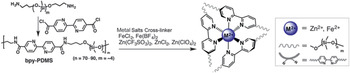
Bao et al. recently reported a new self-healing dielectric elastomer achieved by the incorporation of metal−ligand coordination as cross-linking sites in nonpolar PDMS to realize an intrinsically stretchable TFT with hysteresis-free transfer characteristics. Reference Rao, Chortos, Pfattner, Lissel, Chiu, Feig, Xu, Kurosawa, Gu, Wang, He, Chung and Bao11 The design strategy is demonstrated in Figure 1 . Bipyridine moieties were first embedded into a long PDMS chain that was subsequently cross-linked via metal–ligand coordination between the bipyridine moieties and transition-metal ions, Zn2+ and Fe2+. The advantages of this design include: (1) an increase in dielectric constant by the introduction of metal–ligand coordination bonds; (2) stabilization of the complex cross-linked structure that could potentially provide energy dissipation sites in the bulk material due to the dynamic coordinating ability of the counteranions; and (3) reduction in ion mobility and ionic effects caused by the incorporation of ions in the nonpolar PDMS matrix. As a result, fully stretchable transistors utilizing FeCl2-PDMS as stretchable dielectrics exhibited ideal hysteresis-free transfer characteristics, while the gate leakage current remained low even after 1000 cycles of tensile deformation at 100% strain. Reference Rao, Chortos, Pfattner, Lissel, Chiu, Feig, Xu, Kurosawa, Gu, Wang, He, Chung and Bao11
The synthetic route of poly(dimethylsiloxane) (PDMS) cross-linked through coordination of metal ions to bipyridine (bpy) moieties. Reprinted with permission from Reference Reference Rao, Chortos, Pfattner, Lissel, Chiu, Feig, Xu, Kurosawa, Gu, Wang, He, Chung and Bao11. © 2016 American Chemical Society.

Wrinkled metal oxide
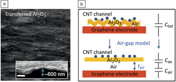
Typical inorganic gate oxides are brittle and prone to defect formation upon deformation, but possess outstanding electrical benefits in TFT dielectric applications compared to dielectric elastomers, which often show higher leakage currents and lower dielectric constants despite their excellent stretchability and good processability. Using a transfer method, the Lee group proposed a new approach for preparing a wrinkled Al2O3 gate dielectric layer, in which out-of-plane motion can accommodate strains applied within the plane ( Figure 2a). Reference Chae, Yu, Bae, Duong, Perello, Jeong, Ta, Ly, Vu, Yun, Duan and Lee8 The wrinkled Al2O3 layer contained effective built-in air gaps that result in a small gate leakage current of 10–13 A. Although the specific gate capacitance of the wrinkled Al2O3 was measured to be 1.49 nF cm–2 at 100 kHz, which is 80× lower than that of planar Al2O3 (Figure 2b), the fabricated devices using SWNTs as the channel material and wrinkled Al2O3 as the stretchable dielectric exhibit no appreciable decrease in performance. This effect is attributed to a strong electric field localized at the valleys of the wrinkles, which allows strict control over the carriers in the SWNT channel giving rise to enhanced device performance. The wrinkled dielectric layer allows the transistors to retain performance under strains as high as 20% without appreciable increase in leakage current, observable physical degradation, or performance loss after stretching and releasing the devices over 1000×.
(a) Scanning electron microscope image of the wrinkled Al2O3 layer. The inset shows a macroscopic wrinkle (scale bar = 1 µm). (b) A schematic of the air-gap model in which the total device capacitance (C tot) is treated as the capacitance of the Al2O3 layer (C ox) and that of an air gap of thickness t air (C air) connected in series. Note: CNT, carbon nanotube. Reprinted with permission from Reference Reference Chae, Yu, Bae, Duong, Perello, Jeong, Ta, Ly, Vu, Yun, Duan and Lee8. © 2013 Macmillan Publishers Ltd.

Elastomeric semiconducting materials and assembly of intrinsically stretchable TFTs
Two-dimensional materials
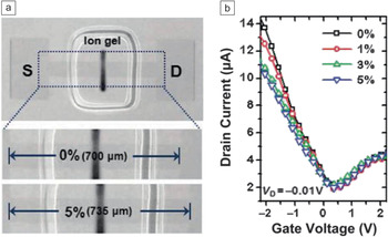
The Ahn and Cho group has described a low-temperature transferring/printing route to fabricate an all-graphene field-effect transistor array on a stretchable rubber substrate. Reference Lee, Kim, Jang, Yoon, Lee, Hong, Rogers, Cho and Ahn9 The source–drain electrodes and semiconducting channels of the all-graphene-based transistors were monolithically patterned from graphene films that were synthesized on Cu foils using chemical vapor deposition (CVD). The ion gel and PSS:PEDOT were printed over the channel to complete the intrinsically stretchable TFT as the dielectric layer and the gate electrode, respectively. The resulting TFT showed hole and electron mobilities of 1188 ± 136 and 422 ± 52 cm2 (V–1 s–1), respectively, and the electrical properties were invariant after 1000 or more cycles at 5% strain ( Figure 3 ). The devices were able to retain their performance despite repeated deformation, mainly because of the extremely large Young’s modulus of graphene or the relaxation of ripples created during the transfer of graphene films to the rubber substrates. However, the characteristic of zero-bandgap semiconductor for graphene causes the TFT to exhibit a low ON/OFF current ratio (<100).
(a) Optical microscope images of graphene-based thin-film field-effect transistors (TFTs) under substrate stretching up to 5% along the longitudinal direction of the channel. (b) Typical transfer characteristics of graphene-based TFTs on poly(dimethylsiloxane) under various strains. Reprinted with permission from Reference Reference Lee, Kim, Jang, Yoon, Lee, Hong, Rogers, Cho and Ahn9. © 2011 American Chemical Society.

Degradation of the device characteristics was also observed at applied strains larger than 5%, possibly due to microcracks initiated at grain boundaries or other defects in the graphene films. The Li and Takenobu groups replaced graphene with two-dimensional (2D) molybdenum disulfide as the channel material to construct stretchable TFTs. Reference Pu, Zhang, Wada, Wang, Li, Iwasa and Takenobu10 Using an ion gel as the stretchable dielectric layer, the TFT on the PDMS substrate displayed an ON/OFF ratio of ∼104, mobility in the range of 0.4–1.4 cm2 V–1 s–1, and small variation in electrical characteristics during stretching up to 4% strain.
One-dimensional nanotube or nanowire networks
A network of semiconducting single-walled carbon nanotubes (semi-SWNTs) is an attractive option for the channel material of stretchable TFTs, due to the mechanical resilience of the nanotubes, the capability to accommodate large strain via nanotube−nanotube sliding and buckling, and the extraordinary charge-transport characteristics of the nanotubes. Reference Xu, Wu, Safron, Roy, Jacobberger, Bindl, Seo, Chang, Ma and Arnold16 The Lee group reported a stretchable TFT combining a semi-SWNT network channel with stretchable graphene/SWNT electrodes and a wrinkled Al2O3 dielectric layer. Reference Chae, Yu, Bae, Duong, Perello, Jeong, Ta, Ly, Vu, Yun, Duan and Lee8 The semi-SWNT network was prepared using atmospheric pressure chemical vapor deposition, transferred onto the patterned graphene electrodes and wrinkled Al2O3 dielectric layer, and patterned using photolithography and O2 plasma etching. The semi-SWNT network not only worked as the channel material, but also prevented the graphene electrodes from being damaged during stretching. The resulting devices exhibited an excellent ON/OFF ratio of ∼105, a high mobility of ∼40 cm2 V–1s–1, and a low operating voltage of less than 1 V. Moreover, the devices that were stretched along the channel length direction up to 16% strain and along the width direction up to 20% strain showed only mild fluctuation in the ON/OFF ratio, without major variation in device performance. In a fatigue test of 10% strain for 1000 stretching and releasing cycles, the ON/OFF ratio, transconductance, and mobility of the devices also fluctuated mildly with no major deterioration. However, the stretchable TFT could not withstand strains larger than 20% in either direction.
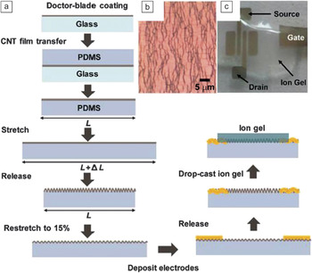
Also utilizing a semi-SWNT as the channel material, the Arnold group substantially modified the TFT design in order to increase the stretchability of the device through (1) buckling of the semi-SWNT thin-film networks in the active channel and (2) integrating the buckled channel with an ion gel as the stretchable dielectric layer and a buckled thermally evaporated Au metal film as the stretchable electrode ( Figure 4 ). Reference Xu, Wu, Safron, Roy, Jacobberger, Bindl, Seo, Chang, Ma and Arnold16 The semi-SWNTs were isolated from as-grown CNTs produced via cobalt molybdenum catalysis of carbon monoxide disproportionation, using poly(9,9-dioctylfluorene) as a selective agent in toluene. The enriched and polymer-wrapped semi-SWNTs were then solution-cast onto glass substrates to form network thin films, followed by transferring onto strained PDMS substrates to form the stretchable channel layer. The resulting TFT performed as a typical p-type channel device with an ON/OFF current ratio reaching 4 × 10⁴ and mobility of 10.6 cm2 V–1 s–1. The devices exhibited fairly stable operation with invariant mobility and an ON/OFF current ratio up to 50.8% strain and did not show significant reduction in performance up to an applied strain of 57.2%.
(a) Schematic showing transfer and buckling of a semiconducting carbon nanotube (semi-SWNT) film on poly(dimethylsiloxane) (PDMS), followed by fabrication of stretchable SWNT-based thin-film field-effect transistors (TFTs). (b) Optical image of electrodes after buckling. (c) Optical micrograph of a SWNT-based TFT. Reprinted with permission from Reference Reference Xu, Wu, Safron, Roy, Jacobberger, Bindl, Seo, Chang, Ma and Arnold16. © 2014 American Chemical Society. Note: CNT, carbon nanotube.

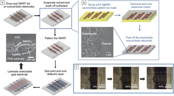
In order to simplify the fabrication process and reduce the production cost of stretchable TFTs, the Pei group developed an all solution-based process to fabricate arrays of fully stretchable semi-SWNTs-based TFTs ( Figure 5 ). Reference Liang, Li, Chen, Hajagos, Ren, Chou, Hu and Pei2,Reference Liang, Tong and Pei13 The stretchable TFT employed a silver nanowire-poly(urethane acrylate) (AgNW-PUA) composite as stretchable electrodes and a PU-co-PEG elastomeric dielectric. The active channel material was printed by drop-casting a formulated semi-SWNT ink that was prepared by mixing a fluorosurfactant and propylene glycol with a 99+% semi-SWNT solution at an optimized ratio.
(a–b) Schematic illustration of the fabrication steps for a stretchable semiconducting carbon nanotube (semi-SWNT)-based thin-film field-effect transistor on a poly(urethane acrylate) (PUA) elastomeric substrate, with spray-printed silver nanowire (AgNW) electrodes. The scanning electron microscope (SEM) image in (a) shows the AgNW-PUA composite source/drain electrodes covered with a semi-SWNT layer (100-mm channel length) and an elastomeric dielectric copolymer (EDC) layer. Inset in (b) is a cross-sectional SEM image showing the SWNTs embedded into and wrapped by the dielectric layer. (c) Photographs of a device at specified strains applied along the channel length direction. Reference Liang, Li, Chen, Hajagos, Ren, Chou, Hu and Pei2

For a total of 36 stretchable TFT devices fabricated with a yield of 85.7%, the average ON/OFF current ratio, ON-current to channel width ratio (I ON/W), transconductance to channel width ratio (g m/W), and mobility measured at V D = –2.0 V were 7200 ± 1200, 30.0 ± 8.93 mA mm–1, 11.2 ± 3.40 mS mm–1, and 27.0 ± 7.44 cm2 V–1 s–1, respectively. The resulting device could be stretched up to 50% along either the channel length or channel width direction without significant decrease in performance. Moreover, the device only showed a mild decrease in mobility after 500 cycles of continuous stretch–relaxation cycles between 0 and 20% strain along the channel-length or channel-width direction. This stability in device performance under large strain and repeated stretch–relaxation deformation resulted from the unique structure, where the elastomeric dielectric layer infiltrates into the semi-SWNT network and wraps around the nanotubes.
Organic channel materials
Even though inorganic semiconductors show better electrical performance than organic semiconductors, other material characteristics, such as mechanical properties, materials availability and compatibility with high-throughput processing, and all-solution processability, allow many organic semiconductors to be an excellent alternative for stretchable electronics. Reference Chortos, Lim, To, Vosgueritchian, Dusseault, Kim, Hwang and Bao7 The O’Connor group conducted research that suggests that a rigid, three-dimensional packing structure of common polymeric semiconductors results in fracture at low strain, while a 2D packing structure of the organic conductor P3HT allows deformation greater than 150% strain. Reference O’Connor, Chan, Chan, Conrad, Richter, Kline, Heeney, McCulloch, Soles and DeLongchamp20
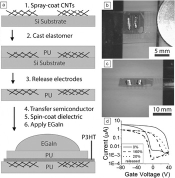
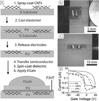
In addition, the Bao group fabricated a top gate architecture of stretchable organic-based TFTs as displayed in Figure 6 . Reference Chortos, Lim, To, Vosgueritchian, Dusseault, Kim, Hwang and Bao7 Patterned CNT-PU elastomer composite electrodes were used as stretchable source and drain electrodes. P3HT films were formed on PU electrodes as the active channel layer, and a 4-μm-thick PU dielectric layer was spin-coated on top, followed by applying eutectic gallium indium, a liquid metal, as the gate electrode to complete the device construction. The average values of device mobility and ON/OFF ratio in the unstretched state are 3.4 × 10⁻² ± 1.63 × 10⁻² cm2 V–1 s–1 and 591 ± 461, respectively. Strikingly, the devices still exhibited transistor characteristics when stretched up to strains as large as ∼265%.
(a) Schematic of the fabrication process for a stretchable organic-based thin-film field-effect transistor with a poly(3-hexylthiophene) (P3HT) channel layer, polyurethane (PU) dielectric, carbon nanotube (CNT) source and drain electrodes, and a eutectic gallium indium (EGaIn) gate electrode. Microscope image of a device with (b) zero and (c) 150% applied strain. (d) Transfer curves for a device stretched to 160% and released to 20%. The source–drain bias was −20 V and the channel width-length ratio (W/L) is 40. Reprinted with permission from Reference Reference Chortos, Lim, To, Vosgueritchian, Dusseault, Kim, Hwang and Bao7. © 2014 Wiley.
The Jeong group further constructed a stretchable polymer-based TFT by employing stretchable Au nanosheet electrodes with an ion gel for the gate dielectric, Reference Shin, Song, Lim, Lim, Park and Jeong12 and electrospun P3HT nanofibers for the active channel material. Au was selected because of its low energy barrier for charge injection into the P3HT fiber network. The measured hole mobility of the device was 23 cm2 V–1 s–1 in the saturation regime at V D = −1 V. Upon deformation, the mobility maintained the same value up to 40% strain and slightly decreased to 16 cm2 V–1 s–1 at 70% strain. Moreover, the device exhibited outstanding mechanical durability with a stable ON/OFF current ratio and an unchanged threshold voltage (V th) during a fatigue test of 1500 cycles. All these results indicate excellent mechanical compliance of stretchable polymer-based TFTs.
Conclusions and outlook
The emergence of devices that combine elasticity with electronic or optoelectronic properties are still facing significant materials challenges. Collectively, advances in materials and engineering, as summarized in this article, provide three promising strategies to design elastomeric materials for intrinsically stretchable TFTs. First, conventional rigid or nonstretchable materials could be fabricated into new structures such as buckling structures and networks of metallic nanowires to provide stretchability. For instance, while bulk silver is rigid without elasticity, the new silver structure—one-dimensional AgNWs—can form thin-film networks that can retain the high conductivity of silver while accommodating large strain. Second, nanoscale functional materials could be embedded into elastomeric matrices to fabricate stretchable nanocomposites. Achieving highly uniform nanomaterials dispersion and the compatibility of the material interface of the nanomaterial and the matrix material are the major challenges to improve the synergistic effect of the fillers and matrix elastomers. Third, novel functional elastomers could be designed and synthesized to produce elastic-yet-high-performance molecular materials, as highlighted in a recent review by Lipomi. Reference Savagatrup, Printz, O’Connor, Zaretski and Lipomi21 Investigative studies for the better understanding of the relationships between molecular structure and physical properties of the materials will be beneficial for future developments in this field.
Beyond material design, further development in processing/fabrication techniques to assemble the different stretchable components congruently to construct intrinsically stretchable TFT and arrays in cost-effective and reliable methods is also needed. Conventional deposition methods used in the electronic industry that require high-temperature and high-vacuum processing conditions are often undesirable for the deposition of elastomeric materials. With this in mind, developing solution-based printing technologies to assemble intrinsically stretchable TFTs is a promising research direction to reduce fabrication costs and to seek more suitable methods to fabricate devices with these new materials.
Acknowledgments
This research was supported by the Air Force Office of Scientific Research (Grant No. FA9550-12-1-0074), the National Science Foundation (Grant No. 1638163), and the Ministry of Science and Technology of China (Grant No. 0102014DFA52030).

Jiajie Liang is a full professor in the School of Materials Science and Engineering at Nankai University, China. He leads the Stretchable and Printed Electronics Group, which studies and fabricates new functional materials to enable innovative applications on various kinds of stretchable electronics via novel, low-cost, scalable microfabrication and printable methods. He obtained his PhD degree in polymer chemistry and physics from Nankai University in 2011. He worked as a postdoctoral researcher at the University of California, Los Angeles, from 2011 to 2016. Liang can be reached by email at liang0909@nankai.edu.cn.

Kwing Tong is currently completing his PhD degree in the Department of Materials Science and Engineering at the University of California, Los Angeles. He received his bachelor’s degree in biomedical engineering from the University of California, Irvine, in 2009. His current research focuses on synthesizing multifunctional polymers and investigating the structure–property relationships of nanomaterial–polymer composites to develop transparent conductors via cost-effective scalable fabrication methods for flexible and stretchable electronics. Tong can be reached by email at kwing.tong@gmail.com.

Huibin Sun is a postdoctoral fellow at the University of California, Los Angeles, sponsored by the China Scholarship Council. He obtained his PhD degree in information materials from Nanjing University of Posts and Telecommunications, China. He then joined the Institute of Advanced Materials at Nanjing Tech University, where he studied the development of stimuli-responsive organic optoelectronic materials and the application of information storage, display, and biosensors. His current research focuses on flexible electronic systems. Sun can be reached by email at sunhuibin003@gmail.com.

Qibing Pei is a professor of materials science and engineering at the University of California, Los Angeles. He has developed a number of electronic and electroactive polymers for applications in electro-optic and electromechanical devices, including light-emitting diodes, polymer light-emitting electrochemical cells, electroactive polymer artificial muscles, and biologically inspired robots. His research interests include a wide range of soft materials and span material synthesis and processing to design of functional devices. He applies polymer synthesis, solution-based processing, and nanofabrication in the discovery of new functional polymers and composites. Pei can be reached by phone at 310-825-4217 or by email at qpei@seas.ucla.edu.