Introduction
Radiation in nuclear applications adversely influences the microstructure of the fuel, cladding, and other component materials. Depending on the radiation fluence, flux, temperature, and other environmental conditions, such influence on grain size, shape, texture, and dislocation density may inflict anisotropic dimensional change, hardening, and even amorphization.[Reference Zinkle and Was1, Reference Yan, Wang, Wang, Wang and Bai2]. This is manifested with the loss of ductility and plastic instability that is known to degrade the structural performance of these materials.[Reference Was3] Zirconium and its alloys have been historically popular as cladding materials because of their low-thermal neutron capture cross-section, high temperature, corrosion resistance, and satisfactory mechanical properties. Post-irradiation, mechanical behavior of zirconium and Zr alloys is characterized by an increase of yield strength and hardness,[Reference Dayal, Bhattacharyya, Mook, Fu, Wang, Carr, Anderoglu, Mara, Misra, Harrison and Edwards4, Reference Sarkar, Kumar, Mukherjee, Sharma, Dutta, Pujari, Agarwal, Gupta, Singh and Chakravartty5] which comes at the cost of reduced ductility and fracture toughness.[Reference Zinkle and Was1]
This study is motivated by the application potentials of nanocrystalline materials, which are hypothesized to exhibit better resistance to irradiation by reducing irradiation-induced dislocation and cavity density.[Reference Liu, Ji, Tan, Zang, He, Yun, Zhang and Yang6] It is postulated that grain boundaries in nanocrystalline systems are effective sinks for radiation-induced defects. Since the volume fraction of grain boundary increases exponentially at <25 nm grain size, nanocrystalline materials may exhibit enhanced radiation tolerance.[Reference Beyerlein, Caro, Demkowicz, Mara, Misra and Uberuaga7] There is also indication that radiation tolerance could be grain size dependent and strongly influenced by temperature.[Reference Cheng, Xu, Wang, Misra and Zhu8] At these grain sizes, nanocrystalline metals also show very high strength and low ductility.[Reference Argon and Yip9] We hypothesize that radiation-induced defects are actually beneficial at this length scale, because of the very high strength due to defect confinement and increases in mobile defect density (due to irradiation) enhancing ductility. We therefore design a set of experiments where irradiation is performed on specimens with initial grain sizes around 10 nm and then measure their mechanical properties inside a transmission electron microscope (TEM), so that the irradiation-induced micro-structural changes could be connected to the deformation behavior. In particular, we employ self-ion irradiation, which is suggested to be a surrogate of neutron irradiation with distinct advantages such as: (a) lower time and cost since damage rates (~10−2 dpa/s) are higher compared with the typical ~10−7 dpa/s for nuclear reactors, (b) little or no residual radioactivity, and (c) precise control of irradiation conditions.[Reference Idrees, Yao, Kirk and Daymond10] The majority of ion irradiation studies in Zr to date have been focused on coarse grain, bulk, and alloys.[Reference Hengstler-Eger, Baldo, Beck, Dorner, Ertl, Hoffmann, Hugenschmidt, Kirk, Petry, Pikart and Rempel11, Reference Yamada and Kameyama12] The effect of ion irradiation for nanocrystalline zirconium is therefore yet to be completely understood.
Experimental setup
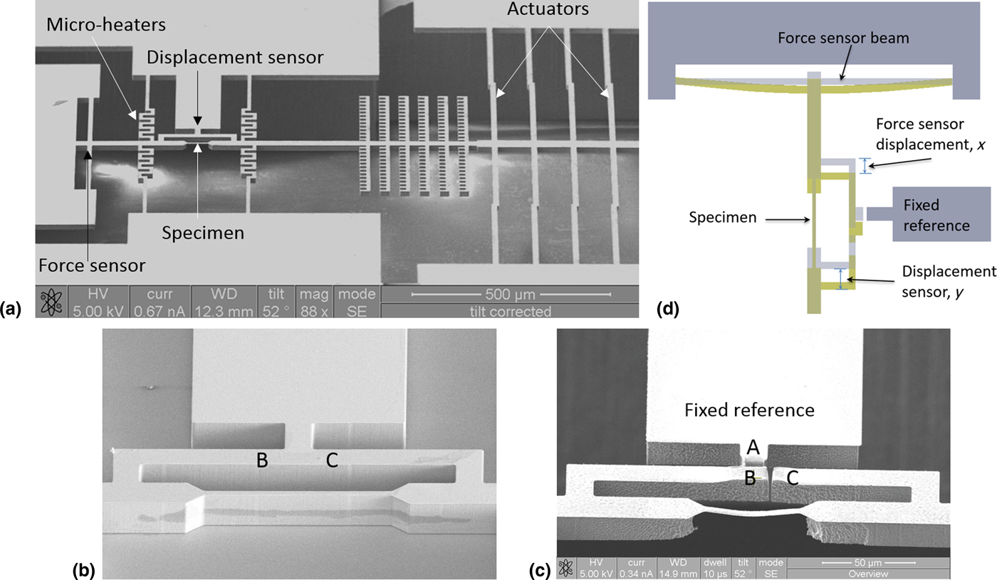
To study our hypothesis that radiation induces beneficial features to nanocrystalline metals, we developed a set of experiments where uniaxial tensile tests are performed on self-ion irradiated specimens. The process starts with design and fabrication of a micro-electro-mechanical (MEMS) device. As shown in Fig. 1a, the devices integrates electro-thermal actuators, mechanical displacement sensors with the specimen. Thin zirconium films of 99.99% purity were sputter deposited on a silicon-on insulator wafer with 20 µm-thick device layer. The device design was then patterned on the wafer using photolithography and subsequent deep reactive ion etching on both front and backsides using techniques detailed elsewhere.[Reference Kumar and Haque13] At this stage, the specimen is not freestanding and the two reference points (marked as B and C) on its two ends are connected. We then perform ion irradiation on the device, which has been a popular surrogate for neutron irradiation.
(a) Micro-machined electromechanical device for mechanical testing of thin films (b) zoomed-in view of the specimen gauge section before ion irradiation; (c) the same location after ion irradiation and subsequent substrate etching; (d) schematic showing displacement and force measurement.

After the ion irradiation, the silicon substrate underneath the specimen gauge length is selectively removed using isotropic reactive ion etching. This step releases the specimen from the substrate (Fig. 1c). The freestanding specimen remains suspended and essentially spring-loaded by the micro-machined silicon beams. We then use a focused ion beam to cut a narrow slit to separate the two ends of the specimen frame (marked as B and C). Similarly, we separate the two points (marked as A and B), so that the displacements of the left and right ends of the specimens can be measured by comparing the motion of the points B and C, respectively, from the immobile location A. In a typical experiment, the 3 mm × 5 mm footprint device is mounted on a commercially available TEM holder for in situ electrical biasing. The actuation imposes a displacement to the silicon structures, which is transmitted through the specimen. The displacement on the left side of the specimen is taken by the force sensing. This displacement (x, in Fig. 1b) gives the force on the specimen when multiplied by the spring constant of the silicon beams. The displacement at the right side of the specimen (y) is the rigid body motion of the actuators. The difference between these two displacements (y–x) is the specimen elongation. Figure 1d shows the displacement measurement schemes. These displacements are measured inside the TEM, which makes the measurements slow, but robust and accurate. We achieve about 50 nm displacement resolution in our in situ TEM experiments, which gives at least 0.1% strain resolution for a nominally 50 µm-long specimen.
Experimental results and discussion
Individual dies containing multiple partially processed micro-fabricated samples were ion irradiated with an 800 keV Zr+ beam using the 6 MV HVE Tandem accelerator at Sandia's Ion Beam Laboratory. The ion energy was chosen based on a stopping and range of ions in matter (SRIM) simulations[Reference Ziegler, Ziegler and Biersack14] to have a relatively uniform damage profile. The six doses achieved were: 3 × 10¹⁰, 3 × 10¹¹, 3 × 10¹², 3 × 10¹³, 3 × 10¹⁴, and 3.26 × 10¹⁴ ions/cm2. Irradiation damage in Zr/Si specimen by 800 keV Zr ions was calculated using SRIM-2013 with full damage cascades and the displacement energy of 40 eV, typical for metals.
Damage level in term of displacement per atom can be calculated as:
 $${\rm dpa} = \displaystyle{{\Oslash \times {10}^8 \times {\rm Damage\; rate}} \over N}$$
where ø is the fluence in ions/cm2. The damage rate expressed in vacancies/ion/A° is obtained from SRIM. We used an average damage rate of 1.8 vacancies/ion/A° was used in the calculation, and N is the atomic number density 4.28 × 10²² atoms/cm3. It is predicted using SRIM that this ion irradiation conditions will result in damage levels in the 100 nm-thick Zr film of 1.26−04, 1.26−03, 1.26−02, 1.26−01, 1.26, and 1.36 dpa (peak value through the Zr thickness), respectively. After irradiation, the silicon substrate beneath the specimen is etched away using reaction ions of SF6 and O2. At least three specimens of each irradiation dosage were first investigated for micro-structural changes and then tested for uniaxial stress–strain behavior. All the experiments were performed at room temperature.
Irradiation effects on microstructure
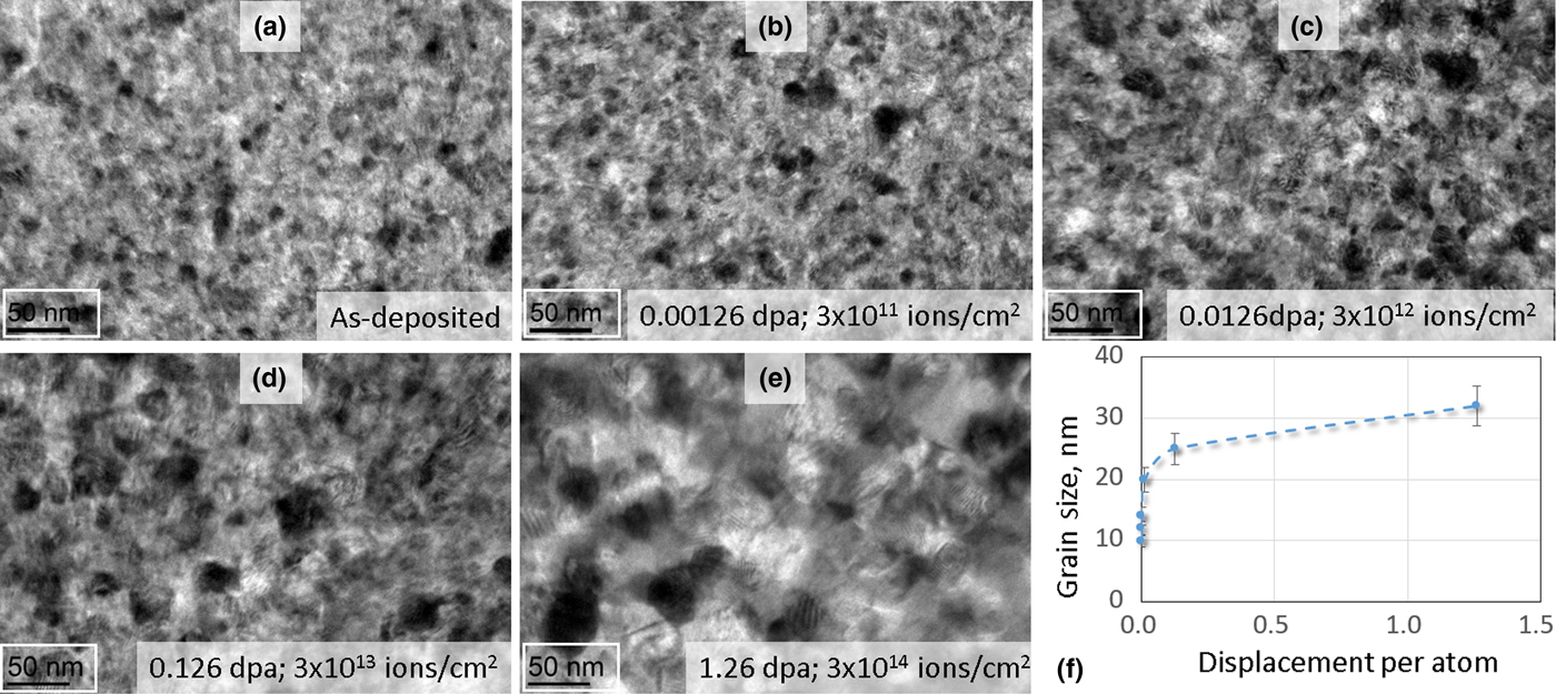
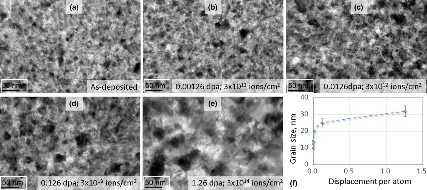
Figure 2 shows bright-field TEM images of the specimens as function of the radiation dosage and associated damage level. We measured the average grain size of the specimens from the TEM images using the intercept technique. The as-deposited specimens had average grain size of 8–10 nm. While the average grain size is representative of the ensemble, the specimens had few larger grains. The effect of irradiation was grain growth, which was prominent for all doses. While irradiation-induced grain growth is consistent across the literature,Reference Cheng, Xu, Wang, Misra and Zhu8, Reference Bufford, Abdeljawad, Foiles and Hattar15, Reference Motta, Kaoumi and Birtcher16 the underlying mechanisms may not be the same. Ion irradiation-induced grain growth exhibits three regimes: (i) a purely thermal regime, (ii) a thermally assisted regime where thermal motion and irradiation effects combine to increase the rate of grain growth, and (iii) a low-temperature regime, where ballistic (direct collisional impacts) effects at the grain boundaries dominate the grain growth process.[Reference Motta, Kaoumi and Birtcher16] From Fig. 2f, we observe that the grain growth kinetics is very pronounced for the smaller grain sizes where the displacement damage is very low (<0.1 dpa). As the dpa value increases, the grain growth rate tapers off. This suggests that the growth rate is more dependent on the initial grain size than the irradiation dosage. Defect-driven models are therefore more appropriate for this study,[Reference Zhang, Edmondson, Varga, Moll, Namavar, Lan and Weber17] where the high concentration of irradiation-induced defects caused by collision cascades would pronounce atomic diffusion and mobility at the grain boundaries. This is enhanced below the 20 nm scale, causing grain growth to the very sensitive to even smallest dpa levels. We used an atomic force microscope to measure the surface roughness of the specimens. The as-deposited specimens showed rms roughness of about 2.5 nm. We did not observe any appreciable change in this value for the various irradiation dosage.
(a–e) TEM images of the specimens after various levels of irradiation damage, (f) increase in measured grain size from the 10 nm as-deposited value as function of irradiation damage.
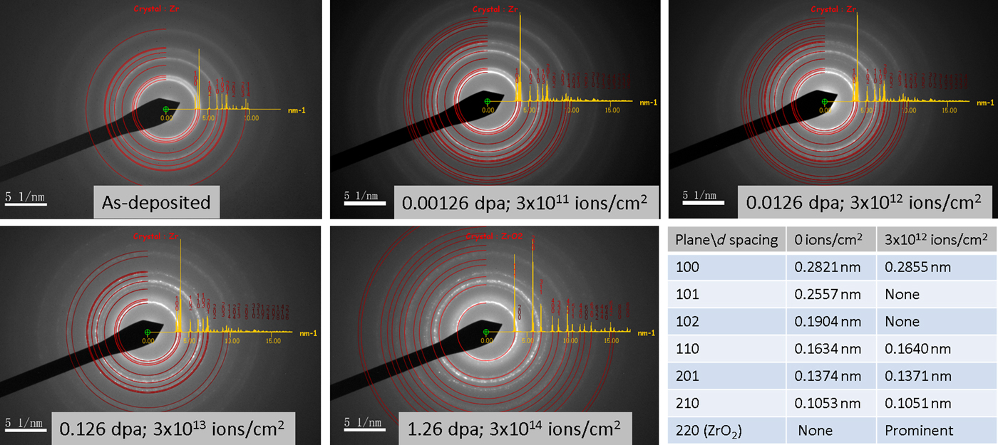
In addition to grain growth, irradiation leads to crystallographic orientation through texture development as shown in Fig. 3. The selected area electron diffraction patterns becomes discontinuous or spotty (reflecting grain growth) and the rings associated with various crystallographic planes appear or disappear, suggesting changes in composition or texture. For example, the {101} and {102} planes become weak or invisible, while the {100} plane becomes prominent. From the diffraction patterns, we measured the inter-atomic spacing of these planes, which shows strain fields generated, resembling anisotropic diffusion-driven growth in absence of any external mechanical loading. Figure 3 also shows oxidation of zirconium (at about 0.126 and 1.26 dpa), where an additional ring representing the {220} plane in ZrO2 was clearly visible. This can be explained by the formation of an oxide originating from trace oxygen in the ion beam line during ion irradiation. Such oxide has been shown to impede defect mobility during annealing in nanocrystalline Ni.[Reference Muntifering, Dingreville, Hattar and Qu18]
Selected area electron diffraction patterns of the specimens at various irradiation dosage.

Irradiation effects on mechanical properties
Uniaxial tensile tests performed on the irradiated specimens showed strong influence on both elastic and plastic properties. The as-deposited specimens showed no visible plastic deformation mechanisms and the stress–strain diagram was linear elastic up to failure. This is typical for nanocrystalline metals with grain sizes smaller than the inverse Hall-Petch or the cross-over size.[Reference Arzt19] Here the grain is too small to accommodate any significant dislocation activity, as such the grains are typically referred to as dislocation starved. For higher doses, vacancy clusters are thought to agglomerate into dislocation loops. Irradiation in nanocrystals therefore add plastic deformation mechanisms.
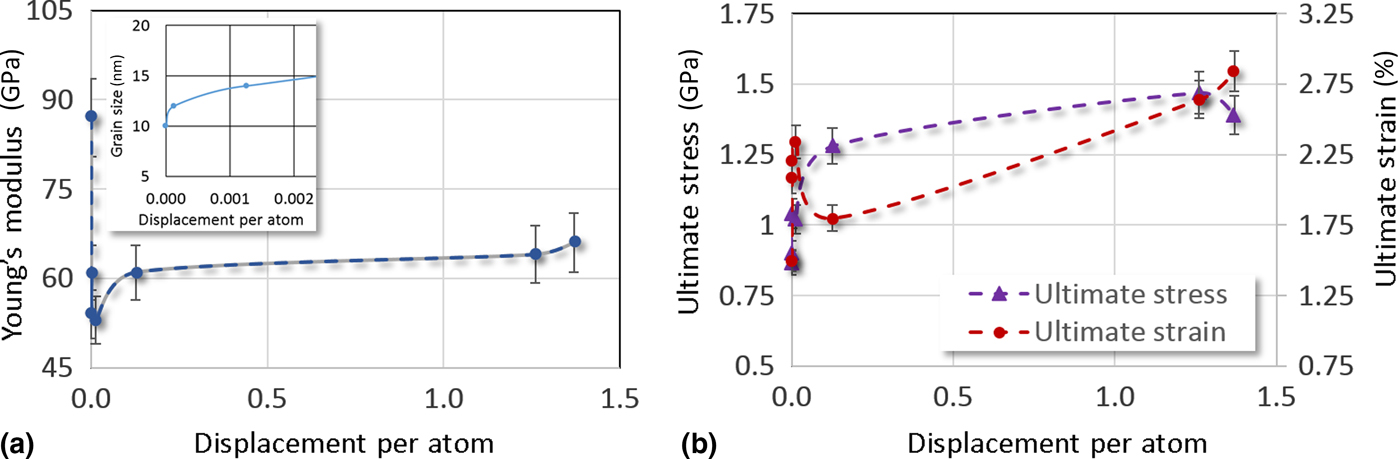
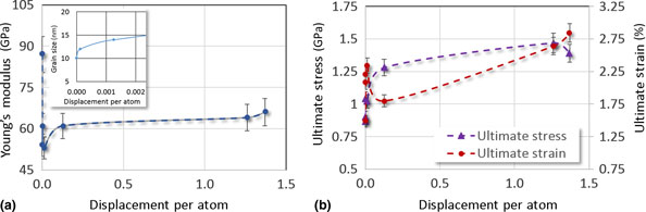
Experimental results on elastic and plastic properties of self-ion irradiated zirconium thin films are shown in Fig. 4. Since the as-deposited grain size is below 10 nm, the volume fractions of grain boundary and triple junction are significantly larger than bulk and also strong functions of the grain size. The abundance of these effective sinks for radiation-induced defect sinks imply increased atomic disorder. Therefore, below 10 nm grain size, Young's modulus a very sensitive function of radiation damage, even for the smallest dpa values. However, this pronounced influence is quickly, radiation also results in grain size increase as shown by the inset of Fig. 4a. The increase of grain size implies that the volume fraction of grain boundaries is not very high any more for higher damage levels. Figure 4a suggests that the influence role of irradiation on the moduli is negligible for grain sizes greater than about 20 nm. Above this grain size, the fraction of grain boundary atoms falls below 10%,[Reference Hahn and Meyers20] which nullifies the sensitivity of the non-equilibrium grain boundary structure. Above 20 nm grain size (0.126 dpa), we observe the familiar increasing trend. Interestingly, this is also the grain size where we start observing plastic deformation in the specimens. As shown in Fig. 4b, both ultimate stress and strain increase in samples exposed to higher doses. Therefore, the role of irradiation damage is twofold, (a) increase the grain size and (b) supply additional defects in the previously dislocation-starved grains with mechanisms for plasticity. However, the maximum grain size in this study is too small compared with bulk to accommodate large densities of dislocations, so that the ultimate strain is still below 5%.
Effect of self-ion irradiation on (a) Young's modulus (inset shows the grain size as function of damage that correlates grain size with Young's modulus) and (b) strain hardening of nanocrystalline (as-deposited grain size ~10 nm) zirconium thin films.

According to the findings of this study, the effect of self-ion irradiation in nanocrystalline zirconium (and potentially metals, in general) manifests in the micro-structural change in grain size and local texture, which in turn dominates the mechanical properties. This is essentially similar in nature for unirradiated grain sizes, suggesting that the defect density is the key player in the mechanics of nanocrystalline metals. For grain sizes below a cross-over value (d c), the grain interior is dislocation starved and large fraction of atoms resides in the grain boundaries, away from the equilibrium positions. The lack of statistically significant dislocation density results in the mostly elastic behavior,[Reference Wang, Tomar and Haque21] as seen in our stress–strain diagrams. On the other side, grain sizes greater that d c can accommodate the left-over vacancies (after the vacancy-interstitial recombination) that evolve as dislocation loops. Therefore, the dislocation density increases as a direct effect of irradiation-induced grain growth. This is evident from the plastic behavior of the samples. From our mechanical properties measurement, we observe the incipience of plastic deformation at grain size around 20 nm, which is very close to the cross-over grain size cited in the literature. Grain growth above d c opens up the dislocation-based deformation window since the grains can accommodate adequate density of dislocations to permit classical plasticity mechanisms. These dislocations are either nucleated from the vacancy clusters that agglomerated or from the grain boundaries experience less repulsive force for dislocation nucleation. If the grain size is in the nanocrystalline range (100 nm), it is too small to activate large-scale activity in slip systems for dislocation climb and glide that is necessary for plastic instability (commonly observed in bulk scale). As a result of this balance between grain size and dislocation density, we observe strain hardening instead of plastic collapse. It is important to note that all these mechanisms evolve from the atomic collision events at the grain boundaries, so the abovementioned elasticity and plasticity effects slow down rapidly as the grain size increases beyond the cross-over value.
Conclusions
The effect of ion irradiation on the microstructure and mechanical properties nanocrystalline zirconium was studied in situ inside a TEM. The specimens with average grain size of about 10 nm were irradiated at room temperature with an 800 keV Zr+ beam using a 6-MV HVE Tandem accelerator to achieve displacement per atom ranging from 2.1 × 10⁻⁴ to 2.28. The experimental measurements and observations lead to the following conclusions:
(1) The primary effect of self-ion irradiation is to inject vacancies and their clusters in the grain boundaries of the nanocrystalline metal. The abundance of grain boundaries at the nanoscale strongly influence the evolution of microstructure (and hence properties).
(2) Below about 15 nm grain size, the Young's modulus is very sensitive to irradiation. However, a direct consequence of irradiation is grain growth, which leads to recovery of the Young's modulus at higher damage levels.
(3) Strength and ductility are influenced by irradiation in a different manner than the bulk. Because the specimens are nanocrystalline, they exhibit very high strength but low ductility because of dislocation starvation. At the same time, the high-volume fraction of grain boundaries are infused with the defects from radiation – thereby giving the plastic deformation mechanisms to increase ductility. We therefore observed sustained strain hardening, indicating improved radiation tolerance at the 10–30 nm grain size range.
Acknowledgment
B.W. and M.A.H. acknowledge the support of the US Department of Energy through a NEUP funding (DE-NE0000696). M.A.H. also acknowledges support from the National Science Foundation (DMR 1609060) to carry out the MEMS fabrication at the Pennsylvania State University Nanofabrication Facility. The ion irradiation was carried out at the Sandia National Laboratories. The in situ TEM experiments were performed at the Materials Characterization Laboratory at the Pennsylvania State University. The authors would like to thank Daniel Buller for his assistance with the ion irradiation. This work was performed, in part, at the Center for Integrated Nanotechnologies, an Office of Science User Facility operated for the US Department of Energy (DOE) Office of Science. Sandia National Laboratories is a multi-program laboratory managed and operated by Sandia Corporation, a wholly owned subsidiary of Lockheed Martin Corporation, for the US Department of Energy's National Nuclear Security Administration under contract DE-AC04-94AL85000.