I. INTRODUCTION
Radio frequency identification (RFID) is a technology that can be applied almost everywhere. A plethora of RFID applications in primary sectors of the economy include smart cards, smart tickets, retail stores, animals, firefighters, manufacturing, air baggage, passports, drugs, healthcare and pharmaceutical industry, consumer goods, postal services, warehouses, libraries, logistics, energy, and tracking [Reference Polycarpou1, Reference Peng2]. In addition to other benefits, RFID technology can be effectively used in low-cost applications of several resource management systems. RFIDs change work practice and the old paradigm. They expand the role of system integration and mainly change the market of products and services. Productivity and effectiveness improvement, as well as labor reduction, are the main results of work practice transformation [Reference Linquist3]. RFIDs reduce running cost, theft count, and the number of missing or misplaced items. An RFID system contains the reader, which generates the RF broadcasted signal via its antenna. The signal is received by the tag's onboard antenna. A portion of the radio signal is modulated by the chip pre-programmed data and backscattered to the reader. Reader decodes the received signal and passes data on the corresponding aggregation device and the host system. The reader antenna constitutes a critical device that characterizes the read range and the area of coverage.
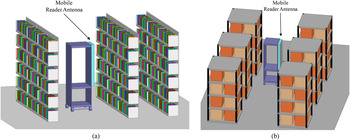
In this paper, two different designs of an ultra-high-frequency (UHF) RFID reader antenna are presented in detail. The first one is a narrowband antenna, suitable for the frequency band of the ETSI standard (865–868 MHz), and the other one is a wideband antenna that operates in both the frequency bands of ETSI and FCC (865–928 MHz) standards. Both antennas are intended to be used for the search of existing, misplaced, or lost tagged items. A library and a warehouse are the two environments of specific interest. A microstrip array of mutually orthogonal elements, which are fed in series by a microstrip line, constitutes (in both designs) the antenna of the reader. The elements of the antenna are excited such as to produce two orthogonal electric-field components. Thus, the antenna creates beams with direction diversity [Reference Sahalos4]. As a result, it is expected to have polarization matching with the tags irrespective of tag orientation. Figure 1 presents two cases of an RFID system in front of shelves loaded with goods. The reader is installed on a trolley along with the antenna. The antenna array is mounted vertically on one or both sides of the trolley and is connected to the corresponding input port of the reader. Four appropriate wheels are attached at the base of the trolley to facilitate its movement.
A mobile UHF RFID reader antenna for searching tagged items in: (a) a library and (b) a warehouse.

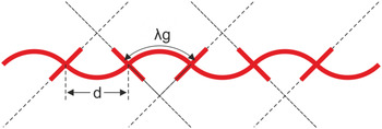
Figure 2 represents a mutually orthogonal dipole array which constitutes the reader antenna. The array follows the characteristics given in [Reference Burnside, Burkholder and Tsai5]. A meander-shaped microstrip line is used for the excitation of the dipoles and, as will be shown later, the meander line achieves the appropriate phase adjustment. Such an array was first designed in the UHF FCC frequency band by Burnside et al. [Reference Burnside, Burkholder and Tsai5]. In the present work, any phase difference for any inter-element distance is achieved and the antenna is designed for wide bandwidth. It is noted that the bandwidth is obtained by increasing the element bandwidth and, at the same time, by suitable derivation of the inter-element distance in conjunction with the other geometrical characteristics of the antenna. Therefore, it is not believed that the whole procedure is a conventional one. Our preliminary efforts to extend the design of [Reference Burnside, Burkholder and Tsai5] were made recently by the authors [Reference Boursianis, Samaras, Polycarpou and Sahalos6, Reference Boursianis, Samaras, Polycarpou and Sahalos7]. In this paper, analytical details are given explaining the design cases of the narrowband (ETSI) and the wideband (ETSI + FCC) antennas. Also, a parametric design study is explained and several field distributions present the areas of coverage. Moreover, specific characteristics of the antenna in the fabrication stage and soldering are given. The above are the facts that differentiate the design procedure of this paper from the presented in [Reference Burnside, Burkholder and Tsai5–Reference Boursianis, Samaras, Polycarpou and Sahalos7]. It is worth noting here that the design and study of near-field antennas are important in the area of wireless power transfer, as well, given the fact that passive RFID tags can be considered as the devices powered at a distance most often [Reference Tak, Park and Nam8].
A meander-shaped microstrip line to excite mutually orthogonal dipoles.

The text is organized as follows: In Section II, an analysis of the meander-shaped line geometry for the element excitation is given. Onwards in Section III, the proposed antenna designs are evaluated in terms of their bandwidth, electric field coverage, and the inter-element distance. A series of simulations was performed using commercial EM software (ANSYS High Frequency Structure Simulator (HFSS) [9], SEMCAD-X [10]) in order to optimize the radiation characteristics of the two antenna designs. The use of two different numerical software packages allows for the validation of results by each one against the other, as well as, for taking advantage of software-specific advantages, such as optimization routines. Also, measurements were conducted on the fabricated wideband antenna prototype and the derived results were compared with simulations. In Section IV, the proposed wideband antenna was placed and simulated in front of a library cabinet in order to evaluate its electric field coverage and examine the items' readability with respect to tag orientation. Our objective is focused on providing adequate coverage of items placed at nearby cabinets (Fig. 1). Finally, in Section V, a summary of the preceding work is outlined and conclusions are stated.
II. MEANDER-SHAPED LINE ANALYSIS
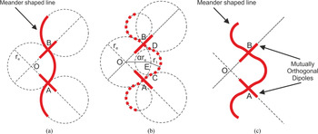
Generally, a meander-shaped line (Fig. 2) is a suitable solution for linear array excitation, whereas a normal line is not able to give the appropriate phase difference. However, it is pointed out that in the meander line of Fig. 2, when the distance between the elements of the array (inter-element distance) is fixed, the phase difference cannot be adjusted, because it is also fixed. For an adjustable phase difference between the elements of the array, the design problem should be tackled with a different procedure. Figure 3(a) represents the initial geometry of a meander-shaped line that interconnects two mutually orthogonal dipoles [Reference Burnside, Burkholder and Tsai5]. The distance between the dipoles at the positions A and B is
 $AB=d={r_e}\sqrt 2 $
, where r
e
is the radius of the circle. The arc length of the meander is
 $\lpar AB\rpar =\pi\, {r_e}/2$
. If we choose a fixed inter-element distance
 $d/\lambda={r_e}\sqrt 2 /\lambda $
, then the corresponding arc length (and the phase difference between the elements) is also fixed and produce a phase difference
 $\Delta \varphi=\pi \lpar \!\pi\, {r_e}/\lambda \rpar $
. If, for example, we want to have the dipoles in phase, then the inter-element distance will be
 $d\, /\, \lambda \, =\, 2\sqrt 2 \, /\, \pi \approx 0.9$
. It is clear that, if the inter-element distance is different than 0.9λ, it is not possible to have the two dipoles in phase. To vary arbitrarily the phase difference between the dipoles, a modification of the meander line that interconnects the dipoles is required. The proposed geometry (modified meander-shaped line length) is given in Fig. 3(b) and the final form of the meander-shaped line is depicted in Fig. 3(c). From Fig. 3(b) we can derive that the distance between the two dipoles remains
 $AB=d={r_e}\sqrt 2 $
, whereas the arc length of the meander (AB) is given by:
(a) The initial geometry of a meander-shaped line with two mutually orthogonal dipoles; (b) the arc (AB) = (ABCD) of the proposed geometry; (c) the final form of the proposed meander-shaped geometry and the position of the two dipoles.

 $$\eqalign{\lpar AB\rpar \, & =\, \lpar ACDB\rpar \, \cr & = \, 2{r_e}\left[{\varphi+\lpar \rpar \left({\sqrt {4+{a^2} - 2\sqrt 2 a} - 1} \right)\left({\varphi+\displaystyle{\pi \over 4}} \right)} \right]}\comma \; $$
where φ is given by
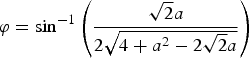 $$\varphi={\sin ^{ - 1}}\left({\displaystyle{{\sqrt 2 a} \over {2\sqrt {4+{a^2} - 2\sqrt 2 a} }}} \right)$$
and α is a constant satisfying the equation:
 $$\lpar \hbox{O}\hbox{E}\rpar \, =\, \; \alpha {r_e}$$
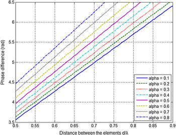
Equations (1) and (2) are given also in [Reference Boursianis, Samaras, Polycarpou and Sahalos7]. However, the final solution that results from the combination of the two equations was not available. Here (see Fig. 4) the distance between the elements versus their phase difference Δφ = 2π/λ(ACDB) for various values of constant α is given.
The phase difference between the elements of the array versus their distance for various values of constant α.

The meander length (ACDB) can be adjusted by using the appropriate value of α. For example, if we set the distance of the dipoles (AB) = 0.75λ and (ABCD) = λ, a modified meander length can be derived with
 $\alpha \cong 0.65$
. In this case, the dipoles are mutually orthogonal having in-phase excitation and the desired inter-element distance. An antenna array with the above characteristics is expected to have a radiated electromagnetic field with polarization and beam diversity. Thus, it is evident that there will be ‘some beam components with polarization matching for each RFID tag’ [Reference Burnside, Burkholder and Tsai5–Reference Boursianis, Samaras, Polycarpou and Sahalos7].
III. ANTENNA ARRAY DESIGNS
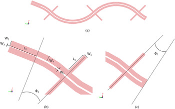
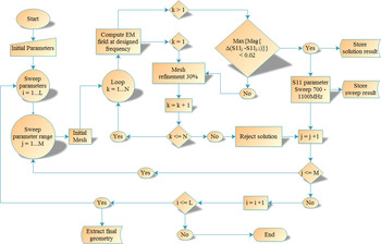
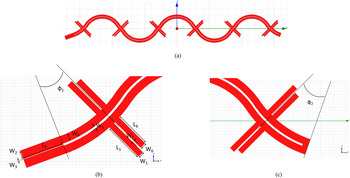
The first objective of this study is to design a narrowband reader antenna in the frequency band of UHF ETSI standard. This case is simple and has similarities with [Reference Burnside, Burkholder and Tsai5]. The antenna array has three dipoles and its size is useful for areas of small height. The dimensions of the antenna are proportional to the ones used in [Reference Burnside, Burkholder and Tsai5] for the frequency band of the UHF FCC standard. It consists of mutually orthogonal printed dipoles that are excited by a meander-shaped feed line (Fig. 5). The feed line is composed of a pair of coplanar strips and has a characteristic impedance of 72 Ω. The dipoles are designed to be resonant at the frequency of 867 MHz and have an input impedance of 72 Ω. The antenna array is positioned between a substrate and a superstrate layer of polystyrene foam with a relative permittivity of 2.5. The dimensions (length × width) of the foam are 900 × 215 mm2, and the layer thickness is 31 mm (for the substrate) and 18 mm (for the superstrate), respectively. The input impedance of the source is 50 Ω and the characteristic impedance of the input quarter-wavelength transformer is 60 Ω. The length of the short end of the antenna is chosen to be in matching conditions at 867 MHz. The final geometry of the stripline, including the orthogonal dipoles and the input transformer, is derived in separate processes using the HFSS commercial software. The finalized geometry of the narrowband antenna consisting of three dipoles has been analyzed and optimized using HFSS and SEMCAD-X. The parameters of the finalized antenna geometry (see Figs 5(b) and 5(c)), which are extracted based on a parametric study, are: L 1 = 63.1 mm, W 1 = 10.4 mm, L 2 = 72.8 mm, W 2 = 15.08 mm, W 3 = 1.04 mm, W 4 = 13.52 mm, W 5 = 4.16 mm, φ 1 = 23.5°, and φ 2 = 17.9°. The procedure followed in the parametric study, along with the required steps involved, is illustrated in the block diagram of Fig. 6. The dipoles are excited in phase at 867 MHz and their inter-element distance is d = 0.9λ.
(a) A three-dipole array with two parallel strip lines (top view – XY-plane); (b) details of the antenna geometry at the input quarter-wavelength transformer; (c) the short end of the antenna geometry.

Block diagram of the parametric study conducted for the final geometry extraction.

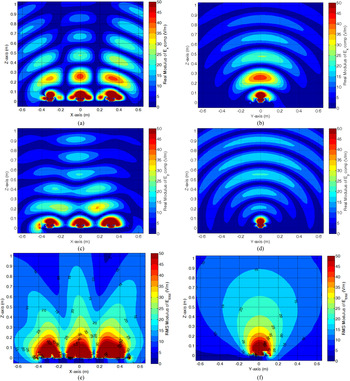
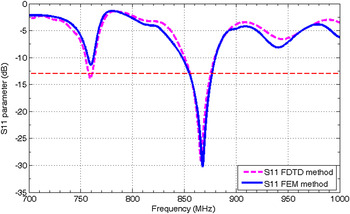
Figure 7 shows the electric field distribution (7(a)–7(d): absolute values of E x and E y electric field components, 7(e)–7(f): root mean square (RMS) values of the E total electric field) of the narrowband antenna at 867 MHz for 30 dBm input power. As it is already mentioned, the elements of the antenna array produce orthogonal electric field components (Figs 7(a)–7(d)). In Figs 7(e) and 7(f), the isoparametric lines of equal electric field contain labels with their values, therefore it is easy to identify the regions of tag readability. It is evident that the coverage in front of the antenna in a semi-cylindrical volume with a radius of 50 cm is quite satisfactory. If we assume a tag readability threshold of 5 V/m, then any tagged item within the semi-cylindrical volume will be identified. The choice of 5 V/m ensures the detection of popular commercial tags [11]. Figure 8 depicts the simulated reflection coefficient (S11) of the antenna model versus frequency. To ensure the design, the simulated results are extracted using both the aforementioned numerical methods. The antenna at 867 MHz has an operating bandwidth (RL > 13 dB) of about 20–22 MHz (FDTD: 20.5 MHz, FEM: 21.8 MHz). As a result, the antenna covers only the 865–868 MHz frequency band (ETSI standard). Outside the semi-cylindrical volume, at the top and the bottom side of the antenna (vertical orientation), the coverage extends to a radius of approximately 20 cm. If the height of the semi-cylindrical volume is smaller than the typical height of a library or warehouse cabinet, it is obvious that an antenna with a larger number of elements should be used.
Electric field distribution (radiated field in V/m) of the narrowband reader antenna array with N = 3 dipoles (d = 0.9λ at 867 MHz) and an input power of 30 dBm at 867 MHz (simulated results): (a) Vertical plane – Real modulus of the E x component; (b) Horizontal plane – Real modulus of the E x component; (c) Vertical plane – Real modulus of the E y component; (d) Horizontal plane – Real modulus of the E y component; (e) Vertical plane – RMS of the E total; (f) Horizontal plane – RMS of the E total. Electric field values that are larger than 50 V/m are not distinguished in color scale. Red dash line refers to the semi-cylindrical volume with a radius of 50 cm.

The simulated reflection coefficient (S11) versus frequency of the narrowband antenna model (blue solid line: FEM method, pink dash line: FDTD method, red dash line: −13 dB reference level).

The second and main objective of this study was the design of a wideband reader antenna in the frequency band of both ETSI (865–868 MHz) and FCC (902–928 MHz) standards. Based on the geometry of the narrowband antenna, a simple antenna model with a center frequency of (865 + 928)/2 = 896.5 MHz has been designed and a series of simulations with modified geometries has been conducted; however, the results were not acceptable. From the simulated results, it was found that the array elements, which are used in the simplified antenna model, have narrow bandwidth and their type is highly critical. It was also found that the desired bandwidth and coverage were both met when a double dipole, instead of a single one, was used at each predefined position [Reference Boursianis, Samaras, Polycarpou and Sahalos6, Reference Boursianis, Samaras, Polycarpou and Sahalos7]. In order to provide detailed information about the antenna design and to give the final geometry of the proposed wideband antenna model, the parametric study mentioned before (Fig. 6) has been carried out. The main parameters (see Figs 9(b) and 9(c)) of the study are: (1) the number of elements (double-dipoles) by taking into consideration the desired coverage in a semi-cylindrical volume of 50 cm radius and 200 cm height; (2) the length of the input transformer L 2, which acts as an impedance transformer between the source impedance and the characteristic impedance of the antenna model; (3) the angle at the input transformer φ 1, which adjusts the input transformer with the pair of coplanar strips, and the angle at the short end φ 2, which forms the proper length of the short end of the antenna, and (4) the lengths L 1 and L 6, of the intense mutually coupled dipoles (double dipoles), which are used to adjust the antenna's return loss bandwidth.
(a) The proposed six-double-dipole array antenna model that is excited by two parallel strip lines; details of the final geometry: (b) at input transformer and the double-dipole arms, and (c) at the short end of the proposed antenna model.

Based on the block diagram of Fig. 6, it is important to emphasize that the initial values of the geometry are very critical for the convergence of the design solution. Thus, the initial values of the parametric study for the wideband antenna are chosen to be similar to the ones used in the narrowband reader antenna. For the dimensions of the double dipole, which they do not exist in the first case, the initial value of L 1 (narrowband antenna – Fig. 5) multiplied by the ratios (867/865) and (867/928) is used. The derived results are the corresponding initial values of L 1 and L 6 (wideband antenna – Fig. 8), respectively. The distance W 7 between the two arms of the double dipole is chosen to be 3 mm. The final antenna consists of 6-double dipoles that are excited by the two parallel strip lines (Fig. 9). The geometry parameters of the final wideband antenna model (see Figs 9(b) and 9(c)) are: L 1 = 68.5 mm, W 1 = W 6 = 10 mm, L 2 = 70 mm, W 2 = 14.5 mm, W 3 = 1 mm, W 4 = 13 mm, W 5 = 4 mm, L 6 = 60.5 mm, W 7 = 3 mm, φ 1 = 23.5°, and φ 2 = 17.9°. The inter-element distance between the dipoles is d = 0.8λ at 867 MHz. It should be noted that, for each step of the parameter range, as well as, for each parameter of the study, a number of 10 at least iterations has been performed.
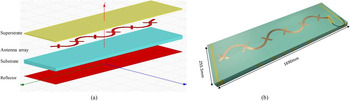
The final wideband antenna model was also fabricated and evaluated. The antenna was positioned between a substrate and a superstrate layer (see Fig. 10(a)) of polystyrene foam with a relative permittivity of 2.5 and a dielectric loss tangent equal to 0.029. The dimensions (length × width) of the foam were 1690.0 × 255.5 mm2, and the corresponding thickness was 28 mm for the substrate and 13.5 mm for the superstrate. Below the bottom (substrate) layer, a metallic foil of thickness equal to 0.3 mm was placed, which acts as a reflector of the array antenna. The electric properties of copper (with electric conductivity σ = 58 × 106 S/m) are selected for the printed array antenna and the reflector. A coaxial RF assembly with type-N (jack) connector is properly soldered to the antenna transformers without any matching device in-between, a task that needs to be performed in a careful way. This is something that should be taken into account from the designers that fabricate such kind of antennas. Figure 10(b) depicts the fabricated antenna array mounted on top of the substrate; the superstrate is not shown.
(a) The proposed antenna model design in layers (angled view); (b) photograph of the fabricated six-double-dipole array antenna (angled view).

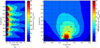
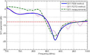
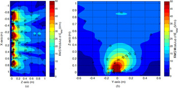
Figure 11 shows the electric field distribution (RMS total radiated electric field in V/m) of the final geometry of the wideband antenna at 867 MHz. The input power is set again to 30 dBm. As observed in the electric field results of the narrowband antenna, a semi-cylindrical volume that extends to a radius of more than 50 cm is sufficiently covered. The isoparametric lines of equal electric field are also included in Fig. 11, in order to identify the region of tag readability. Choosing once again a tag readability threshold of 5 V/m, we can show that any tagged item within this semi-cylindrical volume will be read and identified. Figure 12 depicts the simulated and the measured reflection coefficient (S11) of the fabricated wideband antenna as a function of frequency. The simulated results were extracted from the HFSS and SEMCAD commercial software and are in fairly good agreement. The measurements were carried out using Agilent E5062A vector network analyzer. Referring to Fig. 12, the center frequency of the antenna is slightly shifted by 13 to 880 MHz. Despite this, the operating bandwidth (RL > 13 dB) is about 93 MHz and covers a wide frequency range (847–940 MHz). As a conclusion, the measured return loss of the fabricated antenna meets the desired requirements and covers both the ETSI and the FCC frequency bands. It is pointed out that in [Reference Boursianis, Samaras, Polycarpou and Sahalos7] preliminary measurements were presented without numerical verification. In Fig. 12, the simulated and the measured results are depicted.
Electric field distribution (RMS values of the total radiated electric field in V/m) of the reader antenna array with N = 6 dipoles (d = 0.8λ at 867 MHz) and an input power of 30 dBm at 867 MHz (simulated results): (a) Vertical plane and (b) horizontal plane. Electric field values that are larger than 50 V/m are not distinguished in color scale. Red dash line refers to the semi-cylindrical volume with a radius of 50 cm.

The simulated and measured reflection coefficient (S11) versus frequency of the fabricated six-double-dipole wideband antenna array (blue solid line: FEM method, pink dot line: FDTD method, green dash-dot line: measurements, red dash line: −13 dB reference level).

Since the measured S11 of the fabricated antenna covers both the frequency bands of ETSI and FCC standards, it is also useful to examine the electric field distribution in the vicinity of the antenna at 930 MHz which is the upper frequency of the desired band. Figure 13 illustrates the RMS total electric field radiated from the antenna. Once more, it is obvious that a semi-cylindrical volume of a radius of 50 cm is still sufficiently covered. In all the cases of the designed and fabricated antennas a reflector was used. Owing to this, the coverage extends only in the front side of the antennas.
Electric field distribution (RMS values of the total radiated electric field in V/m) of the reader antenna array with N = 6 dipoles d = 0.8λ at 867 MHz) and an input power of 30 dBm at 930 MHz (simulated results): (a) Vertical plane and (b) horizontal plane. Electric field values that are larger than 50 V/m are not distinguished in color scale. Red dash line refers to the semi-cylindrical volume with a radius of 50 cm.

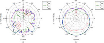
Finally, the radiation pattern (E-far field) of the antenna at 867 MHz is given in Fig. 14. The antenna gain is G = 11.9 dBi, the reflection coefficient is |Γ| = 0.193954 and the total efficiency is n = 94.4%.
The radiation pattern of the six-double-dipole antenna at 867 MHz: (a) Vertical plane; (b) Horizontal plane.

IV. SEARCHING FOR TAGGED ITEMS
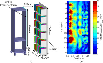
The designed six-double-dipole wideband antenna (Fig. 10(a)) is positioned in front of a metallic library cabinet with six shelves (Fig. 1) loaded with several tagged books. Figure 15(a) illustrates the geometry and the dimensions of the system, whereas Fig. 15(b) depicts the electric field coverage in the vicinity of the UHF RFID antenna at 867 MHz. The relative permittivity of the books is set equal to 3. Commercial RFID tags for libraries are usually embedded in the back of the book in the form of a wire; therefore, they are not expected to perturb significantly the field of the reader antenna. The distance between the reader antenna model and the library cabinet is set to 50 cm. As shown in Fig. 15(b), the coverage from the radiated electric field in the entire library cabinet model is quite satisfactory. Once again, if we choose a tag readability threshold of 5 V/m, we can easily deduce that any tagged book placed on the library shelves will be identified.
(a) The proposed wideband reader antenna model in front of a six-shelf library cabinet; (b) the electric field coverage (simulated results) of the reader antenna in front of a metallic library cabinet (input power = 30 dBm, tag threshold 5 V/m, XZ-plane – Y = 498 mm (center of the antenna)). Electric field values that are larger than 50 V/m are not distinguished in color scale.

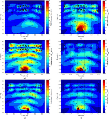
The same conclusion can be derived from the simulated results depicted in Fig. 16. Assuming that the tag power sensitivity is set to −14 dBm, and taking into consideration a worst-case scenario where 6 dB absorption occurs due to efficiency and de-polarization effects, the tag power sensitivity becomes −8 dBm [Reference Anabi, Mandeep, Islam and Tiang12]. Each of the six slices in Fig. 16 illustrates the field distribution in front and inside of the tagged books of the library cabinet. As it was already mentioned, the choice of 5 V/m ensures the detection of popular commercial tags [11]. From the preceding simulation results, it is clear that the tag readability threshold requirement of 5 V/m is met for all tagged books on the library cabinet regardless tag orientation.
The electric field (RMS values) coverage (simulated results) in front of the six shelves of the library. The slice in (a) refers to the bottom shelf. Electric field values that are larger than 50 V/m are not distinguished in color scale.

Measurements were also made in different vertical planes from 865 to 928 MHz using the fabricated wideband antenna prototype. The input power in all cases was set to 30 dBm. It was found that at a distance of 50 cm from the antenna axis, the electric field was between 10 and 20 V/m, well above the tag readability threshold of 5 V/m. The maximum value of the field was measured in the vicinity of the feeder at the lower position of the antenna. At a distance of 1 cm in front of the antenna, the electric field was between 50 and 100 V/m. It is understandable that for tags with better sensitivity the radiated power of the antenna can be proportionally reduced.
V. CONCLUSION
In this paper, two UHF RFID reader antennas for searching tagged items have been presented. The proposed antennas consist of a microstrip array with alternating orthogonal elements which are fed in series by a pair of microstrip lines. The line has a meander-shaped configuration that allows the elements to have the desired matching between the inter-element distance and phase difference. The bandwidth of the narrowband antenna is sufficient to cover only the ETSI standard, whereas the bandwidth of the wideband one covers both the ETSI and the FCC standards. The height of the wideband antenna is chosen to be approximately equal to the height of a typical cabinet of merchandise or books. The wideband antenna has been also analyzed and simulated in the presence of a library cabinet. Obtained simulation results have been presented and discussed in detail. Measurements of the reflection coefficient (S11) and simulated results of the governing E-field in the near-zone have shown that the proposed wideband antenna with the double dipoles can operate sufficiently in both ETSI and FCC frequency bands providing high percent readability and item identification.
ACKNOWLEDGEMENTS
The authors would like to acknowledge EU COST Action IC1301 Wireless Power Transmission for Sustainable Electronics.
FINANCIAL SUPPORT
This research is co-funded by the Republic of Cyprus through the Research Promotion Foundation (RPF) and the Structural Funds of the European Union (EU) under the grant with protocol number TΠE/OPIZO/0311(BIE)/03.
CONFLICT OF INTEREST
None.
 Anastasis C. Polycarpou graduated from Arizona State University in 1992 earning a BSEE degree in Electrical Engineering (EE) with Summa Cum Laude. He continued his graduate studies at the same University where he received an M.S. degree in 1994 and a Ph.D. degree in 1998. He is now a Professor and Department Head at the University of Nicosia in Cyprus. He has an extensive experience in funded research projects related to antenna analysis and design, microwave circuits and high-frequency electronic packaging, finite element/boundary integral methods in Electromagnetics, mode-matching and analytical methods, modeling of liquid crystals and non-linear optics, and radio frequency identification (RFID) systems. He is the author of a book and two chapters in books as well as a co-author of more than 80 papers in refereed journals and conference proceedings. Professor Polycarpou is a Senior Member of the IEEE and a member of IEEE Society on Antennas and Propagation and IEEE Society on Microwave Theory and Techniques. He is currently an Associate Editor of the IET Microwaves, Antennas & Propagation. He was a national delegate of COST IC0603 (ASSIST) and now a national delegate of COST IC1102 (VISTA). He is also a member of EurAAP.
 Achilles Boursianis was born in Larissa, Greece. He received his B.Sc. degree in Physics and M.Sc. degree in Electronic Physics – Radioelectrology (Electronic Telecommunications Technology), both from Aristotle University of Thessaloniki (AUTh), Greece. He is currently working toward a Ph.D. degree at the same University. He is also a research assistant with the Radio-Communications Laboratory, Department of Physics, AUTh. His research interests include analysis and design of optical networks, broadband monitoring systems, wireless sensor networks, and RFID antenna design. He is a member of the Hellenic Society of Physicists and the Electronic Physics Society.
 Theodoros Samaras has received his first degree and Ph.D. degree in Physics from Aristotle University of Thessaloniki, Greece and the M.Sc. degree in Medical Physics (with distinction) from the University of Surrey, Surrey, UK. He has worked in the Swiss Federal of Technology (ETH), and the Erasmus Medical Centre of Rotterdam, where he has conducted research on Computational Dosimetry for Electromagnetic Radiation. In December 1999, he returned to Aristotle University of Thessaloniki, where he is currently an Associate Professor. His research focuses on computer modeling for applications in biomedical technology and telecommunications. He was the recipient of a Marie-Curie Fellowship from the European Commission and is the author of several papers in peer-reviewed journals. He is currently member of the European Commission's Scientific Committee on Emerging and Newly Identified Health Risks (SCENIHR).
 Aggelos Bletsas is currently an Associate Professor at School of Electronic and Computer Engineering, Technical University of Crete. He received a diploma degree in Electrical and Computer Engineering from Aristotle University of Thessaloniki, Greece in 1998, and the S.M. and Ph.D. degrees in Media Arts & Sciences from MIT in 2001 and 2005, respectively. He worked at Mitsubishi Electric Research Laboratories, Cambridge, MA, and at Radiocommunications Laboratory, Department of Physics, Aristotle University of Thessaloniki. His research interests include detection and estimation, backscatter communications and RFID, energy harvesting, radio hardware/software implementations for wireless transceivers, and low cost sensor networks. Dr. Bletsas was the co-recipient of IEEE Communications Society 2008 Marconi Prize Paper Award in Wireless Communications, best paper distinction in ISWCS 2009, second best student paper award in IEEE RFID-TA 2011, and the best paper distinction in IEEE Sensors 2013. At the end of 2013, he was awarded the Technical University of Crete 2013 Research Excellence Award.
 John N. Sahalos is a Professor at the ECE Department of the University of Nicosia, Cyprus and a Professor Emeritus at the Aristotle University of Thessaloniki (AUTH), Greece. He was a visiting faculty member at the Ohio State University, the University of Colorado and the Technical University of Madrid. Author of four books and more than 450 articles published in the scientific literature. His research interests are in the areas of antennas, radio-communications, EMC/EMI, RFID, microwaves, and biomedical engineering. He is a member of the Board of Directors in a Multinational Telecommunications Company, executive manager of the UNIC Research Foundation (UNRF) and in the consulting committee of the GRNET. Dr. Sahalos is an IEEE Life Fellow, an Honorary Fellow of the Electronic Physics Society, a member of Physical Society and of the Technical Chamber of Greece. With his colleagues he designed innovative products such as the EIT, the MLS, the ORAMA simulator, and the SMS-K monitoring system.