Introduction
Ultrashort (femtosecond [fs]) laser pulses are a unique tool for materials processing, as their duration is shorter than the time required to transfer absorbed optical energy, via electron–phonon coupling, from the electronic system of the solid to its lattice. Hence the laser-pulse energy remains localized during the interaction and does not spread via diffusion into the area surrounding the irradiated region. The fs laser thus offers increased precision for material modification or ablation Reference Küper and Stuke1,Reference Srinivasan, Sutcliffe and Braren2 accompanied by a reduced heat-affected zone of only a few hundred nanometers. Reference Bonse and Krüger3 This confined heat-affected zone is more than an order of magnitude smaller than that typically reported for irradiation with longer, nano-, micro-, and millisecond laser-pulse durations. Reference Bäuerle4
From a physical point of view, the ultrafast interaction provides the means to drive the electronic system of the solid into a strong nonequilibrium state, triggering ultrafast phenomena such as bandgap collapse in semiconductors, Reference Glezer, Siegal, Huang and Mazur5 non-thermal melting, Reference Shank, Yen and Hirlimann6–Reference Zier, Zijlstra, Kalitsov, Theodonis and Garcia8 Coulomb explosion in a near-surface layer depleted of bonding electrons, Reference Stoian, Rosenfeld, Ashkenasi, Hertel, Bulgakova and Campbell9 and the excitation of collective electron modes (e.g., surface plasmon polaritons [SPPs]). Reference Bonse, Rosenfeld and Krüger10–Reference Murphy, Torralva, Adams and Yalisove12 Even if initiated by an ultrafast process, the subsequent material relaxation strongly affects the surface morphology as it can occur via a plethora of processes, including thermal melting, hydrodynamic melt flows, vaporization, phase explosion, structural modifications (amorphization/crystallization), or chemical reactions with the ambient environment (e.g., oxidation). Reference Bäuerle4,Reference Bulgakova and Bulgakov13–Reference Tsibidis, Barberoglu, Loukakos, Stratakis and Fotakis15 Moreover, repeated exposure of the same irradiated spot transforms roughened surfaces via interpulse feedback phenomena toward characteristic surface morphologies such as nanometric laser-induced periodic surface structures (LIPSSs), Reference van Driel, Sipe and Young16,Reference Reif, Costache, Henyk and Pandelov17 or micrometer-sized grooves and conical spikes. Reference Her, Finlay, Wu and Mazur18,Reference Tull, Carey, Mazur, McDonald and Yalisove19 The feedback mechanism during repetitive treatments selects specific spatial periods of the roughness distribution that can better absorb radiation. In other words, the first pulse generates a rough surface that facilitates the coupling of energy for the subsequent laser pulses.
Contour shaping of surfaces
Single-step contactless three-dimensional (3D) machining of contours on an arbitrary workpiece with nanometer precision has attracted the interest of scientific researchers and industrial engineers for decades. Many different processes have been developed for this, Reference Bäuerle4,Reference Sugioka and Cheng20 of which direct focusing of laser radiation is the most prominent. Using this technique along with high numerical aperture optics and taking advantage of nonlinear absorption in dielectrics at peak intensities >1013 W/cm2, surface craters and grooves of less than 50 nm were demonstrated using Nd:glass 800-fs-laser pulses at 1053 nm wavelength. Reference Joglekar, Liu, Meyhöfer, Mourou and Hunt21 Such high lateral resolution is achieved through the use of multiphoton absorption processes, required to bridge the bandgap energy along with a sharply defined ablation threshold, and the low electronic and thermal diffusivities confining the optical energy.
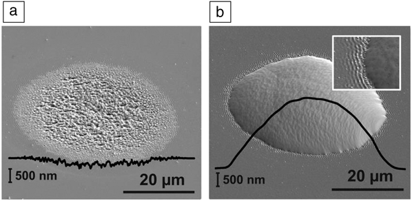
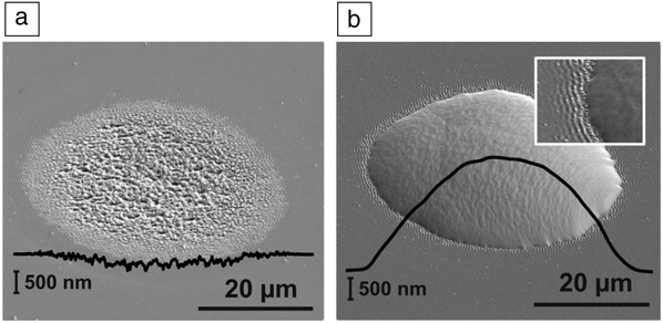
However, for many applications, larger contour sizes are desired. Figure 1 shows fs laser-based processing steps in the bottom-up manufacturing of chalcopyrite microconcentrator solar cells based on copper-indium-gallium-diselenide. Fs laser ablation of glass and a subsequent deposition of a molybdenum layer or direct-laser processing of the molybdenum film both allow the preferential nucleation and growth of indium islands at predefined locations in a subsequent indium-based physical vapor deposition process. It should be noted that a purely morphological surface modification is sufficient for the creation of preferential nucleation centers, whereas potential chemical surface modifications (laser-induced oxidation) do not affect the geometrically stimulated nucleation process. Reference Ringleb, Eylers, Teubner, Boeck, Symietz, Bonse, Andree, Krüger, Heidmann, Schmid and Lux-Steiner22 Interestingly, the inset in Figure 1b clearly demonstrates the presence of LIPSSs originally formed in the underlying glass substrate. Here, the whole glass substrate is covered by a molybdenum layer, and the indium starts to aggregate in the transition zone between the LIPSS and the surrounding surface region.
Microroughening of glass surface and subsequent site-selective material deposition of indium by physical vapor deposition (PVD). (a) Tilted-view scanning electron micrograph of soda-lime glass after 100 exposures of 30-fs laser pulse at a peak fluence of 1.6 J/cm2, resulting in a rough, 50-µm-diameter ablation crater with a depth of less than 300 nm (roughness R a ∼ 25 nm). The black curve represents a surface profile through the crater, taken by atomic force microscopy. (b) Similar laser ablation spot, homogeneously coated by a ∼400-nm-thick molybdenum film prior to the PVD of indium. The indium preferentially nucleates within the roughened spot and forms an island 2–3 µm in height. The black curve represents a profilometric scan across the center of the indium island. The inset in (b) provides a 9.4 µm × 7.4 µm detailed magnification of the indium–molybdenum transition zone, revealing laser-induced periodic surface structures in the underlying glass. Reference Ringleb, Eylers, Teubner, Boeck, Symietz, Bonse, Andree, Krüger, Heidmann, Schmid and Lux-Steiner22
Self-ordered surface structures
LIPSSs represent a universal phenomenon that occurs upon treatment of solids by laser radiation. Reference van Driel, Sipe and Young16,Reference Birnbaum23 For linearly polarized ultrashort laser pulses, two different types of LIPSSs have been reported in the literature: so-called low-spatial frequency LIPSSs (LSFL) with a periodicity (Λ) close to the irradiation wavelength (ΛLSFL ≈ λ) and high-spatial frequency LIPSSs (HSFL) with periods significantly smaller than λ (ΛHSFL << λ). For each specific type of LIPSS (LSFL and HSFL), the laser wavelength and the polarization are material-dependent key parameters for the resulting spatial characteristics of the nanostructures (i.e., their period is dictated by the irradiation wavelength and their orientation by the direction of the laser-beam polarization). Additionally, the energy density (fluence, in J/cm2) and the number of exposures (pulses) per spot can impose the type of LIPSS and affect their period.
For strongly absorbing materials such as metals or semiconductors, in most cases, LSFL is observed with orientation perpendicular to the laser-beam polarization. Reference Borowiec and Haugen24–Reference Bonse, Krüger, Höhm and Rosenfeld26 These LSFL are generated by interference of the incident laser beam with a surface electromagnetic wave generated at the rough surface, which might include the excitation of SPPs. Reference Bonse, Rosenfeld and Krüger10,Reference Huang, Zhao, Cheng, Xu and Xu11,Reference Bonch-Bruevich, Libenson, Makin and Trubaev27,Reference Sipe, Young, Preston and van Driel28
HSFL in semiconductors are a distinct LIPSS population that form through a different physical mechanism from the LSFL. The HSFL form via an additive mass redistribution of laser-generated Frenkel-like vacancy/interstitial pairs, not by laser ablation. Reference Abere, Torralva and Yalisove29 In GaAs, the HSFL form after irradiation with at least 1500 exposures within a range of fluences between 0.10 J/cm2 and 0.050 J/cm2 with an average period of 180 nm, as shown in Figure 2b. LSFL form above the melt threshold (Figure 2a), while no morphological changes occur even after 106 exposures below this range (Figure 2c). The sharp HSFL formation threshold is independent of both laser-spot size and the exposure number, Reference Abere, Torralva and Yalisove29 which indicates that the vacancy/interstitial pairs are not generated through a purely thermal mechanism. In fact, the vacancy/interstitial pairs responsible for HSFL are generated due to the unique dynamics of the lattice’s response to ultrafast laser excitation.
Measured thresholds in GaAs. (a) Low-spatial frequency laser-induced periodic surface structures (LSFL) form after 200 exposures above the melt threshold at 0.10 ± 0.01 J/cm2 with period 620 nm. Additional exposures do not produce high-spatial frequency laser-induced periodic surface structures (HSFL). (b) HSFL with period 180 nm formed after 1500 exposures at a peak fluence of 0.065 ± 0.005 J/cm2. (c) No morphological changes occur below 0.050 ± 0.005 J/cm2. Error represents day-to-day variation in the threshold measurements. HSFL formation is observed at fluences where irradiation initiates bandgap closure without melting the material, the conditions necessary for ultrafast laser-induced point defect generation. Reference Abere, Torralva and Yalisove29 Note: E, direction of the laser-beam polarization.

During an ultrashort laser interaction, the bonding states of a semiconductor are depopulated, which weakens the attractive part of the interatomic potential and allows ions that are formed to drift with their initial thermal momentum. Seminal x-ray diffraction experiments, Reference Rousse, Rischel, Formaux, Uschmann, Sebban, Grillon, Balcou, Förster, Geindre, Audebert, Gauthier and Hulin7,Reference Lindenberg, Larsson, Sokolowski-Tinten, Gaffnery, Blome, Synnergren, Sheppard, Caleman, MacPhee, Weinstein, Lowney, Allison, Matthews, Falcone, Cavalieri, Fritz, Lee, Bucksbaum, Reis, Rudati, Fuoss, Kao, Siddons, Pahl, Als-Nielsen, Duesterer, Ischebeck, Schlarb, Schulte-Schrepping, Tschentscher, Schneider, von der Linde, Hignette, Sette, Chapman, Lee, Hansen, Techert, Wark, Bergh, Huldt, van der Spoel, Timneanu, Hajdu, Akre, Bong, Krejcik, Arthur, Brennan, Luening and Hastings30,Reference Fritz, Reis, Adams, Akre, Arthur, Blome, Bucksbaum, Cavalieri, Engemann, Fahy, Falcone, Fuoss, Gaffney, George, Hajdu, Hertlein, Hillyard, Horn-von Hoegen, Kammler, Kaspar, Kienberger, Krejcik, Lee, Lindenberg, McFarland, Meyer, Montagne, Murray, Nelson, Nicoul, Pahl, Rudati, Schlarb, Siddons, Sokolowski-Tinten, Tschentscher, von der Linde and Hastings31 which confirmed previous theoretical work, Reference Graves and Allen32 show that these ions are capable of drifting as much as an angstrom within a few hundred fs before colliding with nearby ions. These collisions result in loss of the long-range order of the crystal within a picosecond for fluences above the melt threshold. Just below the melt threshold, this atomic motion is sufficient to temporarily change GaAs into a centrosymmetric state Reference Glezer, Siegal, Huang and Mazur33 and induce bandgap closure.
The fluence range over which GaAs exhibits bandgap closure without melting Reference Sundaram and Mazur34 is equivalent to the HSFL formation conditions in Figure 2. Although semiconductors appear to completely recover their original dielectric properties after a single laser exposure with no surface morphological change at these fluences, the Maxwellian distribution of the room-temperature thermal momentum ensures that some atoms will have the initial conditions to reach an interstitial site. The resulting configurational change to form a vacancy/interstitial pair then acts as a nonradiative pathway for electrons to reoccupy the bonding states.
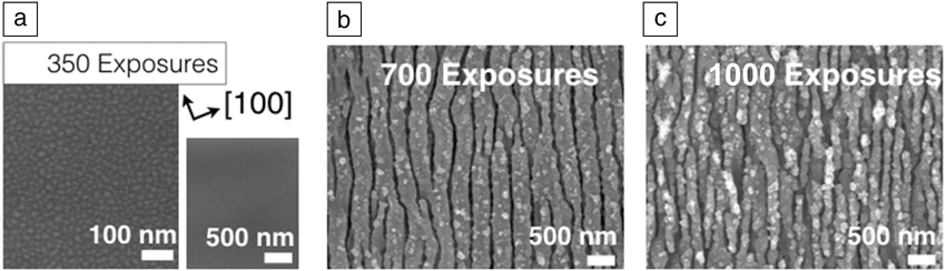
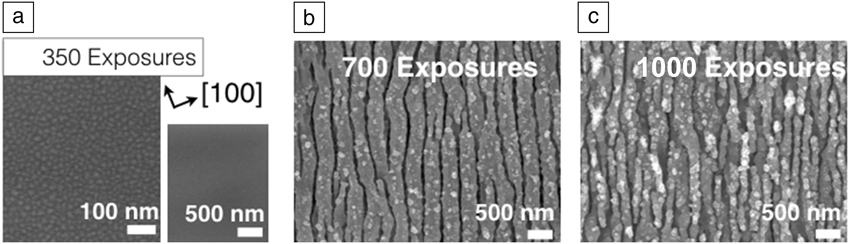
Ultrafast laser irradiation over multiple repeated exposures builds up a sufficient vacancy/interstitial population, which leads to rapid diffusion of the self-interstitials to form a random distribution of islands, 20 nm in diameter, as shown in Figure 3a. When the light couples to the surface plasmons to form SPPs at the roughened surface, vacancy/interstitial pairs are preferentially generated where the field is locally the most intense, which is consistent with the observed mass redistribution into periodic structures oriented perpendicular to the laser polarization at a 355 nm period Reference Huang, Zhao, Cheng, Xu and Xu11,Reference Barnes, Preist, Kitson and Sambles35 as seen in Figure 3b. The LIPSSs bifurcate to the 180 nm HSFL in Figure 3c, a period shorter than would be attainable through a purely SPP-based process, via the relaxation of tensile stress from the slower diffusing vacancies within the near surface. Reference Abere, Torralva and Yalisove29,Reference Yang and Srolovitz36
GaAs morphology in a scanning electron micrograph after ultrafast laser irradiation at a fluence of 0.065 ± 0.005 J/cm2 after (a) 350 exposures (left) at a magnification to show features and (right) one to show on a consistent scale with; (b) 700; and (c) 1000 exposures showing the initial islands and then bifurcation of laser-induced periodic surface structures from (b) 355 nm to (c) 180 nm. Reference Abere, Torralva and Yalisove29
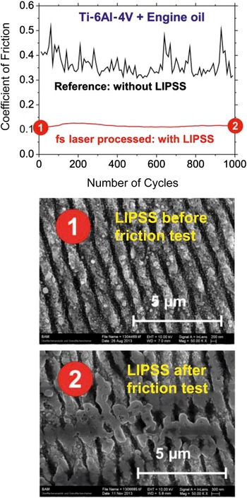
Several applications of LIPSSs have recently gained attention, including surface colorization and the control of surface-wetting properties. Reference Vorobyev and Guo25 The beneficial tribological performance of fs laser-generated LIPSSs on a titanium alloy surface is illustrated in Figure 4 . Reference Bonse, Koter, Hartelt, Spaltmann, Pentzien, Höhm, Rosenfeld and Krüger37 The upper graph shows the coefficient of friction (COF) versus the number of sliding cycles in a reciprocating sliding tribological test (RSTT) with a 10-mm-diameter ball of hardened 100Cr6 chrome steel moving in a commercial engine oil against a LIPSS-covered Ti-6Al-4V surface (red curve) or against a polished Ti-6Al-4V reference surface (black curve). While the polished surface exhibits a COF ranging from ∼0.3 to ∼0.5 during 1000 sliding cycles, in the LIPSS-covered regions, the COF is reduced by a factor of more than two (i.e., ∼0.12 to ∼0.14). As indicated by the scanning electron micrographs of LIPSSs acquired before (labeled “1”) and after (labeled “2”) the tribological test, these nanostructures (having a depth modulation of typically a few hundreds of nanometers) clearly endure the RSTT treatment (see the lower part of Figure 4).
Tribological performance of fs LIPSSs (laser-induced periodic surface structures) on titanium alloy (Ti-6Al-4V). Regime of mixed friction: normal force 1 N, stroke length 1 mm, frequency 1 Hz, lubricant engine oil. Top: coefficient of friction (COF) versus number of sliding cycles indicating a reduction of the COF at the laser-induced periodic surface structure covered surfaces by more than a factor of two. Middle and bottom: scanning electron micrographs before (labeled “1”) and after (labeled “2”) the tribological test, respectively. Reference Bonse, Koter, Hartelt, Spaltmann, Pentzien, Höhm, Rosenfeld and Krüger37

Hierarchical micro- and nanostructures
Through ultrafast laser direct writing, diverse micro-nanostructures can be produced on bulk solid surfaces via different laser–matter interaction mechanisms. Briefly, surface micro-nanostructures are mainly formed via two processes: the laser-inscribing process to form ordered microscale structure arrays and the laser-inducing process to form nanoscale as well as disordered microscale structures. Reference Fan, Zhong, Li, Huang and Zhang38–Reference Fan, Zhong, Bai, Jin and Zhang41 During laser inscribing, material ablation and removal occurs within the irradiated spot, which leaves various periodic microscale patterns depending on the specific laser-machining routine. Conversely, the laser-irradiation process may drive self-organization of surface structures with dimensions much smaller than the beam diameter or spatial distributions that are obvious departures from the laser-inscribed features. Hierarchical features can exist on surface structures produced via either mechanism. For example, arrayed microscale structures are usually covered with submicron corrugations, while disordered microscale structures are decorated by particles of varied dimensions.
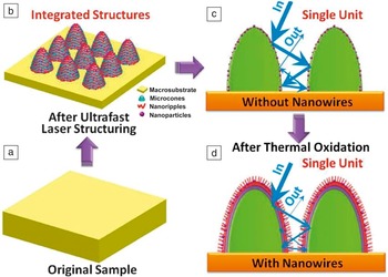
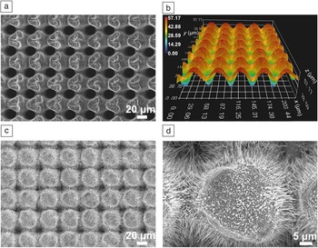
When the top-down ultrafast laser direct-writing approach is combined with bottom-up thermal oxidation growth, an ultrafast laser hybrid nanomanufacturing strategy can be carried out with the advantage of facilely producing various 3D self-supporting nanowires in situ on bulk metal substrates. Reference Fan, Bai, Long, Jiang, Jin, Zhang and Zhong40,Reference Fan, Zhong, Bai, Jin and Zhang41 Ultrafast laser direct writing is first implemented to produce specific micro-nanostructures on metal surfaces (e.g., the microcone arrays covered with nanoripples and nanoparticles, see Figure 5b), which serve as the precursors for driving subsequent growth of oxide nanowires under thermal oxidation (Figure 5c–d). Additionally, preexisting micro-nanostructures can facilitate and accelerate the oxide nanowire growth. The bulk-metal substrate, the ultrafast laser directly written micro-nano features, together with the oxide nanowires, can combine to form a macro-micro-nano-nanowire multiscale hierarchical structure. It is composed of metallic micro-nano features as well as semiconductor oxide nanowires, and is a good candidate for applications demanding any combination of metal and semiconductor. For applications such as antireflective coatings, ultrafast laser-fabricated microstructures can play the role of light trapping, while the nanowires can enhance optical phonon dissipation, resulting in significantly improved antireflection performance.
Schematic of the ultrafast laser hybrid nanomanufacturing strategy. (a) Original bulk metal sample. (b) Microcone arrays formed after ultrafast laser structuring. (c) Single unit of the microcone arrays. (d) Single unit of the microcone arrays with nanowires grown after thermal oxidation. Blue arrows in (c–d) represent the traveling of incident light among the microcones. Reference Fan, Bai, Long, Jiang, Jin, Zhang and Zhong40

Under optimized ultrafast laser-processing parameters, uniformly distributed microcone arrays have been fabricated on Cu surfaces, as shown in Figure 6a, Reference Fan, Bai, Long, Jiang, Jin, Zhang and Zhong40 with each cone having clear contour profiles (Figure 6b). After growing oxide nanowires through thermal oxidation, the microcones become fluffy, as seen in Figure 6c. The nanowires radially grow from the outer surface of the cones into the free space with a dense and uniform distribution, reaching lengths of more than 10 μm (Figure 6d). The relatively large-scale microcones serve as a bridge connecting the oxide nanowires to the bulk-metal substrates and the skeleton to support the integrated surface architectures. The nanowires and the precursor structures are neatly combined, showing no obvious interface characteristics, making the constructed architectures a robust structural system.
Characterization of the micro-nanostructures as well as nanowires. (a–b) Scanning electron microscope (SEM) and 3D optical microscope images for ultrafast laser fabricated micro-nanostructures. The color bar encodes the surface height (z) ranging from 0–57.17 µm. (c–d) SEM images for micro-nanostructures with nanowires in low and high magnification. Reference Fan, Bai, Long, Jiang, Jin, Zhang and Zhong40

In addition, the properties of oxide nanowires are dependent on the type of precursor structure. Since the precursor structures can be controlled by tuning the laser-irradiation parameters, the hybrid strategy can actually provide a facile method to form nanowires with desired distribution, and the fabrication of more complex and user-definable 3D architectures can be realized. For instance, 1D periodic structures, particle cluster structures, and vivid helical structures can be separately fabricated by ultrafast laser direct writing. In spite of the strikingly different forms of these structures, oxide nanowires have been grown on each precursor geometry. Reference Fan, Zhong, Bai, Jin and Zhang41
Based on this, the physical and chemical properties of the macro-micro-nano-nanowire hierarchical structures can be flexibly tuned. In particular, ultralow hemispherical reflectance of 0.6% has been reached in the mid-infrared spectrum, Reference Fan, Bai, Long, Jiang, Jin, Zhang and Zhong40 exhibiting great potential in fields such as thermal imaging, sensors, and stealth. More importantly, ultrafast laser direct writing is a unique technique with no apparent material dependence; meanwhile, thermal oxidation has proven effective in synthesizing different kinds of metal oxide nanowires. In this regard, the hybrid manufacturing strategy can also be applicable in creating 3D multiscale architectures on other metal substrates, offering a general and convenient route for fabricating complex 3D hierarchical components for different functional devices. Reference Fan, Zhong, Bai, Jin and Zhang41
Outlook
Morphological transformations upon ultrashort laser pulse processing have already reached an advanced research state and are currently entering industrial applications, such as in microscale photovoltaics, enhancement of tribological performance, surface colorization, control of wetting and (cell and bacterial) adhesion properties, and cutting of display glasses.
In academic research, the current trend is to use even shorter pulse durations approaching the attosecond range. However, the applicability of sub-fs laser pulses to laser surface processing is still hampered by the complexity of the laser system and beam delivery, including, for instance, limited pulse energy at suitable laser wavelengths and pulse distortion and prolongation effects.
In industry, at present, pulse durations of a few hundred fs are favored for robust materials processing. Here, a trend toward ever higher pulse repetition rates in combination with advanced laser scanning technology is emerging. However, at multi-MHz repetition rates, scan velocities at the ∼100 m/s level and intelligent processing strategies are required to benefit from the ultrafast laser pulse durations. The fast and smart scanning helps to avoid or control thermal heat accumulation when the surfaces cannot sufficiently cool down between successive laser pulse exposures.
Acknowledgments
M.J.A.’s contributions to this work were supported by the Air Force Office of Scientific Research Contract No. FA9550–12–1-0465 at the University of Michigan. M.J.A. is currently affiliated with Sandia National Laboratories, which is a multiprogram laboratory managed and operated by Sandia Corporation, a wholly owned subsidiary of Lockheed Martin Corporation, for the US Department of Energy’s National Nuclear Security Administration under Contract DE-AC04–94AL85000.

Michael J. Abere is currently at Sandia National Laboratories. He received his PhD degree in materials science and engineering from the University of Michigan in 2015 while studying ultrafast laser-driven nanostructure self-assembly. His research focuses on direct laser and shock, via laser flyer, induced ignition of reactive nanolaminate foils. Abere can be reached by phone at 505-844-5282 or by email at mjabere@sandia.gov and mjkabere@gmail.com.

Minlin Zhong is a professor in the School of Materials Science & Engineering at Tsinghua University, China. He earned his bachelor’s degree in 1983, master’s degree in 1990, and PhD degree in 1997. He is currently an executive board member of the Laser Institute of America (LIA) and president of the International Academy of Photonics and Laser Engineering (IAPLE). He is a Fellow of LIA and IAPLE. His research interests include laser micro-nanofabrication, surface engineering, and additive manufacturing. He has published more than 300 papers. Zhong can be reached by phone at +86-10-62772993 or by email at zhml@tsinghua.edu.cn.

Jörg Krüger is currently acting head of the 6.4 Nanomaterial Technologies Division at the Federal Institute for Materials Research and Testing (BAM). He received his diploma and doctoral degree in physics from the Friedrich-Schiller-University Jena and the Brandenburg University of Technology Cottbus, Germany. His research interests include ultrashort pulse laser materials processing, laser applications for the preservation of the cultural heritage, and laser safety issues. He is a co-author of more than 150 publications. Krüger can be reached by phone at + 49 30 8104-1822 or by email at joerg.krueger@bam.de.

Jörn Bonse is a senior scientist at the Federal Institute for Materials Research and Testing (BAM), Germany. He received a PhD degree and a diploma in physics and occupied research positions at the Max-Born-Institute, the Spanish Research Council (CSIC), and the Laser Zentrum Hannover. He was a senior laser application specialist at Newport Spectra-Physics, received several research awards, and currently serves as an associate editor for Optics Express. His research interests include fundamentals and applications of laser–matter interactions. Bonse can be reached by phone at + 49 30 8104-3562 or by email at joern.bonse@bam.de.