I. INTRODUCTION
Since the demand for high–speed data transmission has exponentially grown over the last few decades and is still growing rapidly, new solutions for high–speed data transmission systems attract a great deal of interest. Due to the massive spread of mobile media devices this growth develops with an enormous speed in the resorts of mobile data services such as high–quality multimedia streams, mobile high–definition television, and mobile internet resulting in increased requirements for base station backhauling networks, especially in terms of data rate. Multi-gigabit-class wireless links appear as an attractive extension for fiber optical connections to provide last mile access, radio backhauling, and bridging optical networks over short distances in adverse terrain. To achieve the required capacities and bandwidths, the efficiency of existing wireless data links have to be enhanced by either increasing the absolute bandwidth or by using increasingly complex modulation techniques, such as multiple quadrature amplitude modulation, which comes along with a huge amount of baseband data processing and even more complex requirements on the design of modulation circuits.
Wireless communication systems set up using millimeter-wave (MMW) technologies are perfectly suitable for increasing the data rate of such links, because the exploitable absolute bandwidth increases with the carrier frequency. Therefore, we propose the use of frequencies in the 220–325 GHz band for wireless access systems to overcome the bandwidth insufficiency. This frequency band is well suited for communication and data transmission applications because of the high available bandwidth as well as the relatively low path losses due to the atmospheric attenuation window. Communication systems in this regime could handle data rates well in excess of 12.5 Gbit/s, today's limit of demonstrated wireless data rates. In addition to the multi-Gbit data rate, the size of such systems will reduce significantly with the use of millimeter wave monolithic integrated circuits (MMICs), leading to more compact and more cost-effective systems. By pushing the carrier to even higher frequencies even more bandwidth is available, enough to equal the data rate of 40 Gbit/s in today's optical communication systems.
Up to now, state-of-the-art wireless communication systems in the high MMW frequency range between 200 and 300 GHz are realized by passive electronics, i.e. Schottky diodes or by optical and opto-electrical systems. First experiments at a carrier frequency of 300 GHz using sub-harmonic Schottky mixers show promising results for the transmission of high–data–rate digital video signals with data rates up to 96 Mbit/s [Reference Jastrow1]. The combination of optical and opto-electrical systems together with a direct detection receiving scheme allows data rates of up to 10 Gbit/s at frequencies of 120 [Reference Kukutsu2, Reference Yamaguchi3] and 250 GHz [Reference Song4]. As shown in [Reference Song5] data rates up to 12.5 Gbit/s are transmitted at 300 GHz over a distance of 0.5 m. In lower–frequency regimes also MMIC–based systems are reported.
In this paper, we present the characterization of MMIC modules suitable for a wireless data transmission at a carrier frequency of 220 GHz. The MMICs are fabricated in a 50 nm gate length metamorphic high electron mobility transistor (mHEMT) technology with a f t and f max of 375 GHz each [Reference Leuther6] and packaged into split-block waveguide modules allowing easy setup and handling. Using these components we demonstrate wireless data transmission of pseudo-random binary sequence (PRBS) signals at data rates up to 12.5 Gbit/s over a transmission distance of 2 m as well as the transmission of DVB-S real-time TV over a distance of 20 m.
The paper is outlined as follows: In Section II, the building blocks as well as the MMIC components of the wireless link are described. Subsequently, in Section III, the characterization of the receiver sensitivity is shown. Section IV details the transmission experiments using eye-diagram measurements and bit error rate measurement using a bit error detector for a transmission distance of 2 m as well as the setup for the 20 m real-time DVB-S TV transmission.
II. MMIC-BASED TRANSMIT AND RECEIVE FRONTEND
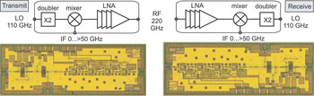
The wireless data link is set up using single-chip receiver and transmitter solutions housed in split-block waveguide modules. Both the receiver and transmitter chip use identical frequency multiplication and conversion stages. The frequency conversion is realized by a bi-directional resistive mixer, whose local oscillator signal is provided via a frequency doubler. A four-stage low-noise amplifier (LNA) at the input of the receiver chip provides 20 dB of small-signal gain at the RF path. In the transmitter, the same four-stage LNA is used as post-amplifier to the mixers RF signal, providing a transmit power up to 0 dBm. The used four-stage LNA was designed to achieve high gain and large bandwidth in combination with low noise figure. Therefore, a cascode configuration was utilized. The chip performance and measurement results are published in [Reference Tessmann7]. Figure 1 shows block diagrams and corresponding chip photos of the receiver and transmitter MMICs. Since the only difference in the circuit architecture of the transmitter and the receiver is the mirrored LNA placement, it is possible to carry out both MMICs with identical chip size and interconnect interface at all ports. Moreover, the frequency characteristics of the transmitter and receiver are perfectly matched to each other, i.e. the mixer's LO port matching toward the frequency doubler as well as the mixer's bandwidth and conversion behavior is identical in both modules. The former assures that both mixers work with exactly the same LO power, the latter is important for optimum data transmission characteristics in terms of data and error rate. The MMICs are fabricated in a 50 nm mHEMT technology with a f t and f max of 375 GHz each [Reference Leuther6]. The circuits are realized using grounded coplanar transmission lines with a ground-to-ground spacing of 14-µm for optimal wave guidance paired with small chip size.
Block diagram and chip photos of the single-chip transmit and receive MMICs with a frequency doubler which provides the 220 GHz LO signal for the resistive mixer's LO port. Additionally a four–stage LNA is placed at each mixer's RF port. The chip size of each MMIC is 0.75 × 2 mm2.

The MMICs are mounted into split-block waveguide modules, which provide WR-10 (75–110 GHz) waveguide interfaces for the LO ports, as well as WR-3 (220–325 GHz) waveguides at the RF ports. The IF signal is routed via a coaxial 50 Ω 1.85 mm connector to provide broadband performance. Additionally, the chips' DC-supply board is included at the backside of the module, which generates all the necessary voltages for the MMIC from a single 5 V supply. The gate and drain supply voltages of the MMIC's subcircuits can be controlled separately. The transmit and receive modules' performance together with first DVB-C transmission experiments are published in [Reference Kallfass8].
III. DATA LINK CHARACTERIZATION
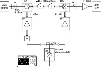
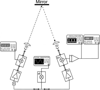
The described MMIC components are used to realize a wireless data link capable of transmitting data rates up to 12.5 Gbit/s. To investigate the potential as well as the maximum achievable data rate for the frontend modules, the input sensitivity of the receiver module is measured. A schematic of the link setup is shown in Fig. 2. The LO-frequency for both modules is generated using a single commercial W-band source module. This signal is split via a magic-tee and fed to two in-house power amplifiers, delivering the required power level of 11 dBm to drive the transmitter's and receiver's sub-harmonic LO-ports. To provide coherent up- and down-conversion a W-band phase shifter is included in the transmitter's LO path to adjust the LO phase. This is required because both mixers are single-ended. A double-sideband, zero-IF transmission with an incoherent LO signal at the receiver with respect to the transmit-LO could results in a defective IF signal or in the worst case even in IF signal cancellation. The baseband data signal at the transmitter is fed to the IF port via a bias-tee with a lower cut-off frequency of 50 kHz and is up-converted to the RF frequency range around 220 GHz. The receiver's down-converted IF signal is post-amplified by two cascaded broadband amplifiers to meet the input requirements of the measurement equipment. The amplifier chain provides a gain of approximately 42 dB with a lower cut-off frequency of 200 kHz.
Measurement setup for the characterization of the receiver module.

The transmit and receive modules are connected using WR-3 waveguide components. To control the receiver input power, two WR-3 attenuators are installed in between these waveguide components. The actual receiver input power for each data rate and adjustment of the WR-3 attenuators is measured using a power meter with an attached diode detector. Therefore, the measurement is limited to approximately −39 dBm due to the minimum input power requirements by the detector. An on–off–keyed PRBS with a length of 27 − 1 is used as a data signal for the transmit module. It is generated using a bit pattern generator (BPG) with a tunable data rate from 1 to 12.5 Gbit/s. At the receiver's IF port a digital communication analyzer is used to evaluate the quality of the transmission by means of eye diagrams, a bit error rate tester (BERT) is used to determine the errors introduced due to the transmission. Since the input of the BERT is limited to an input level between 0.5 and 2 V, the input level has to be adjusted by using appropriate additional attenuation in the IF path. To meet the BERT's input requirements in terms of maximum input amplitude, the attenuation between the amplifier chain and the BERT input is changed. However, higher attenuation results in a lower eye opening leading to measurements closer at the edge of the BERTs input sensitivity. Therefore changes at the BERT's input level result in slightly different appearance of the eye diagrams as well as changes in the measured sound to noise ratio (SNR) value.
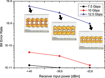
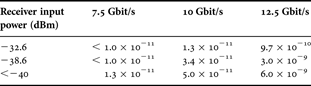
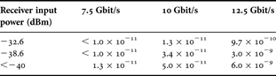
At a data rate of 7.5 Gbit/s, a bit error rate better than 1.0 × 10⁻¹¹ is obtained at a received power of −38.6 dBm. Measurements at data rates of 10 and 12.5 Gbit/s at these received power level show error rates of 3.4 × 10⁻¹¹ and 3.0 × 10⁻⁹, respectively. Measurements with a higher attenuation are performed but because of the power meter limitation mentioned above the exact input power value cannot be verified. The additional attenuation is approximately 3 dB compared to the −38.6 dBm measurement. Figure 3 shows the receiver sensitivity characteristics including the corresponding eye diagrams at a data rate of 12.5 Gbit/s, Table 1 shows the result of each BER measurement.
BER characteristics of a 7.5, 10, and 12.5 Gbit/s OOK signal transmission. The transmitter and receiver module are connected via waveguides. The eye diagrams show the eye opening for a data rate of 12.5 Gbit/s.

Results of receiver sensitivity measurements for a pattern length of 27 − 1.
IV. TRANSMISSION EXPERIMENTS
To demonstrate the capability of the wireless link, experiments for different transmission distances were performed. Since the transmitter and receiver module are fed by the same LO source due to the leg of a carrier recovery at 220 GHz, the modules have to be situated next to each other. To perform transmission for distances above 50 cm, the experiments are non line-of-sight. Therefore, the transmitter and receiver modules were aligned with a metallic mirror in such a way that the transmitted signal is inline with the receiver, see Fig. 4. To simplify the alignment and to reduce the path loss, we use high–density polyethylene (HDPE) lenses producing a collimated beam.
Measurement setup of the wireless data link for non line-of-sight characterization.

A) Measurements for 2 m transmission distance
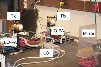
For the first experiment, a transmission distance of 2 m is chosen, thus the distance between the metallic mirror and the transmitter and receiver unit is 1 m. In this experiment, we use lenses that are optimized for a frequency of 325 GHz with Zemax®, a commercial ray-tracing program normally used in the optical domain. The lenses can also be used in the frequency range around 220 GHz by adjusting the position of the feeding horn antenna in the lenses focal points. The diameter of the lenses is approximately 70 mm. The antenna gain of the lenses–feed horn antenna combination, which is integrated into one module, is approximately 25 dBi. The transmit and receive modules with the attached lenses are mounted onto a dovetailed rail for horizontal alignment. The vertical alignment is realized by optical lense carriers which allow a coarse adjustment using a fixing screw. Figure 5 shows a photograph of the experiment setup showing the Tx/Rx-mirror alignment as well as the LO source and distribution. In order to determine the quality of the data transmission, eye-diagram and bit error rate measurements were performed. The results are shown in the following sections.
Photo of the experiment setup for 2 m data transmission showing the LO generation and PAs as well as the Tx/Rx-mirror alignment.

1) EYE-DIAGRAM MEASUREMENTS
For the eye-diagram measurements an Anritsu MP1758A BPG is used to provide a 231−1 word length PRBS that is used as an input signal for the data link characterization. The BPG can generate data rates up to 12.5 Gbit/s at four independent channels. The output amplitude and offset for the output signal can be adjusted separately for each channel. The output amplitude of the BPG is adjusted in a way that the corresponding input power at the transmitter module is 3 dBm. The output signal of the receiver module is fed to one of the input channels of an HP83480A Digital Communication Analyzer combined with an HP54752A two-channel 50 GHz module. The analyzer is triggered by the BPGs trigger output to the 1/32 clock. A second output from the BPG is directly fed to the analyzer for reference purpose.
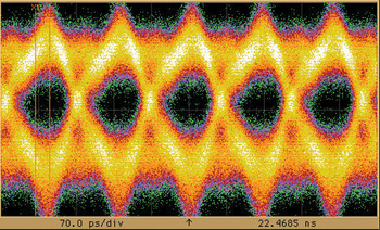
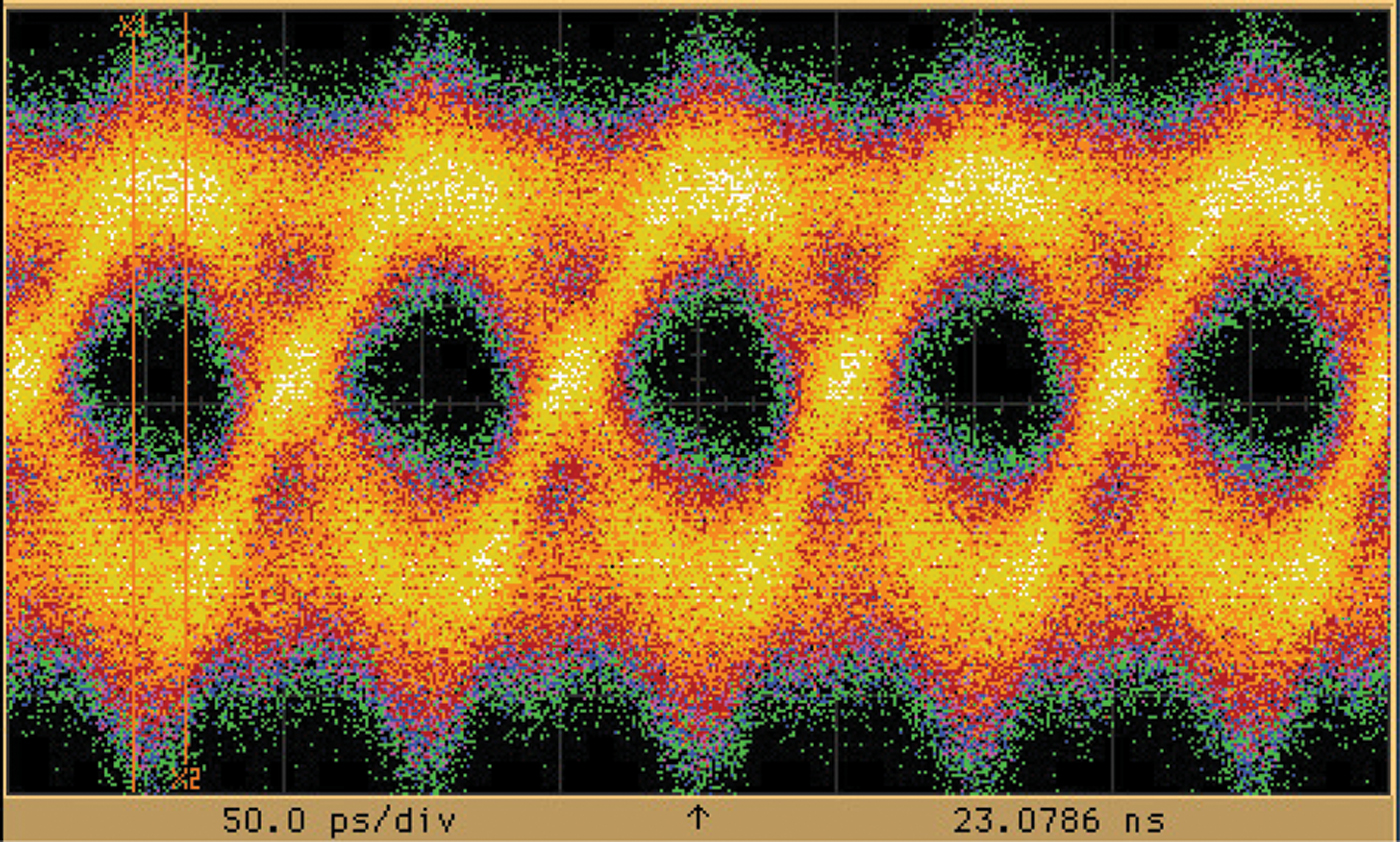
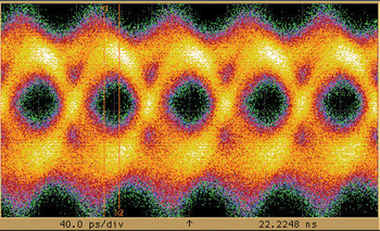
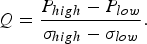
The resulting eye-diagrams for data rates of 7.5, 10.0, and 12.5 Gbit/s are shown in Figs. 6–8, respectively. The eye-diagrams are analyzed in terms of the quality factor Q, which is a measure of the vertical eye opening relative to the noise at both the high- and low- logic levels. If Phigh/low describes the mean value of the measured high and low levels and σhigh/low describes their standard deviations the Q-factor can be expressed as
Eye-diagram for a data rate of 7.5 Gbit/s with a q-factor of 3.55 over a distance of 2 m.

Eye-diagram for a data rate of 10 Gbit/s with a Q-factor of 3.58 over a distance of 2 m.
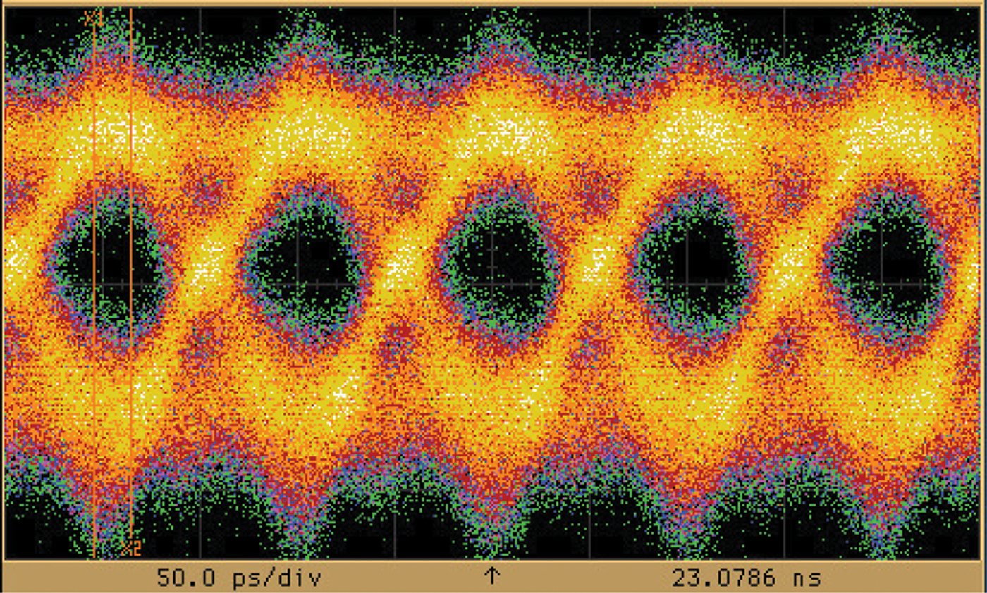
Eye-diagram for a data rate of 12.5 Gbit/s with a Q-factor of 3.59 over a distance of 2 m.

The measured Q-factors of the 7.5, 10, and 12.5 Gbit/s data transmission are 3.55, 3.58, and 3.59, respectively. The corresponding eye heights, which is an important measure to determine the input sensitivity of following data processing stages, are 37 mV for the 7.5 Gbit/s signal and 32 mV for both the 10 Gbit/s, and the 12.5 Gbit/s signal.
2) BIT ERROR RATE MEASUREMENTS
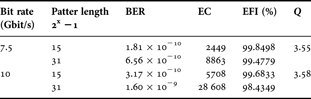
For the bit error rate measurements the BPG setup is equal to that for the eye-diagram measurements. To evaluate the bit errors introduced by the data link we use an Anritsu MP1764A bit error detector, which is triggered by the BGP's trigger output. The BER is measured for data rates of 7.5 and 10 Gbit/s for a pattern length of 215 − 1 as well as for a pattern length of 231 − 1. The results are as follows: for a pattern length of 215 − 1 the bit error rates are 1.81 × 10⁻¹⁰ for a data rate of 7.5 Gbit/s and 3.17 ×10⁻¹⁰ for a data rate of 10 Gbit/s. For the 231 − 1 pattern the bit error rates are 6.56 × 10⁻¹⁰ and 1.60 × 10⁻⁹, respectively. Each bit error rate measurement was performed for a time period of 30 min to get meaningful results. To assure that the measured bit error rates are correct, additional bit errors can be introduced at the BPG. If the error detector detects those manually introduced errors one can assume that the measurement is correct. Table 2 shows a summary of the measurement results expressed in terms of BER, error count over the measurement period and, corresponding to that, the error free interval ratio. The error–intervals (EI) describe the number of intervals containing one or more error pulses in measurement time. The error-free intervals (EFI) ratio is the ratio of the total number of intervals to the number of intervals containing one or more error pulses in measurement time. It is calculated from the number of EI with the following equation:

Results of bit error rate measurements for a transmission distance of 2 m.
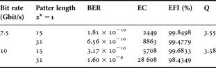
The table also shows the Q-factors calculated from the eye diagram by the Digital Communication Analyzer introduced in Section I. The reason for the increased error rate for the longer pattern could be explained by bit errors introduced by the lower cut-off frequency of the bias-tees and broadband amplifiers. For long bit patterns there are very long sequences of high or low values corresponding to a low frequency. The influence of the PRBS length cannot be seen in the measured Q-factors since the measurement period was so short that the changes in the eye-diagram due to the increased high and low sequences is small compared to the overall noise.
B) Measurements for 20 m transmission distance
To achieve higher transmission distances a new pair of HDPE aspherical plano-convex lenses is designed. These lenses are optimized for a frequency range around 220 GHz. A simulation with Zemax® predicts a gain of approximately 32 dBi for the lenses in combination with a 15 dBi feed horn. Since there are no measurements for the refraction index of HDPE available at frequencies above 160 GHz, the index is extrapolated from existing data. We assume a refraction index of 1.5245 at 220 GHz. The diameter of the new lense is 103 mm at a thickness of 15 mm, the focal point is 230 mm away from the center of the lense.
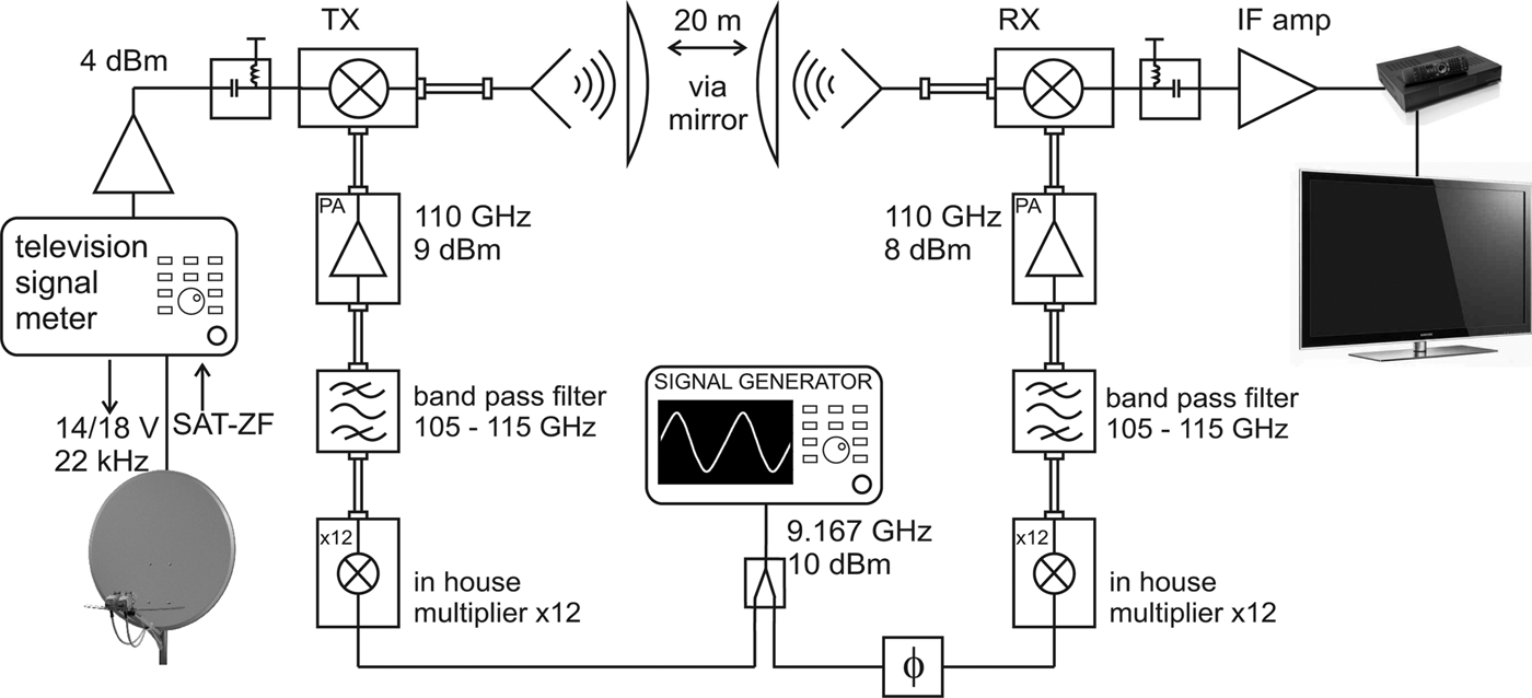
To build a more compact and easy to deploy setup, the LO generation in this setup is realized using in–house broadband MMIC multiplier modules by 12 [Reference Kallfass9]. The multiplier MMICs are realized using a combination of balanced frequency doublers and triplers. Especially the balanced design assures a satisfying suppression of unwanted harmonics. Using this multiplier we generate the 110 GHz signal for the receiver's LO input out of a 9.667 GHz input signal. To further reduce the unwanted harmonics, we use a 105–115 GHz bandpass filter behind each multiplier. This assures an undisturbed LO signal for the transmit and receive components which is essential for error-free data transmission. Since the output power of the frequency multipliers is below that of the initially used commercial W-band source module and additional loss is introduced due to the band pass filters, we cannot provide the necessary LO input power for the transmit and receive modules to work in the optimal operating point. Nevertheless the delivered 8–9 dBm is sufficient for the experiment. To keep the coherent receiving scheme for the data transmission we use a coaxial 3.5 mm power divider to split up the signal into transmitter and receiver LO signal. Using a coaxial 3.5 mm phase shifter the necessary phase difference for coherent reception can be set. A schematic of the new LO generation setup is shown in Fig. 9.
Setup for a 20 m wireless data transmission of real-time DVB-S television received from a satellite dish. The transmitted signal is fed into a commercial DVB-S receiver which displays the real-time television program. The 110 GHz LO generation for the wireless link is set up using in house MMIC multiplier modules by 12.
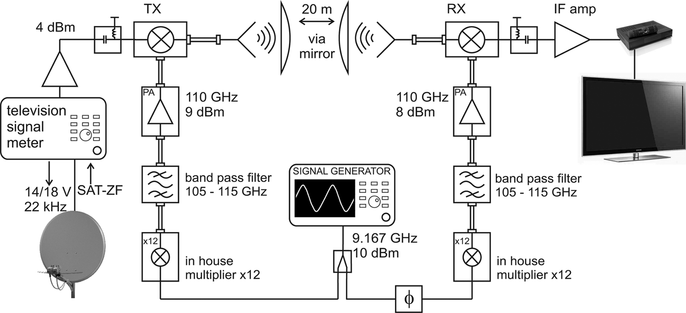
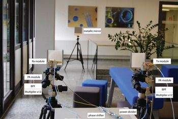
Additionally the mechanical setup for the modules has changed. Now each module as well as the mirror is mounted onto a tripod that allows rotating and tilting the modules with the attached lenses into each direction by micrometer screws. Due to this improved setup the alignment of modules and mirror is much more accurate. Figure 10 shows the setup of the 20 m link with the described LO generation components. At the lower border one can also see the tripod with the transmitter and receiver mounted as well as the HDPE lenses. In the background, the metallic mirror also mounted on a full adjustable tripod can be seen.
Photograph of a 20 m wireless data transmission. At the lower border one can see the tripod with the transmitter and receiver mounted as well as the HDPE lenses. In the background the metallic mirror also mounted on a full adjustable tripod can be seen.

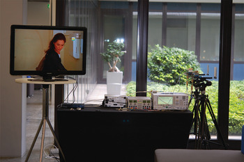
Using this new setup a data transmission of a DVS-S coded real-time television program over a distance of 20 m was performed. The television program is fetched by a satellite dish, routed via a television signal meter, amplified, and fed into the transmitter module. Normally the link between a satellite dish and a DVB-S receiver is bi-directional. The receiver gets the IF signal received by the LNB but feeds back control signals to the LNB. A 14 or 18 V DC voltage set the receiving mode to verticalor horizontal polarized reception. A 22 kHz signal switches between high or low band reception. Since the mmW wireless link is uni-directional we use a television signal meter in front of the transmitter module to set the necessary control signals manually. However, using this setup only one channel band out of four can be received. After transmitting the signal over a distance of 20 m the receiver's output signal is amplified by 23 dB and fed into a commercial DVB-S satellite receiver which is connected to a common TV. The transmission quality is sufficient for the TV to display all TV channels in one channel band in real time without errors. Figure 9 also shows the setup for the DVB-S transmission, a photograph is shown in Fig. 11.
Real-time DVB-S television transmission over a distance of 20 m. The received signal quality is sufficient for a commercial DVB-S receiver to display the television program.

V. CONCLUSION
We have demonstrated a coherent wireless data transmission using active, fully integrated MMIC modules at a carrier frequency of 220 GHz. The input sensitivity characterization of the receiver module shows an error rate of 3.0 × 10⁻⁹ for a receiver input power of −38.6 dBm and a data rate of 12.5 Gbit/s. Also the results of transmission measurements for distances of 2 and 20 m are very promising. Bit error rate measurements show performance better than 1.6 × 10⁻⁹ for 10 Gbit/s signal transmitted over 2 m. Experiments using a real-time DVB-S television signal provided via a satellite dish show that a wireless transmission over a distance of 20 m using fully integrated MMICs is feasible. The received signal quality is sufficient for a commercial DVB-S receiver to display live-TV on a television. In the future, this technology platform can provide new solutions for broadband last-mile connections and opens up a way toward a new range of wireless applications.
ACKNOWLEDGEMENTS
This work was partially carried out and funded in the frame of the Millilink project by the German Federal Ministry of Research and Education. The authors would like to thank their partners at Siemens CT and Kathrein GmbH for valuable discussions and help. Special thanks to the Institute of Photonics and Quantum Electronics, Karlsruhe Institute of Technology (KIT) for their support during the bit error rate measurements. We express our gratitude to our colleagues at IAF for their excellent contributions during epitaxial growth, wafer processing, module integration, and mechanical setup.
 Jochen Antes was born in 1983. He received the Dipl.-Ing. degree in electronic engineering from the Karlsruhe Institute of Technology, Karlsruhe, Germany, in 2010. He joined the Department of High Frequency Techniques and Electronics, Karlsruhe Institute of Technology Karlsruhe, Germany, as a research and teaching assistant, where he is currently pursuing a doctorate degree. His main interest is on high speed mixed-signal circuit design and millimeter-wave wireless links.
 Daniel Lopez-Diaz was born in 1982. He received the Dipl.-Ing. degree from the University of Karlsruhe in 2008, and is currently working toward the Ph.D. degree from the Fraunhofer Institute for Applied Solid State Physics, Freiburg, Germany. His main research interests are the design of frequency conversion circuits above 200 GHz and millimeter-wave imaging.
 Axel Tessmann received the Dipl.-Ing. and Dr.-Ing. degrees in electrical engineering from the University of Karlsruhe, Germany, in 1997 and 2006, respectively. In 1997, he joined the Fraunhofer Institute for Applied Solid State Physics, where he is involved in the development of monolithic integrated circuits and subsystems for high-resolution imaging systems up to 340 GHz. His main research areas are the design and packaging of millimeter-wave ICs using high electron mobility transistors on GaAs, GaN and InP as well as circuit simulation and linear and nonlinear device modeling. He is currently head of the millimeter-wave packaging and subsystem group at the Fraunhofer IAF.
 Arnulf Leuther received the Dipl.-Phys. degree and the Ph.D. degree in physics from the Technical University of Aachen. He has been with the Fraunhofer Institute for Applied Solid State Physics since 1996, working primarily in the development of HEMT technologies for sensor and communication systems up to 600 GHz.
 Hermann Massler was born in Radolfzell, Germany, in 1965. He studied electrical engineering at the Technical University Karlsruhe where he received the Diploma degree in 1993. While working on his diploma degree at the Kernforschungszentrum Karlsruhe (KfK) he did quasi-optical measurements at 140 GHz. He continued these studies as Research Assistant in the KfK for one more year. Since 1994, he has been with the Fraunhofer Institute for Applied Solid State Physics working on transistor and IC characterization up to 500 GHz.
 Thomas Zwick (S'95-M'00-SM'06) received the Dipl.-Ing. (M.S.E.E.) and the Dr.-Ing. (Ph.D.E.E.) degrees from the Universität Karlsruhe (TH), Germany in 1994 and 1999, respectively. From 1994 to 2001 he was research assistant at the Institut für Höchstfrequenztechnik und Elektronik (IHE) at the Universität Karlsruhe (TH), Germany. February 2001 he joined IBM as Research Staff Member at the IBM T. J. Watson Research Center in Yorktown Heights, NY, USA. From October 2004 to September 2007, T. Zwick was with Siemens AG, Lindau, Germany. During this period, he managed the RF development team for automotive radars. In October 2007, he became appointed as full professor at the Karlsruhe Institute of Technology (KIT), Germany. T. Zwick is director of the Institut für Hochfrequenztechnik und Elektronik (IHE) at the KIT. His research topics include wave propagation, stochastic channel modeling, channel measurement techniques, material measurements, microwave techniques, millimeter wave antenna design, wireless communication, and radar system design. He participated as an expert in the European COST231 Evolution of Land Mobile Radio (Including Personal) Communications and COST259 Wireless Flexible Personalized Communications. For the Carl Cranz Series for Scientific Education he served as a lecturer for Wave Propagation. He received the best paper award on the International Symposium on Spread Spectrum Techniques and Applications ISSSTA 1998. In 2005, he received the Lewis award for outstanding paper at the IEEE International Solid State Circuits Conference. Since 2008, he has been the president of the Institute for Microwaves and Antennas (IMA). T. Zwick is the author or co-author of over 100 technical papers and over 10 patents.
 Oliver Ambacher received his Dipl.-Phys. and Dr. degrees with honors from the Ludwig-Maximilians and Technical University Munich, in 1989 and 1993, respectively, where he was involved in the deposition and characterization of amorphous silicon for solar cells. In 1992, he received a German Science Foundation Graduate Research Fellowship. In 1993, he joined the Walter Schottky Institute of the TU-Munich to investigate the epitaxial growth of group-III nitrides based heterostructures. Since 1995, the research of his group is focused on fabrication of GaN–based devices like UV detectors, surface acoustic wave devices, or microwave amplifiers as well as on the understanding of polarization–induced effects in group-III nitride heterostructures and quantum wells. 1998/99, he spent one year at Cornell University, Ithaca, NY, as an Alexander von Humboldt fellow, where he was involved in the optimization of polarization–induced AlGaN/GaN HEMTs for high–frequency and high–power applications. He became a Professor of Nanotechnology and head of the Institute for Solid State Electronics located at the Technical University of Ilmenau in 2002. In 2004, he was elected as head of the new Center of Micro- and Nanotechnologies. Since 2007, he is the head of the Fraunhofer Institute of Applied Solid State Physics and Professor for Compound Microsystems in Freiburg, Germany.
 Ingmar Kallfass received the Dipl.-Ing. degree in electrical engineering from University of Stuttgart in 2000, and the Dr.-Ing. degree from University of Ulm in 2005. In 2001, he worked as a visiting researcher at the National University of Ireland, Dublin. In 2002, he joined the department of Electron Devices and Circuits of University of Ulm as a teaching and research assistant. In 2005, he joined the Fraunhofer Institute for Applied Solid State Physics with a focus on nonlinear millimeter-wave integrated circuit design. Since June 2009, he has been a professor at the Karlsruhe Institute of Technology, Karlsruhe, Germany, in the field of high–speed integrated circuits, in a shared professorship within the framework of the German Excellence Initiative.