Introduction
There is a strong environmental drive to develop alternative energy sources to coal and fossil fuels. One issue is the lack of economic impetus for some of these sources to be implemented. To harvest energy, several approaches can be taken to target different markets based on efficiency as a function of cost. In the field of photovoltaic (PV) devices for instance, crystalline silicon solar cells reach 23% efficiency in modules[Reference Green, Emery, Hishikawa, Warta and Dunlop1]; however, the sole efficiency of a PV device is to be balanced with the levelized cost of energy (LCOE). The LCOE is the ratio of the cost of an energy source over the energy produced during its lifetime, and not only includes the cost of production of the modules, but also installation and maintenance costs. As such, the LCOE is often referred to as a measure of competitiveness between various energy generation sources.[Reference Darling and You2–Reference Mulligan, Bilen, Zhou, Belcher and Dastoor4] The US Energy Information Administration presented LCOE data in its Annual Energy Outlook in 2014, and balanced the conclusions based on LCOE for electricity generation with observations based on the levelized avoided cost of electricity (LACE).[5] The report notes that the LCOE is a global tool, and tends to erase regional characteristics of a project, such as local resources and displacement of existing technologies. By comparison, the avoided cost measures the difference between the cost of electricity produced by the grid and the projected cost of electricity generated by a new energy source. The avoided cost is divided by the average annual energy output of the electricity source to yield the LACE value. By comparing the LCOE and the LACE, the project can be evaluated to estimate if the value of the project will exceed its cost (positive difference between LACE and LCOE values) and becomes economically attractive. Figure 1(a) plots the LCOE of electricity-generating plants entering service in 2019 to highlight disparities between dispatchable technologies and non-dispatchable electricity sources. The US Energy Information Administration defines dispatchable technologies as electricity sources where the energy output can be varied to follow energy demands thus creating more value, whereas non-dispatchable technologies rely on intermittent resources such as solar illumination. Based on this metric, crystalline silicon cells (utility-scale solar PV in Fig. 1) with a LCOE between 93 and 183 $/MWh may be able to directly compete with conventional coal with a LCOE between 87 and 114 $/MWh for electricity generation, in particular if coal-fired plants include carbon control and sequestration (CCS) technology increasing their LCOE to between 130 and 160 $/MWh. One observation that is striking is the LACE minus LCOE difference shown in Figs. 1(b) and 1(c), where positive values support the implementation of a studied electricity source. Figure 1(b) describes the LACE minus LCOE difference for plants entering service in 2019, and Fig. 1(c) describes the same difference for plants entering service in 2040. For plants entering service in 2019, all differences are negative (except for geothermal, which is site-specific), indicating that no new capacity is needed. Furthermore, solar PV technology becomes comparable in terms of competitiveness to coal-based electricity sources, although PV technology remains less attractive than natural gas-fired (NGF) technologies. However, with technologies becoming more mature and higher energy costs for plants entering service in 2040, solar PV is estimated to show economic advantages and could become competitive with both coal- and natural gas-based technologies.
Minimum, average, and maximum values of (a) LCOE as a function of energy-generating technology for plants entering service in 2019, and of (b) and (c) difference between LACE and LCOE estimates for plants entering service in 2019 and 2040, respectively. Legend—blue, dispatchable energy generation; green, non-dispatchable energy generation. IGCC, integrated coal–gasification combined cycle; CCS, carbon control and sequestration; NGF, natural gas-fired; CC, combined cycle; Solar PV, crystalline silicon-based devices; *, includes subsidies (adapted from[5]).

In this context favorable to solar PV, third-generation solar cells, such as copper indium gallium diselenide (CIGS) or cadmium telluride (CdTe) cells, which offer the advantage of leading to flexible, roll-to-roll processable solar devices,[Reference Reinhard, Chirila, Blosch, Pianezzi, Nishiwaki, Buechelers and Tiwari6–Reference Pethuraja, Welser and Sood8] can act as complementary technologies to silicon PV cells. In particular, solid-state organic photovoltaic (OPV) devices have the distinct advantage of being based on organic molecules or polymers with structurally tunable light absorption and electronic properties, which lead to camouflage, aesthetically pleasing,[Reference Amb, Craig, Koldemir, Subbiah, Choudhury, Gevorgyan, Jørgensen, Krebs, So and Reynolds9] or transparent devices for use in military or off-grid portable applications[Reference Krebs, Nielsen, Fyenbo, Wadstrom and Pedersen10] and in windows.[Reference Chueh, Chien, Yip, Salinas, Li, Chen, Chen, Chen and Jen11–Reference Dou, Chang, Gao, Chen, You and Yang13] The International Energy Agency highlights OPV as an emerging technology in its solar PV energy roadmap, and expects initial applications in niche, off-grid markets.[14] The roadmap further discusses the need for research efforts in the field of OPVs to focus on increasing the power-conversion efficiency (PCE) of the devices, and maintaining high efficiencies from research-scale devices to modules, as well as increasing the lifetime of OPV devices.
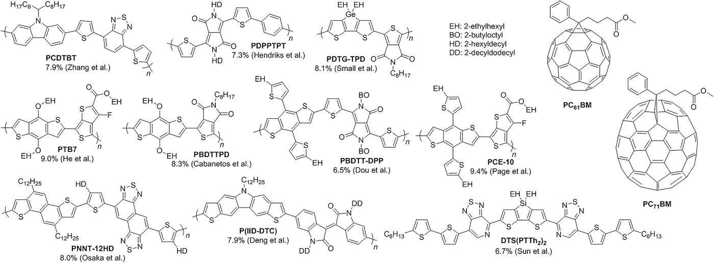
Devices prepared using OPVs provided a major breakthrough with the work of Tang who published the concept of using two different organic materials in a bilayer organic solar cell and reported a PCE of 1% in 1986,[Reference Tang15] although the idea of doping, dye mixing, multiple layering, and the need for exciton dissociation at an interface between two materials was introduced as early as 1978 by Morel et al.[Reference Morel, Ghosh, Feng, Stogryn, Purwin, Shaw and Fishman16] and Ghosh and Feng at Exxon.[Reference Ghosh and Feng17] Since then, interest has been heavy for OPVs and, although efficiencies in large-area modules still do not allow for commercial applications, significant research on new oligomer- and polymer-based materials and device engineering has led to a continuous increase in efficiencies from 1% to 12% for solid-state solar cells in both single junction and tandem architectures.[Reference Green, Emery, Hishikawa, Warta and Dunlop1, Reference Service18, 19]Fig. 2 illustrates the chemical structures for some state-of-the-art materials for OPV applications, and highlights the complexity of structure–efficiency relationships in these systems. Furthermore, PCE is greatly affected by the architecture of the OPV device, and two types of device architectures are typically used to assess the performance of novel materials: conventional and inverted architecture devices. For instance, blends of fullerene with PDTG-TPD (shown in Fig. 2) exhibits an average PCE of 7.3% in conventional devices, which increases to 8.1% in inverted devices.[Reference Amb, Chen, Graham, Subbiah, Small, So and Reynolds20, Reference Small, Chen, Subbiah, Amb, Tsang, Lai, Reynolds and So21]
Structures for a set of state-of-the-art OPV materials, with polymer and small-molecule donors and fullerene derivative acceptors.
The systems which report the highest efficiencies rely on blends of electron donating (donor) materials (small molecule or polymer) physically mixed with an electron-accepting (acceptor) fullerene derivative to form a three-phase morphological bulk heterojunction (BHJ). Conjugated polymer donors have held a strong research interest in the field of OPV due to their ease of synthesis, low-temperature solution processability, film forming ability, and mechanical integrity. As such, this Prospective will focus on polymer donors, although small molecule donors have advantages of their own, such as batch-to-batch reproducibility, and facilitated purification and characterization.[Reference Coughlin, Henson, Welch and Bazan22]
The PCE figure of merit noted earlier is the ratio of the maximum power output P max, as described in Fig. 3(a) to the input solar power. P max can be further described by the short-circuit current (J sc), open-circuit voltage (V oc), and fill factor (FF) of the device. These parameters are obtained though electrical measurements yielding current density versus voltage (J–V) curves. As mentioned previously, there is no direct correlation between molecular structure and device performance at the macroscopic level. Instead the design of π-conjugated materials is based on the feedback loop illustrated in Fig. 3(b), where the chemical structure dictates the optoelectronic properties. However, the optoelectronic properties in the solid state and phase separation of the physically mixed components are also controlled by the processing conditions. Overall, the device performance of OPVs is the result of self-assembly of polymer and fullerene into polymer-rich, fullerene-rich, and mixed domains at various length scales as discussed in the subsequent paragraph. The final morphology is controlled by molecular interactions and film drying time, and impacts photophysical and electron transfer processes involved in charge generation.
(a) Current density–voltage (J–V) and power density–voltage curves obtained under AM1.5 illustrating short-circuit current (J sc), open-circuit voltage (V oc), fill factor (FF), and the maximum power output P max. (b) Interplay between structure, material property, processing, and device performance in OPV cells.
Recent progress in understanding operating mechanisms
A major hurdle preventing an increase in the performance of OPV devices is the lack of thorough understanding of the processes involved in the formation of free charge carriers from photogenerated Frenkel excitons. Figure 4(a) illustrates the possible pathways to formation of free charge carriers upon photoexcitation of the donor material. The first step is absorption by the donor of a photon with a larger energy than the energy of the excited state of the donor (E D*) leading to excitation of the donor from the ground state (GS) to the excited state (D*) with a rate G D*. At the donor: acceptor heterojunction, electron transfer from D* to the acceptor leads to the formation of a charge transfer (CT) state with a rate k relax. This CT exciton can radiatively decay back to the GS with a rate k f or dissociate into free charge carriers in the charge separated (CS) state with a rate k CS. In the CS state, the charge carriers have overcome the Coulomb binding energy, and can find percolation pathways to their respective electrode. The binding energy of an exciton is due to the electrostatic (coulombic) attraction between the positively charged hole and negatively charged electron leading to an electron–hole pair. Organic materials tend to form excitons with binding energies around 500 meV (i.e., around 20 times thermal energy at room temperature), due to both low dielectric constant and correlation between exciton formation and geometry relaxation in π-conjugated materials.[Reference Kippelen and Bredas23] It was originally thought that charge separation required an excess of energy beyond the energy required to overcome the Coulomb attraction based on the Onsager model for ion pair separation.[Reference Askat, Adam, John, Wai-Lun, Na, Raluca, Loren, Kenrick, Kevin, Peter and Zhu24, Reference Grancini, Maiuri, Fazzi, Petrozza, Egelhaaf, Brida, Cerullo and Lanzani25] A new view relies on formation of the majority of free carriers from CT states at the donor: acceptor interface in the picosecond time scale, while excitons formed away from the interface diffuse and separate in the nanosecond time frame.[Reference Vithanage, Devižis, Abramavičius, Infahsaeng, Abramavičius, MacKenzie, Keivanidis, Yartsev, Hertel, Nelson, Sundström and Gulbinas26] Work by Gélinas et al.[Reference Gélinas, Rao, Kumar, Smith, Chin, Clark, van der Poll, Bazan and Friend27] and Vandewal et al.[Reference Vandewal, Albrecht, Hoke, Graham, Widmer, Douglas, Schubert, Mateker, Bloking, Burkhard, Sellinger, Fréchet, Amassian, Riede, McGehee, Neher and Salleo28] points to the fact that no excess energy contributed by higher energy or “hot” CT states is required for efficient charge separation.[Reference Bredas29] Rather than excess energy, delocalized band-like states are cited as being a requirement for efficient charge separation. Figure 4(b) illustrates the need for charge delocalization within fullerene aggregates at time scales of the order of a couple hundreds of femtoseconds for charge separation (yellow and red lines). By comparison, localized acceptor sites (blue line) lead to tightly bound CT states, which do not dissociate on a 100 fs time scale. This mechanism still sets emphasis not only on the energy levels of the independent donor and acceptor molecules, but also on the interactions and energy levels in mixed domains of donor and acceptor molecules. Furthermore, the optimal morphology in the BHJ needs to be rethought from pure domains of the order of tens of nanometer with mixed domains also being present to the possibility of films made up of mostly mixed domains with smaller pure domains as percolation pathways.
Processes involved in charge separation: (a) absorption from the ground state (GS) to the donor excited state (D*) followed by either direct charge separation with a rate of k*CS or relaxation to the lowest energy charge transfer state (CT1) then charge separation; (b) driving force for charge separation through charge delocalization into large fullerene aggregates (yellow and red) and hindered charge separation in the absence of delocalization (blue) (adapted from[Reference Gélinas, Rao, Kumar, Smith, Chin, Clark, van der Poll, Bazan and Friend27, Reference Vandewal, Albrecht, Hoke, Graham, Widmer, Douglas, Schubert, Mateker, Bloking, Burkhard, Sellinger, Fréchet, Amassian, Riede, McGehee, Neher and Salleo28]).
The first optical transition occurs from the GS to the excited state of the polymer donor for instance, and can be approximated by the transition from the highest occupied molecular orbital (HOMO) of the polymer and its lowest unoccupied molecular orbital (LUMO), which ties into the geometric difference between the aromatic and quinoidal structures. To tune the energy gap E D* illustrated in Fig. 4(a), the alternating donor–acceptor (D–A) approach shown in Fig. 5 is commonly used and relies on the fact that the HOMO of the donor moiety and the LUMO of the acceptor moiety largely dictate the HOMO and LUMO in the resulting D–A alternating structure. The strength of the D–A concept resides in the ease of control over frontier energy levels and energy gap, along with the endless library of electron-rich and electron-poor conjugated units, which can be employed in materials design and synthesis.[Reference Li, You, Müllen, Reynolds and Masuda30] The π-conjugated polymer backbone is typically functionalized by alkyl side-chains to induce solubility into these generally rigid polymers, although other side-chain functionalities can be selected as part of the polymer design.[Reference Mei and Bao31]
Donor–acceptor design and representative electron-rich donor and electron-deficient acceptor units to tune the energy of frontier molecular orbitals in conjugated materials (adapted from[Reference Li, You, Müllen, Reynolds and Masuda30]).
Electron-rich units are typically based on thiophene, furan, and pyrrole rings, which can be further fused with other aromatic rings to increase the rigidity of the polymer backbone. For instance, dioxythiophenes have increased electron-richness compared with thiophenes due to the electron-donating oxygens on the thiophene ring and provide a handle for functionalization away from the polymer backbone, which can prevent twisting and may lead to increased interchain interactions. Electron-deficient units are typically based on imine-like nitrogen-containing heterocyclic rings (e.g., triazole and thiadiazole)[Reference Li, You, Müllen, Reynolds and Masuda30, Reference Parker, Patel, Moudgil, Barlow, Risko, Bredas, Reynolds and Marder32] or other aromatic rings with amide or imide functionalities,[Reference Robb, Ku, Brunetti and Hawker33–Reference Guo, Facchetti and Marks35] or fluorine substitution[Reference Zhou, Yang, Stuart, Price, Liu and You36, Reference Son, Wang, Xu, Liang, Wu, Li and Yu37] as π- or σ- electron-withdrawing groups, respectively. Material design of D–A polymers hence needs to take into account aromaticity and bond length alternation, rigidity, and planarity of the polymer backbone, side-chain functionalization, and interchain interactions. In particular, the rigidity of the polymer backbone can be used to maximize π-conjugation and reduce the energy gap by constructing ladder-type polymers.[Reference Scherf, Skotheim, Elsenbaumer and Reynolds38, Reference Babel and Jenekhe39] The D–A concept has led to the synthesis of a conjugated polymer with an optical energy gap as low as 0.5 V by alternating a strong donor dithieno[3,2-b:2′,3′-d]pyrrole with a strong acceptor benzo[1,2-c;4,5-c′]bis[Reference Green, Emery, Hishikawa, Warta and Dunlop1, Reference Darling and You2, 5]thiadiazole.[Reference Steckler, Zhang, Hwang, Honeyager, Ohira, Zhang, Grant, Ellinger, Odom, Sweat, Tanner, Rinzler, Barlow, Brédas, Kippelen, Marder and Reynolds:40] For an early, thorough review of energy gap engineering via D–A concepts, the reader is directed to the work of van Mullekom et al.[Reference van Mullekom, Vekemans, Havinga and Meijer41]
Impact of material design and processing on morphology
Beyond the molecular formula, the resulting material properties are also based on interactions in the solid state, which makes molecular design a challenging task. The device performance and properties at the macroscopic level are due to structural effects over a range of length scales, extending from molecular packing at the angstrom and nanometer scale to phase separation at the microscopic scale as shown in Fig. 6. Indeed, van der Waals, dipolar and hydrogen-bonding interactions at the angstrom scale will dictate molecular packing, which in turn will control molecular ordering at the nanoscale. In the case of polymer: fullerene blends, the formation of a three-phase morphology containing polymer crystallites, fullerene aggregates, and mixed regions of amorphous polymer chains with incorporated fullerene molecules is crucial to device performance.[Reference Burke and McGehee42, Reference Sweetnam, Graham, Ngongang Ndjawa, Heumüller, Bartelt, Burke, Li, You, Amassian and McGehee43] At the device scale, polymer- and fullerene-rich domains can be visualized using techniques such as transmission electron microscopy and atomic force microscopy. Overall, the morphology over the various length scales is a result of both thermodynamic (material interactions) and kinetic (film drying time: solvent vapor pressure, deposition conditions) parameters, as most of the conditions used for solution processing lead to metastable morphologies due to the relatively fast drying times (10–300 s depending on the solvent system and processing method).[Reference Richter, DeLongchamp, Bokel, Engmann, Chou, Amassian, Schaible and Hexemer44, Reference Abdelsamie, Zhao, Niazi, Chou and Amassian45]
Morphological considerations in the active layer of OPVs, ranging from the molecular scale to the micrometer scale (adapted from[Reference Rivnay, Mannsfeld, Miller, Salleo and Toney46]).
At the molecular level, the degree of ordering in these semi-crystalline polymers will depend on several parameters: molecular weight,[Reference Kline47] steric arrangement of the side-chain,[Reference Guilbert, Frost, Agostinelli, Pires, Lilliu, Macdonald and Nelson48] nature of the polymer backbone, branching and defects, chain ends,[Reference Park, Jo, Seo, Moon, Park, Lee, Heeger and Bazan49] and interchain interactions, in addition to factors controlled by processing (polymer solubility, film drying time, etc.).[Reference Kouijzer, Michels, van den Berg, Gevaerts, Turbiez, Wienk and Janssen50] Interchain interactions in polymers based on dithienocyclopentadiene- and dithienosilole-benzodiathiazole (CPDT-BTD and DTS-BTD, respectively) have been studied both experimentally and computationally. As summarized in Fig. 7(a), solid-state NMR results demonstrate that the repeat units are π-stacked, and showed that the BTD acceptor units are heterogeneously packed throughout the sample (the acceptor groups are not always located at the exact same position with respect to the neighboring polymer chains).[Reference Beaujuge, Tsao, Hansen, Amb, Risko, Subbiah, Choudhury, Mavrinskiy, Pisula, Brédas, So, Müllen and Reynolds51, Reference Wang, Kappl, Liebewirth, Müller, Kirchhoff, Pisula and Müllen52] These solid-state NMR results are supported by molecular modeling where donor-on-donor/acceptor-on-acceptor stacking with a small shift along the polymer backbone was determined to be the most likely intermolecular packing geometry.[Reference Guilbert, Frost, Agostinelli, Pires, Lilliu, Macdonald and Nelson48] In the case of copolymers composed of fused dithienyl units and BTD units, it appears that the flipped stacking dictates interchain interactions. Another model for molecular packing is the “molecular docking” scheme, where smaller electron-rich units, for instance, are stacked over larger electron-deficient units as discussed by Lei et al.[Reference Lei, Cao, Zhou, Peng, Bian and Pei53] in the case of isoindigo-containing polymers. Furthermore, the interactions between polymer donor and fullerene acceptor [Fig. 7(b)] have been highlighted as a crucial component to the generation of an energy landscape favorable to CT and separation.[Reference Graham, Cabanetos, Jahnke, Idso, El Labban, Ngongang Ndjawa, Heumueller, Vandewal, Salleo, Chmelka, Amassian, Beaujuge and McGehee54] Both interactions lead to important trends in material design to achieve control over the CT states and phase separation.
Intermolecular interactions between (a) polymer chains and (b) at the polymer: fullerene heterojunction (adapted from[Reference Graham, Cabanetos, Jahnke, Idso, El Labban, Ngongang Ndjawa, Heumueller, Vandewal, Salleo, Chmelka, Amassian, Beaujuge and McGehee54, Reference Tsao, Cho, Park, Hansen, Mavrinskiy, Yoon, Graf, Pisula, Spiess and Müllen55]).
At the microscopic level, physical mixing of the two components in solution followed by solution processing allows for little control over the final phase separation. However, several processing parameters can be tuned to reach an optimized morphology in the active layer for enhanced device performance. The development of novel in situ characterization techniques of thin films as they dry has shed some light on film formation mechanisms.[Reference Richter, DeLongchamp, Bokel, Engmann, Chou, Amassian, Schaible and Hexemer44, Reference Shin, Richter, Herzing, Kline and DeLongchamp56–Reference Chou, Yan, Li, Li, Zhao, Anjum, Alvarez, Gassaway, Biocca, Thoroddsen, Hexemer and Amassian58] A first challenge is determining the mechanisms that drive phase separation during solution deposition. Kouijzer et al.[Reference Kouijzer, Michels, van den Berg, Gevaerts, Turbiez, Wienk and Janssen50] have described a ternary phase diagram made up of solvent, polymer, and fullerene derivative, and have divided the mechanism for phase separation into three main categories: liquid–liquid demixing, liquid–solid demixing, or no phase separation. As illustrated in Fig. 8, the contribution of each category depends on the kinetics of film formation (quenching of liquid–liquid demixing relative to allowing for aggregates to form and grow) and on the structure of the compounds (interactions that have the possibility to lead to aggregation compared with steric bulk that decreases that probability). The process shown to the left of Fig. 8 illustrates the liquid–liquid pathway to phase separation, which is typically followed in blends cast from chloroform due to the fast drying time that prevents aggregation of either two components. Other single solvent systems, based on chlorobenzene or o-dichlorobenzene (oDCB) for instance, will follow liquid–liquid demixing if liquid–solid demixing is not favored (polymer self-assembly is sterically hindered for instance) or if the film drying time does not allow for aggregation of the polymer or fullerene. The two drying mechanism to the right of Fig. 8 illustrate the presence of polymer (center) or fullerene (right) aggregates either in the casting solution or in the drying film, and how this solid–liquid demixing controls the phase separation in these blends. In the case of solid–liquid demixing, polymer crystallization or fullerene aggregation dictates the phase separation in the active layer, with the fullerene molecules mixed into the amorphous domains of the polymer in one case and the polymer chains aggregating around the fullerene aggregates in another.
Scheme summarizing various processes that can occur during film formation in BHJ devices. Solvent molecules: white circles; polymer chains: blue lines (polymer crystallites: rod-like, amorphous polymer: random-like chains); fullerene molecules: brown circles (adapted from[Reference Kouijzer, Michels, van den Berg, Gevaerts, Turbiez, Wienk and Janssen50]).
Addition of a high boiling point additive to the casting solution has been shown to have a drastic impact on phase separation in polymer: fullerene blends.[Reference Peet, Kim, Coates, Ma, Moses, Heeger and Bazan59–Reference Yao, Hou, Xu, Li and Yang62] The method of using a main solvent with a high vapor pressure for fast evaporation, leaving behind a lower vapor pressure “tailing” solvent to further shape the thin-film morphology has been extensively used in the coating industry. In the field of OPV, Peet et al.[Reference Peet, Kim, Coates, Ma, Moses, Heeger and Bazan59] introduced octanedithiol (ODT) as a solvent additive and showed increased OPV device performance. Since then, research efforts have focused on understanding the mechanisms involved in morphology control when solvent additives are used. As of today, it appears that the aliphatic versus aromatic structure of the additive is the main factor behind the differences in thin-film formation. This is linked to the fact that the thin-film morphology is set in two stages: at the solution stage with pre-aggregation and at the drying stage, which has been shown to last over 40 min in some cases.[Reference Rogers, Schmidt, Toney, Bazan and Kramer63] In particular, solvent additives can be separated into two categories: good solvent for both polymer and fullerene (typically aromatic additives), or poor solvent for polymer chains and good solvent for fullerene derivatives (typically aliphatic additives).
Using grazing-incidence small-angle x-ray scattering on solutions with and without solvent additive, Schmidt et al.[Reference Schmidt, Tassone, Niskala, Yiu, Lee, Weiss, Wang, Fréchet, Beaujuge and Toney64] and Lou et al.[Reference Lou, Szarko, Xu, Yu, Marks and Chen65] point out differences in the behavior of polymers and fullerene derivatives in solution. Schmidt et al.[Reference Schmidt, Tassone, Niskala, Yiu, Lee, Weiss, Wang, Fréchet, Beaujuge and Toney64] show that diketopyrrolopyrole-based polymer chains in chlorobenzene are aggregated and that addition of 5%vol. 1-chloronaphthalene (CN) in the solution induces more ordered aggregates (presence of a swelled lamellar-type peak). The hypothesis is that CN leads to ordered aggregates that then act as nucleating sites for polymer ordering. Increasing the number of nucleating sites for the polymer lamella decreases the size of polymer-rich domains. On the other hand, work by Lou et al.[Reference Lou, Szarko, Xu, Yu, Marks and Chen65] indicates that fullerene aggregates in chlorobenzene decrease in size when 1,8-diiodooctane (DIO) is added to the solution, leading to increased miscibility between the polymer and fullerene domains, with smaller domain sizes overall. Bridging these two studies, research by Shin et al.,[Reference Shin, Richter, Herzing, Kline and DeLongchamp56] Richter et al.,[Reference Richter, DeLongchamp, Bokel, Engmann, Chou, Amassian, Schaible and Hexemer44] and Gao et al.[Reference Gao, Chen, Dou, Chen, Chang, Liu, Li and Yang66] has compared effects stemming from aliphatic and aromatic additives in blade-coated or spun cast blends. In blends of poly(3-hexylthiophene) (P3HT) with PC61BM blade-coated from a chlorobenzene solution, P3HT crystals are formed as chlorobenzene evaporates. Addition of CN to a chlorobenzene solution leads to an increased growth of P3HT crystals from a CN solution of P3HT and PC61BM, as well as solid P3HT crystallites formed after chlorobenzene evaporation. On the other hand, addition of ODT to the chlorobenzene solution leads to the formation a three phase system containing solid P3HT crystallites, a liquid phase of PC61BM and a mixed liquid phase of P3HT and PC61BM, resulting in a slight increase in the growth of P3HT crystals as ODT evaporates. In the case of P3HT, the authors demonstrate that solvent additives can be viewed as plasticizers for the P3HT chains either through swelling of the polymer-rich domains to enable further chain motion or by selectively removing fullerene molecules from polymer-rich phases.[Reference Shin, Richter, Herzing, Kline and DeLongchamp56] In PBDTP-DPP:PC71BM blends, Gao et al.[Reference Gao, Chen, Dou, Chen, Chang, Liu, Li and Yang66] observed negligible shift in the absorption maximum of the polymer solution with 1%vol. DIO and a 11 nm red-shift when 3%vol.oDCB is added. The authors thus concluded that addition of DIO to a polymer solution in chloroform leads to the formation of amorphous aggregates in the chloroform solution, whereas addition of oDCB forms more ordered aggregates, on par with the findings of Schmidt et al.[Reference Schmidt, Tassone, Niskala, Yiu, Lee, Weiss, Wang, Fréchet, Beaujuge and Toney64] with CN as an aromatic additive. Overall, both mechanisms depend on the self-assembly of fullerene aggregates and polymer chains,[Reference Yan, Zhu, Li, Zhang, Yi, Yang, Wei and Brédas67] and lead to solid–liquid demixing and increased PCEs in OPV devices. The impact of processing additives on the morphology of BHJ films in general drives research toward an in depth understanding of the factors impacting phase separation, and will allow for faster development of large-area BHJ devices.
Challenges in moving toward modules
From a material standpoint, reproducibility of the device results is a limiting factor in achieving repeatable efficiencies in larger-scale OPV modules. Indeed, P3HT has been reported to have maximum PCEs ranging from about 1.5% to 4.5% (Fig. 9) depending on the batch of polymer and device fabrication conditions.[Reference Dang, Hirsch and Wantz68] The batch-to-batch variation in polymer synthesis is one of the hardest issues to tackle. A first issue is the limited molecular weight estimations, which can be obtained by size exclusion chromatography (SEC) using THF as an eluent and polystyrene as a standard. However, THF is a poor solvent for some conjugated polymers, and polystyrene has a different conformation than conjugated polymers. Some alternatives are being explored, such as the use of high-temperature SEC and/or the use of 1,2,4-trichlorobenzene as the eluent. Furthermore, π-conjugated polymers synthesized by step-growth cross-coupling reactions tend to have broad dispersities (around or above 2.0) leading to materials that are not precisely defined as would be the case for small molecules. The fact that these are high molecular weight systems also limits the accurate determination of chemical structure, material purity, and nature of the end-groups on the polymer chains.[Reference Park, Jo, Seo, Moon, Park, Lee, Heeger and Bazan49] The study conducted by Hendriks et al.[Reference Hendriks, Li, Heintges, van Pruissen, Wienk and Janssen69] is of particular relevance as the authors demonstrate the presence of homocoupling defects along a polymer chain depending on the polymerization conditions, which lead to a decrease in PCE from 7.5% to 4.5–5.6%. As such, polymer chemistry remains a central part of the development of OPV technology.
(a) Power-conversion efficiencies of the P3HT:PC61BM-based solar cells. Each dot corresponds to the maximum PCE value reported in each publication. (b) The overall distribution of PCE values from 2002 to 2010 (reprinted from[Reference Dang, Hirsch and Wantz68]).
Beyond material synthesis and characterization, Zimmermann et al.[Reference Zimmermann, Ehrenreich, Pfadler, Dorman, Weickert and Schmidt-Mende70] and Luber and Buriak[Reference Luber and Buriak71] have insisted on the need for standardized testing of OPV devices beyond the AM1.5 standard illumination, through the use of shadow masks for instance, and the need to determine whether the reported findings are statistically relevant.
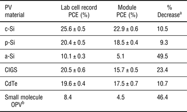
The choice of processing technique at an industrial scale is also crucial in terms of technology development for organic electronic in general, and OPVs in particular, as it will define the efficiency, throughput, and thus the cost of devices manufactured on an industrial scale. As highlighted in Table I, a challenge in the field of OPVs is to bridge the gap between efficiencies reached at the laboratory scale and over larger areas in modules. Currently, OPVs suffer a large drop in efficiency (close to 47% for a small molecule-based OPV device developed by imec and Solvay,[106] which is comparable to the drop in efficiency observed in amorphous silicon (a-Si) devices) as defined in Table I in transitioning from laboratory-scale devices to large-area modules. By comparison, monocrystalline silicon (c-Si), polycrystalline silicon (p-Si), or CdTe cells only exhibit a drop in efficiency from 20% or more PCE in research-scale cells to 15% or more in modules. If OPV modules only showed a 20% loss in PCE compared with research-scale devices (instead of 47% for instance), modules with PCE of 8.5% could be manufactured, which would set OPV efficiencies in modules above the 5% efficiencies found in a-Si modules.
Decrease in PCE going from research PV cells to modules (adapted from[Reference Green, Emery, Hishikawa, Warta and Dunlop1, Reference Darling and You2, 106]).
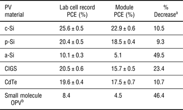
a % Decrease = (Lab PCE − Module PCE)/Lab PCE.
b Imec and Solvay: fullerene-free device based on evaporated small molecule active layers.
Historically, the goal for solution-processed organic electronic devices was for roll-to-roll, continuous manufacturing using shearing processes, such as slot-die coating.[Reference Krebs, Gevorgyan and Alstrup72, Reference Machui, Lucera, Spyropoulos, Cordero, Ali, Kubis, Ameri, Voigt and Brabec73] Other continuous printing processes include spray-coating and inkjet printing.[Reference Teichler, Eckardt, Hoeppener, Friebe, Perelaer, Senes, Morana, Brabec and Schubert74] On the research scale, efforts are focused on spin coating as the processing method for the active layer in organic electronics. While spin coating provides thin films, there can be morphological disparities across small distances, and it is not amenable to continuous processing; thus 90% of the coating solution is wasted.[Reference Arias, MacKenzie, McCulloch, Rivnay and Salleo75] Furthermore, even at the research scale, large-area spin coating presents technological challenges.[Reference Jin, Tao, Velusamy, Aljada, Zhang, Hambsch, Burn and Meredith76] For these reasons, the drive is now to translate the guidelines established using spin coating to other processing techniques,[Reference Xiong, Hou, Wu, Huo, Mo, Yuan, Sun, Xu and Wang77] which could also provide control of polymer chain alignment to promote crystalline regions, reduce grain boundaries between neighboring crystalline domains, and dictate orientation alignment[Reference Giri, Verploegen, Mannsfeld, Atahan-Evrenk, Kim, Lee, Becerril, Aspuru-Guzik, Toney and Bao78] and improve intermolecular orbital overlap.[Reference Yao, Dong and Hu79] Blade coating stands out as a processing technique bridging laboratory-scale devices and roll-to-roll manufacturing.[Reference Shin, Richter, Herzing, Kline and DeLongchamp56, Reference Lim, Chen, Chen, Ong, Chen and Meng80] Ultimately, slot-die coating appears as the targeted solution-processing technique as it provide continuous processing with little material waste and control of the film homogeneity.[Reference Amb, Craig, Koldemir, Subbiah, Choudhury, Gevorgyan, Jørgensen, Krebs, So and Reynolds9, Reference Søndergaard, Manceau, Jørgensen and Krebs81] Other types of solution processing techniques include spray deposition,[Reference Abdellah, Virdi, Meier, Döblinger, Müller-Buschbaum, Scheu, Lugli and Scarpa82] and inkjet printing.[Reference Teichler, Eckardt, Hoeppener, Friebe, Perelaer, Senes, Morana, Brabec and Schubert74] The main advantage of inkjet printing is the capability for patterning with micrometer resolution, which makes it ideal for screening device fabrication conditions. However, the resulting films have low thickness uniformity and solvent evaporation may clog the nozzle, which limits the solvent options accessible for this technique. Furthermore, compared with vacuum deposition or physical vapor deposition of small molecule thin films, solution-based processing also presents challenges for multiple layer deposition, which can be solved by using orthogonal solvents or by solubility modification of the underlying layer.[Reference Patel, Graham and Reynolds83] Encouragingly, the groups of Krebs and Brabec have developed materials and processes for fabrication of tandem architecture compatible with roll-to-roll manufacturing.[Reference Li, Kubis, Forberich, Ameri, Krebs and Brabec84–Reference Spyropoulos, Kubis, Li, Baran, Lucera, Salvador, Ameri, Voigt, Krebs and Brabec86] By combining an efficient recombination layer that does not require thermal annealing and using blade-coating to sequentially deposit the layers involved in the tandem device, the authors reached average PCEs of 7.5% and 5.3% on glass substrates and flexible PET substrates, respectively. This work demonstrates direct applicability of OPV technology to roll-to-roll processes to reach higher efficiencies enabled by devices with tandem architectures.
Outlook
Significant research efforts focus on designing new donor materials to reach high efficiencies.[Reference Andersen, Dam, Hosel, Helgesen, Carle, Larsen-Olsen, Gevorgyan, Andreasen, Adams, Li, Machui, Spyropoulos, Ameri, Lemaitre, Legros, Scheel, Gaiser, Kreul, Berny, Lozman, Nordman, Valimaki, Vilkman, Sondergaard, Jorgensen, Brabec and Krebs85] However, the recent model for charge separation in OPVs can also lead to opportunities in discovering alternatives to fullerene derivatives to achieve complementary light absorption between donor and acceptor materials. There are at least two areas of interest for the use of non-fullerene acceptors. One is the development of universal acceptors, which could be used with different donor materials.[Reference Lin and Zhan87] One example is a decacyclene triimide-based small molecule with a three-dimensional (3D) structure imparted by the steric hinderance from the outer phenyl rings, which yields efficiencies over 1% with a wide range of polymer donors,[Reference Pho, Toma, Tremolet de Villers, Wang, Treat, Eisenmenger, Su, Coffin, Douglas, Fréchet, Bazan, Wudl and Chabinyc88] and its universality can be in part explained by the availability of electron accepting states in this acceptor, which is comparable with what is calculated for fullerene derivatives.[Reference Liu and Troisi89] The concept of using 3D acceptors has also been reported by Li et al.,[Reference Li, Earmme, Ren, Saeki, Yoshikawa, Murari, Subramaniyan, Crane, Seki and Jenekhe90] where two planar 7,9,16,18-tetraazabenzodifluoranthene-3,4,12,13-tetracarboxylic acid diimide units are linked through a thiophene ring to create a twisted 3D acceptor (DBFI-T) leading to an improvement in the PCE of PSEHTT: acceptor cells from 3.5% with PC61BM to 4.2% with DBFI-T. The second opportunity is understanding the less efficient charge separation in blends with non-fullerene acceptors compared with blends with fullerenes[Reference Bloking, Giovenzana, Higgs, Ponec, Hoke, Vandewal, Ko, Bao, Sellinger and McGehee91] as studied by Bakulin et al.[Reference Bakulin, Rao, Pavelyev, van Loosdrecht, Pshenichnikov, Niedzialek, Cornil, Beljonne and Friend92] and illustrated in Fig. 10(a). For instance when polymer-based electron acceptors are used, the charge distribution (quantified by the average distance between hole and electron, R) is more localized in the case of polymer: polymer heterojunctions than in polymer: fullerene heterojunctions, which is one possible explanation for the lower PCEs achieved in all-polymer blends.
(a) Microelectrostatic simulations of the charge distribution in the CT state at the P3HT:PF8BT heterojunction, with electron and hole densities shown in blue and red, respectively. (b) Donor and acceptor polymers in state-of-the-art all-polymer active layer (adapted from[Reference Bakulin, Rao, Pavelyev, van Loosdrecht, Pshenichnikov, Niedzialek, Cornil, Beljonne and Friend92, Reference Earmme, Hwang, Murari, Subramaniyan and Jenekhe93]).
One opportunity for the design of new electron accepting materials and for morphology control is the use of polymer: polymer blends and block copolymers. In the case of all-polymer blends, Mori et al.[Reference Mori, Benten, Ohkita, Ito and Miyake94] have achieved PCEs of 2.6% on average in blends of P3HT and poly[2,7-(9,9-didodecylfluorene)-alt-5,5-(4′,7′-bis(2-thienyl)-2′,1′,3′-benzothiadiazole)] (PF12TBT) thanks to a large V oc of 1.3 V; however, the J sc and FF remain low at 3.9 mA/cm2 and 55%, respectively. Increased charge-carrier transport thanks to increased molecular weight of the acceptor polymer and thermal annealing is cited as the rationale for the high PCE; however, no measure of mobility is given in the study. Earmme et al.[Reference Earmme, Hwang, Murari, Subramaniyan and Jenekhe93] have reported a 3.2% average PCE in PSEHTT:PNDIS-HD blends (equal to the PCE of PSEHTT:PC61BM, mostly thanks to a V oc of 0.75 V compared with 0.64 V in the case of blends with PC61BM). This high efficiency for all-polymer BHJ devices was rationalized by balanced charge-carrier transport of the order of 10−4 cm2V−1s−1 for both hole carrier and electron carrier mobility measured through the blend using space-charge limited current measurements. In this case, however, the phase separation was of the order of 200 nm but did not hinder charge generation. Further work on this system investigated reducing the phase separation by spin coating the blend of two polymers from a chlorobenzene:oDCB (90:10) mixture, leading to a reduction in the phase separation from over hundreds of nanometers to tens of nanometers and an increase in PCE to 4.7%.[Reference Earmme, Hwang, Subramaniyan and Jenekhe95] A similar NDI-based polymer acceptor, PC-NDI, was studied in blends with P3HT, PTB7, and TTV7 by Zhou et al.[Reference Zhou, Cong, Hashimoto and Tajima96] In this study, it was hypothesized that TTV7 exhibits the highest miscibility with PC-NDI, and that addition of DIO leads to an increase in the crystallinity of PC-NDI and a balanced hole and electron carrier mobility in the BHJ blend. This balanced charge-carrier mobility again seems to be linked to high PCE in all-polymer blends, with the average efficiency in TTV7:PC-NDI blends measured at 3.6%. As such, the design of acceptor polymers with high-energy excited states (i.e., low electron affinity) to increase V oc, while still enabling efficient charge separation, and with high electron carrier mobility through the bulk should be targeted, with the possibility of tuning phase separation by promoting polymer mixing through favorable polymer: polymer interactions[Reference Li, Roelofs, Turbiez, Wienk and Janssen97] or unfavorable polymer: solvent interactions.[Reference Pavlopoulou, Kim, Lee, Chen, Facchetti, Toney and Loo98] Block copolymers containing donor and acceptor fractions also appear to be an elegant way to control phase separation, and have been discussed in a review by Robb et al.[Reference Robb, Ku and Hawker99]
Device engineering also holds vast opportunities for growth, in particular in terms of PV device stability. For instance, compared with conventional devices, inverted devices have the advantage of employing high work-function cathode materials as the top layer, which can be both solution-processed and are not sensitive to oxidization in air. These two factors, solution- processability and air stability, make inverted devices amenable to roll-to-roll processing at the module level.[Reference Lucera, Kubis, Fecher, Bronnbauer, Turbiez, Forberich, Ameri, Egelhaaf and Brabec100] Studies revealed that, over time, most of the failures in OPV devices stem from interfacial degradation at the interface between the active layer and PEDOT:PSS for instance,[Reference Angmo, Sommeling, Gupta, Hösel, Gevorgyan, Kroon, Kulkarni and Krebs101] and from phase separation that is unstable to temperatures above the glass transition temperature of the polymer in the BHJ.[Reference Sachs-Quintana, Heumüller, Mateker, Orozco, Cheacharoen, Sweetnam, Brabec and McGehee102] These observations yield further insight into the behavior of OPV devices during their lifetime, and trigger new opportunities for material research such as highly conductive, solution processable electrode materials[Reference Vosgueritchian, Lipomi and Bao103, Reference Puodziukynaite, Wang, Lawrence, Wise, Russell, Barnes and Emrick104] or conjugated polymers with high glass transition temperatures.
In conclusion, there is no doubt that there is room for growth for OPV devices, in particular considering the processing and efficiency gap between research-scale devices and large-area modules. Particularly encouraging results include slot-die coated 1 inch-squared OPV cells on flexible substrates using non-halogenated solution formulations,[Reference Machui, Lucera, Spyropoulos, Cordero, Ali, Kubis, Ameri, Voigt and Brabec73] and the development of a 3% PCE all-plastic OPV device.[Reference Zhou, Fuentes-Hernandez, Shim, Meyer, Giordano, Li, Winget, Papadopoulos, Cheun, Kim, Fenoll, Dindar, Haske, Najafabadi, Khan, Sojoudi, Barlow, Graham, Brédas, Marder, Kahn and Kippelen105] Furthermore, imec and Solvay were able to develop 160 cm2 modules with 5% PCE in devices processed by thermally evaporating small molecules and 4.5% PCE in polymer: fullerene blends. The engineering of both small molecule and polymer: fullerene blend-based devices was optimized to increase the stability and lifetime of the devices.[106] The combined efforts in material development and device engineering will surely drive OPV devices to reach their potential in solar modules.
Acknowledgments
This publication is based on the work supported in part by Grant No. N00014-14-1-0173 from the Office of Naval Research. The authors thank Dr. Bernard Kippelen for helpful discussions during the writing of this manuscript.