I. INTRODUCTION
Diamond films are regarded as a kind of ideal material for cutting tool films in modern industry for its unique characteristics, such as high hardness, high equivalent elastic modulus, good thermal conductivity, good chemical durability, low friction and thermal expansion coefficient, high corrosion resistance, and so on. Reference Liu, Bian, Zheng, Zhu, Chen, Chen and Wang1–Reference Straffelini, Scardi, Molinari and Polini3 Many experiments and operations reveal that the diamond films can improve service life of cutting tools and machining precision effectively. Reference Zhang, Shen and Sun4 So the diamond films are always used for processing intractable materials, such as superhard material, nonferrous metal, nonmetallic material, composite material etc., which make them credit for extensive using. Reference Nibennaoune, Geprge, Ahzi, Ruch, Remond and Gracio5 People have made much development and achievements on depositing the diamond films by now, there are mainly two ways, i.e., physical vaporous deposition Reference Pigeat, Miska, Bougdira and Easwarakhanthan6 and chemical vaporous deposition (CVD). Reference Zhu, Miao, Liu, Chen, Guo, Hua, Ding, Lian and Li7,Reference Younes, Jacky, Didier and Miche8 CVD has great application prospect in surface modification treatment of cemented carbides, Reference Shen, Sun, Zhang, Shen and Guo9 which is suitable for the substrates with all shapes. Therefore, the diamond film is always considered to improve service life of cutting tools and machining quality. Reference Jansen, Dorsch, Obermeier and Kulisch10 In the past decades, CVD technology has made great effect on the development of industry. Reference Tang, Fernandes, Jiang, Pinto and Ye11,Reference Wei, Yu, Michael, Ashfold and Ma12 In this study, the surface-interface morphologies and compositions of chemical elements of diamond films on YT14 cemented carbide cutting tools were investigated with a scanning electron microscopy (SEM), and its configured energy dispersive spectrometer, respectively. The phases, atomic bonding energies, and structures of the film were determined with an x-ray diffraction (XRD), x-ray photoelectron spectroscopy (XPS), and Raman, respectively, and the surface roughness was analyzed by atomic force microscopy (AFM). Nano indenter was the measurement tool to evaluate the mechanical properties, and the bonding strength of the films was evaluated by a scratch tester.
II. EXPERIMENTAL
YT14 cemented carbide cutting tools were chose as a substrate with the chemical compositions as follows (mass%): WC 78, TiC 14, and Co 8, and the size of substrate was 16 mm × 16 mm × 5 mm. The samples were cleaned in alcohol to remove oil and dust and rinsed in deionized water and baked in a heater. Then, the samples were put into a CVD deposition system with the hot filament of tantalum wire, the distance between the hot filament and substrate was 5 mm, and the bias current was 0.15–0.3 A/cm2. The process of CVD was shown as follows: carbon source gas with methyl (–CH3) (corresponding to 0.5–10 vol%), including methane (CH4), acetone (CH3COCH3), and hydrogen (H) were bubbled into a vacuum deposition chamber. The huge of methyl (–CH3) interacted with each other at high temperature of 2100–2200 °C and low pressure of 2–8 kPa, then the carbon (C) would link with each other via covalent bonds. As the deposition continues, the diamond nucleation was formed on the substrate at 800–850 °C, the protium (1H) in the nucleation was replaced by –CH3. After 2 h, the diamond film was achieved. Reference Morales, Apátiga and Castaño13 The surface-interface morphologies, chemical compositions, and phases of the diamond film were analyzed with a JSM-6360LA type SEM (JEOL Ltd., Tokyo, Japan), electronic energy spectrum (EDS), and D/max 2500PC type XRD (Rigaku Corporation, Tokyo, Japan), respectively. The bonding spectra of chemical elements was observed on a thermo ESCALAB 250 type of XPS (Thermo Fisher Scientific, Waltham, Massachusetts) with excitation source of X-ray, the measurement parameters as follows: monochromatic target of Al Kα (hν = 1486.6 eV), power of 150 W, x-ray beam spot of 500 μm, and fixed energy of energy analyzer: 30 eV. The surface roughness was measured with a CSPM5500 type atomic force microscope (AFM; Being Nano-Instrument Ltd., Beijing, China). The indentation was analyzed with a nanomechanical testing system with a Berkovich needle (curvature radius was 50 nm; Hysitron, Minneapolis, Minnesota). The bonding strength was measured with a WS-2005 type film adhesion tester (Lanzhou Institute of Chemistry Physics, Lanzhou, China), the test way was acoustic emission (AE), and the measurement parameters: load of 100 N, loading rate of 50 N/min, scratch length of 4 mm.
III. ANALYSIS AND DISCUSSION
A. Surface morphology and EDS analysis
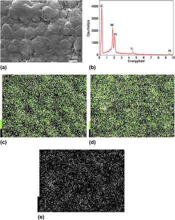
Figure 1(a) shows the surface morphology of diamond films with a dense and continuous structure, the scale-like shape appeared, no profile peaks and uncoated phenomenon, Fig. 1(b) shows the result of plane scans, the mass fractions of chemical elements were shown as follows (mass%): C 52.49, Ti 12.67, W 34.85; and the corresponding atom fractions were shown as follows (at.%): C 86.84, Ti 5.26, W 7.90. The content of C was the highest, followed by W and Ti, which were the results of penetrating the film by an XRD. As a kind of high carbon films, the diamond film played an important role in improving wear properties of cutting tools. The images of plane scan in Figs. 1(c)–1(e) revealed that the C, W, and Ti elements didn't gather on the film surface, which meant that the chemical elements in the films were uniformly distributed.
Surface morphology and EDS spectra of diamond film. (a) Surface morphology, (b) result of plane scans, (c) C content, (d) W content, and (e) Ti content.

B. AFM analysis
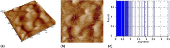
AFM always was used to analyze the parameters of surface topography and grains, as well as gather 3-D (three-dimensional) parameters, such as profile peaks and dents, for its high resolution and clear images. Reference Alexander, Marina, Bohuslav, Milan, Martin, Petr and Martin14 Figure 2(a) shows that the diamond film surface covered with islands of the remaining adsorbed molecules that were retained in the sampling range of 10,000 × 10,000 nm. To research for material 3-D microstructures, the root mean square of S q, surface skewness of S sk, surface kurtosis of S ku, ten point height of S z were used as the main parameters of morphology, which were listed in Table I. In Table I, (i) S q was the standard deviation of Z values within the sampling range, Z was point height. (ii) S sk was a nondimensional quantify, which was typically evaluated in terms of positive or negative, when the S sk was zero, an even distribution of data around the mean data plane was suggested; when the S sk was nonzero, an asymmetric, one-tailed distribution was suggested, such as flat plane having a small and sharp spike was greater than 0, or small, deep pit was less than 0; (iii) S ku was nondimensional quality used to evaluate the shape of data about a central mean. (iv) S z was the average difference in height between the five highest peaks and five lowest valleys relative to the mean plane. Reference Anirudha, Gilbert, David, Andrew, Mike, James, Tatyana, Shlomo and Robert15
AFM analysis of diamond film. (a) AFM topography, (b) grain sizes, (c) rate of grain sizes.

AFM analysis parameters of diamond film.

Table I shows that the S a, S q, S sk, S ku, S z of the diamond film was 79.2 nm, 99.7 nm, −0.236, 3.07, 740 nm, respectively. These parameters meant that the diamond film was smooth in general, while there were some deep pits on the film, the peaks on the surface distributed evenly and the surface was close to the Gaussian surface, the S ku value was 3. The minimum, maximum, and average grain area in the sampling range was 190.7 nm2, 3.609 × 10⁵ nm2, and 1.796 × 10⁵ nm2, respectively, shown in Fig. 2(b). The mean grain diameter was 478.2 nm, which can benefit improving hardness and mechanical properties of the diamond film, most of grain sizes were in the range of 0–106 nm2, as shown in Fig. 2(c).
C. Analysis of phases and structures
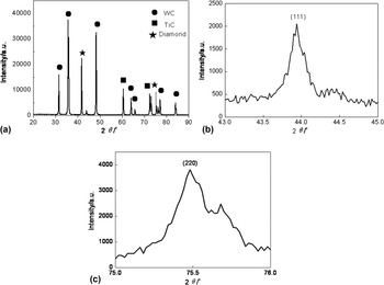
Figure 3 shows the XRD patterns of the films. Eleven peaks were found in the spectra at different 2θ values in Fig. 3(a). The XRD spectrum was dominated by two intense peaks located at 2θ = 43.8, 75.3°, which was identified with the reflection form (111) and (220) planes of diamond films. The diamond film had complete crystal structure and its lattice parameters were consisted with natural diamond. Reference Chowdury, Laugier and Henry16 The (111) plane [Fig. 3(b)] was more intense than (220) plane [Fig. 3(c)], which revealed that the crystal shape was mainly (111) plane. The full width at half maximum of (111) peak was small, which meant that the diamond film had good quality. In addition, the WC and TiC peaks also were observed at the XRD spectra, coming from the WC and TiC in the substrate.
XRD spectra of diamond film. (a) XRD spectrum, (b) C (111) spectrum, (c) C (220) spectrum.

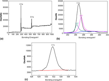
Figure 4 shows the photoemission spectra of the diamond film and XPS peaks of C1s and O1s. The C in the diamond film had four chemical states, such as C–H, diamond-like carbon (DLC), diamond, and C–O, the corresponding binding energy was 285 eV, 286 eV, 287 eV, 289 eV, respectively. Reference Ran and Zhen17 Figure 4(a) revealed that there were C1s and O1s peaks, the film was composed of C element and little O element, the existence of O element had been explained in Paragraph 3.1. In Fig. 4(b), the C1s spectrum was deconvoluted using two peaks corresponding to sp 3 bonded carbon (diamond) at the bonding energy of 285.4 eV, and sp 2 bonded carbon (graphite) at the bonding energy of 284.3 eV. The O1s peak with O2− existed at 531.82 eV, Reference Wang, Hu, Li, Li, Liu, Wang, Fu and Wang18 as shown in Fig. 4(c).
XPS spectra of diamond film. (a) Whole spectrum, (b) C1s, (c) O1s.

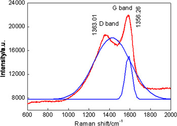
Raman spectrum of the diamond film is presented in Fig. 5. The diamond film was composed of a tetrahedral structure of sp 3 bonds [Fig. 4(b)], the Raman spectra was presented at 1363.01 cm−1, called G line. The highly oriented pyrolytic graphite was composed of sp 2 bonds [Fig. 4(b)], with planar triangular structure, and the Raman spectra was presented at 1556.26 cm−1, called G line.
Raman spectrum of diamond film.

D. Mechanical properties
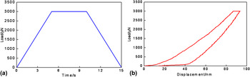
Figure 6(a) shows the curve of loads versus time in the nanoindentation, where the maximum load was 3000 N and the time was 15 s. Figure 6(b) shows that the relationships of loads versus time, it can be found that there were some discontinuities in smooth load–displacement curve. Near these discontinuities, the load declined rapidly and displacement increased slowly, the curve became smooth again if loading continuously. This was POP-IN phenomenon, Reference Kong and Fu19 it was always caused by phase transition, breakage, and peeling of the material. Reference Fan, Nose, Diao and Yoshida20 In this study, it was caused by breakage of diamond film. The cracks appeared on the film surface, which resulted in stiffness of film-substrate decreasing rapidly when the load reached the critical load of the film. The phenomenon led to the discontinuities in the load–displacement curve. A clearly discontinuous area appeared when the displacement was about 60 nm, which meant that a ring crack induced by high tensile radial stress on the film surface. In addition, a slight discontinuous area appeared when the displacement was about 28 nm, which meant that radial cracks were caused by high tensile stress on the film near the interface. The maximum load and maximum displacement were 3000 μN and 86.69 nm, respectively; meanwhile, residual displacement after unloading was 12.41 nm. The hardness (H) and elastic modulus (E r) of the diamond film was 16.27397 GPa and 166.1791 GPa, respectively.
Nanondentation curve of diamond film. (a) Loads versus time, (b) loads versus displacements.

E. Bonding strength and mechanism
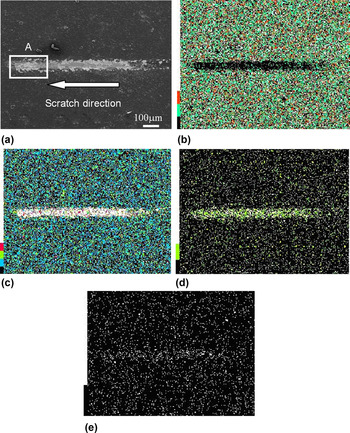
The binding strength of the diamond film was measured with a scratch test. A hemispherical indenter with the diameter of 200 μm scratched on the film surface, the film began peel off when the pressure reached a certain value, which was the critical load. When the film was scratched or peeled by the indenter, the audible signals were generated and caught by a sensor. Thus, the starting point of the signal was the point reaching the critical load, i.e., bonding strength. Reference Jiang, Luo, long, Hu, Li and Wang21 The SEM image of the scratch is shown in Fig 7(a), a light white stripe was deepened on the film and became wider gradually from right to left, which meant that the pressure increased when the indenter moved from right to left. The C concentration on the scratch decreased after scratching in Fig. 7(b), showing that the scratch was processed in the film. The concentrations of W, Ti, and Co increased in Figs. 7(c)–7(e), indicating that the scratched strip was the substrate surface after scratching, and the film had failed and spelled from the substrate.
Morphology and plane scans of scratch. (a) Scratch morphology, (b) C content, (c) W content, (d) Ti content, (e) Co content.

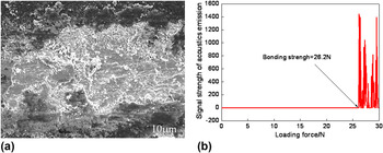
Figure 8(a) shows the fracture morphology of the film surface, there was a clear cleavage step, and directly peeled off from the substrate. The condition of film interface failure was shown as follows Reference Agarwal and Rao22 :
 $${\tau _{\max }} = {\tau _{{\rm{cr}}}} - k{\sigma _{\tau {\rm{,cr}}}}\quad ,$$
where τmax was the maximum shearing stress at interface; τcr was shearing stress at interface; k was a constant; and στ,cr was interfacial compressive stress.
Fracture morphology and bonding strength of diamond film. (a) Fracture morphology, (b) bonding strength.

From Eq. (1), it can be seen that the interface shearing stress of τcr was inherent in the film, and when the interface compressive stress of στ,cr was reasonably controlled during the deposition process, the maximum shearing stress of τmax could be reduced that achieved the purpose of improving bonding strength. When the shearing stresses of τmax was bigger than bonding force of the film–substrate interface, the film crazes, warped, or fell off. The failure modes of film were four as follows Reference Buijnsters, Shankar, Enckevort, Schermer and Meulen23 : (i) delamination flaking, the behavior occurred under tensile and compressive stress; (ii) the surface micro-crack or bridge crack expanded into its interface in the perpendicular to the surface, resulting in the film peel off from the substrate; (iii) blowing up occurred in the micro-crack or partial separation of the film–substrate interface, when the compressive stress exceeded the critical blowing stress, the blowing up appeared. (iv) The interaction of blowing up and delamination flaking. Because of compressive residual stress action, the film blowing up occurred; the substrate edge might result in separation of the film–substrate. Reference Toque, Herliansyah, Hamdi, Ide-Ektessabi and Sopyan24,Reference Gauthier, Durier and Fond25 From Fig. 8(a), it can be known that the scratching end of diamond film was expressed with the mixed morphologies of peeling off and brittle breakage, under the critical load. The difference of stress concentration, tensile stress, and the interfacial shearing stresses was bigger than its bonding strength; therefore, the interaction of the failure mechanism of above (iii) and (iv) was led to peeling off and breakage of the film.
The AE signal was observed at the load of 26.2 N, as shown in Fig. 8(b), which was bonding strength of the diamond film.
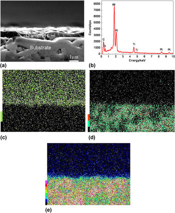
The interfacial bonding mechanism was analyzed with plane and line scans of the diamond film interface. Figure 9(a) shows the interface morphology of the diamond film–substrate. There was an obvious boundary between the film and substrate. The upper dark layer was diamond film with the thickness about 500 nm; the lower layer with bright white was the substrate of YT14. Figure 9(b) shows the result of plane scans, the mass fractions of chemical elements were shown as follows (mass%): C 12.48, O 16.83, Ti 19.66, and W 51.03; the corresponding atom fractions were shown as follows (at.%): C 33.69, O 34.11, Ti 13.31, and W 18.89. The mass fraction of C element was 40.01%, higher than that at the interface, while that of Ti and W was 6.99%, 16.18%, respectively, lower than that at the interface, respectively. In addition, there was O element at the interface. The EDS spectra at the interface mainly reflected the substrate compositions, thus the mass fractions of Ti and W increased, while that of the C element decreased. The existence of O element was caused by the oxidation of Ti element during the polishing. The layered distributions of C, W, and Ti elements were obtained in Figs. 9(c)–9(e). The W and Ti elements were enriched in the substrate, while the C element was enriched in the diamond films.
Interface morphologies and EDS spectra of diamond film. (a) Interface morphology, (b) result of plane scans, (c) C content, (d) W content, (e) Ti content.

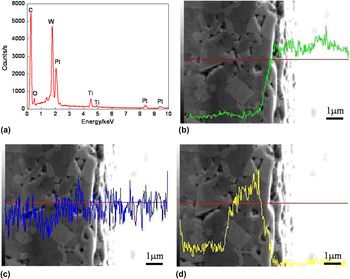
Figure 10(a) shows the result of line scans at the film interface, the mass fractions of chemical elements were shown as follows (mass%): C 69.22, Ti 7.42, W 23.36; and the atom fractions were shown as follows (at.%): C 93.19, Ti 2.50, W 4.31. The C atoms with the high content diffused at the interface, and the C content decreased in the direction of the substrate, as shown in Fig. 10(b). Because the C element had strong dispersal ability and higher diffusion speed to the film at the beginning stage of forming film, but the dispersal ability and diffusion speed of C atoms decreased rapidly after a certain distance. For this reason, the C content in the film at the bonding interface was higher than that in the substrate. On the contrary, the W and Ti elements were mostly concentrated in the substrate and diffused slightly, as shown at Figs. 10(c) and 10(d). It revealed that there were few O atoms in the film in Fig. 10(a), which was ignored, coming from: (i) there was little residual O2 in vapor chamber and involved into the reaction and entered into the films, (ii) the O atoms in the substrate reacted with the C atoms in the films, and the Ti atoms in the substrate and generated TiO2, which improved wear resistance of the films.
Line scan analysis of chemical elements at diamond film interface. (a) Result of line scans, (b) C content, (c) W content, (d) Ti content.

The interfacial modes were divided into three types, Reference Kerans, Jero and Parthasarathy26 i.e., mutation, compound, and proliferation: (i) when there was no diffusion of chemical reaction and proliferation, the mutant interface formed; when the compound formed near the interface, and the compound-type interface gained; and when there was a certain degree of solubility between the two modes, the diffusion interface obtained. From the view of interfacial bonding strength, the mutation interface was the worst, the compounded interface and the diffusion interface were the best. The plane scans and line scans shows that there was no obvious interface layer, the diamond film and substrate mixed each other near the interface, showing that the interface was diffusion-type and compound-type interface with the higher bonding strength.
IV. CONCLUSIONS
-
(1) The XRD peak of the diamond film at 2θ of 43.8 and 75.3° is corresponded to the diamond (111) plane and (220) plane, respectively.
-
(2) The surface roughness of the diamond film is 79.2 nm, and the corresponding gain sizes are in the range of 0–106 nm2.
-
(3) The C1s peak exhibits two main components such as sp 2 at the Raman shift of 1363.01 cm−1 and sp 3 at the Raman shift of 1556.26 cm−1.
-
(4) The hardness and elastic modulus of the diamond film by nanoindentation is 16.27397 GPa and 166.1791 GPa, respectively, and bonding strength of the diamond film is 26.2 N by scratch test.
ACKNOWLEDGMENTS
Financial support for this research by the Jiangsu Province Science and Technology Support Program (Industry) (BE2014818) is gratefully acknowledged.