Introduction
Conventional wireless transmitters necessitate separate oscillator-antenna configurations. Recent advances in co-design methodologies integrate these functional blocks into unified topologies, termed self-oscillating active integrated antennas (AIAs), delivering significant benefits in miniaturization, high integration, and manufacturing economy. Such integrated solutions have demonstrated critical utility across wireless power transfer (WPT) [Reference Wu and Ma1, Reference Huang and Ma2], radio frequency identification [Reference Adhikary, Biswas and Akhtar3–Reference Liu, Chang and Ma5], etc.
Many techniques have been implemented to enhance the oscillation and radiation performance of self-oscillating AIAs, including cross-coupled pair [Reference Tsai, Chu and Ma6, Reference Ma, Wu, Yeh and Chu7], electrically small conical folded dipole antenna [Reference Ramon, Bernal, Armanious, Tyo, Skipper and Abdalla8], backward-radiating helical antenna [Reference Tyo, Skipper, Abdalla and Martin9], substrate integrated waveguide (SIW) [Reference Adhikary, Sahoo, Biswas and Akhtar10], composite right-/left-handed (CRLH) resonator [Reference Ma, Wu, Yeh and Chu11], circuit multiplexing [Reference Du, Zhou, Liu and Guo12], and coherent stimulated emission [Reference Du, Li, Cui, Zhang and Sievenpiper13, Reference Du, Cui, Zhang, Guo, Zhang and Zhang14]. The cross-coupled pair of transistors embedded with LC resonators can achieve harmonic suppression in the self-oscillating AIA, which reduces the DC power consumption [Reference Ma, Wu, Yeh and Chu7]. The SIW technique is employed in [Reference Adhikary, Sahoo, Biswas and Akhtar10] to design a self-diplexing antenna in the self-oscillating AIA, which realizes concurrent dual-frequency signal generation and radiation. In [Reference Ma, Wu, Yeh and Chu11], a high-quality (Q) factor CRLH resonator is used to excite the radiator to boost its effective isotropic radiated power. In [Reference Du, Zhou, Liu and Guo12], a self-oscillating circuit is embedded and multiplexed in a dual-loop radiator to achieve dual-band operation. In [Reference Du, Cui, Zhang, Guo, Zhang and Zhang14], an extensible self-oscillating AIA array is designed based on coherent stimulated emission theory, which is able to boost the power level of the output pulse.
Reconfigurable techniques have been implemented in self-oscillating AIA designs to enhance controllability [Reference Wu and Ma15–Reference Singh, Basu and Koul20]. In [Reference Lin and Ma16], diodes are used to change the resonant frequency of the radiators, enabling the self-oscillating AIA to achieve frequency reconfigurability. In [Reference Singh, Basu and Koul18], several PIN diodes are inserted between two patch antennas and several delay lines, which control the phase of the current on the two antennas to obtain three radiation beams. PIN diodes are also embedded at four corners of the radiating element to control the shape of the patch antenna, which enables polarization reconfigurability of the feedback loop oscillator-type AIA in [Reference Singh, Basu and Koul20]. However, these self-oscillating AIAs are fundamentally limited to continuous wave (CW) generation with restricted operating power.
In contrast to the existing polarization reconfiguration methods for CW self-oscillating AIA, this work introduces a novel polarization reconfiguration approach applicable to pulsed self-oscillating AIA based on a pulse-triggered network. The proposed design integrates a reconfigurable pulse-triggered network with a dual-polarized radiator. This integration not only facilitates the direct conversion of direct current (DC) energy into radiated pulses within a highly integrated system but also enables polarization reconfigurability. The dual-polarized radiator serves dual roles as both the DC energy storage element and the radiator for the pulse-triggered network, supporting pulse oscillation and radiation with the desired polarization characteristics.
Design of the pulse transmitter
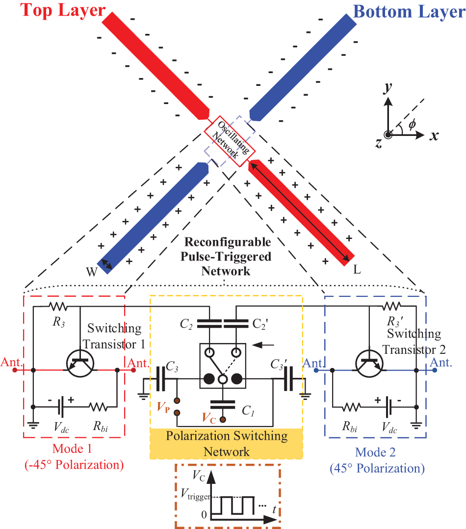
The proposed polarization-reconfigurable pulse transmitter integrates a dual-polarized dipole radiator with a reconfigurable pulse-triggered network, as illustrated in Fig. 1. The pulse transmitter is a periodic pulse source in which each working cycle consists of a charging phase and an oscillating phase. The reconfigurable pulse-triggered network aims to charge the dipole radiator during the charging phase and stimulate pulse oscillation and radiation during the oscillating phase. Specifically, when the switching transistor (Switching transistor 1 or Switching transistor 2) is off, which isolates the two arms of the dipole radiator, electric charges can be accumulated in the dipole radiator working as a capacitor (charging phase). The switching transistors are controlled by a low-frequency control signal V C through a polarization-switching network. When V C changes to a high-level voltage that activates the switching transistor to be on, the dipole radiator would be short-circuited, and the current oscillates on the radiator, and pulse radiation occurs (oscillating phase). Moreover, the polarization switching network is controlled by another bias voltage V p in order to selectively trigger the switching transistor 1 (mode 1, dipole radiator on the top layer with −45° polarization) or switching transistor 2 (mode 2, dipole radiator on the bottom layer with 45° polarization) for pulse oscillation and radiation in the desired polarization direction, thus enabling polarization reconfigurability. In order to improve the isolation between the two polarizations, both arms of the dipole radiators are sharpened to remove the overlapping areas between the two dipole radiators, thereby reducing the coupling effect.
Schematic diagram of the proposed integrated polarization-reconfigurable pulse transmitter.

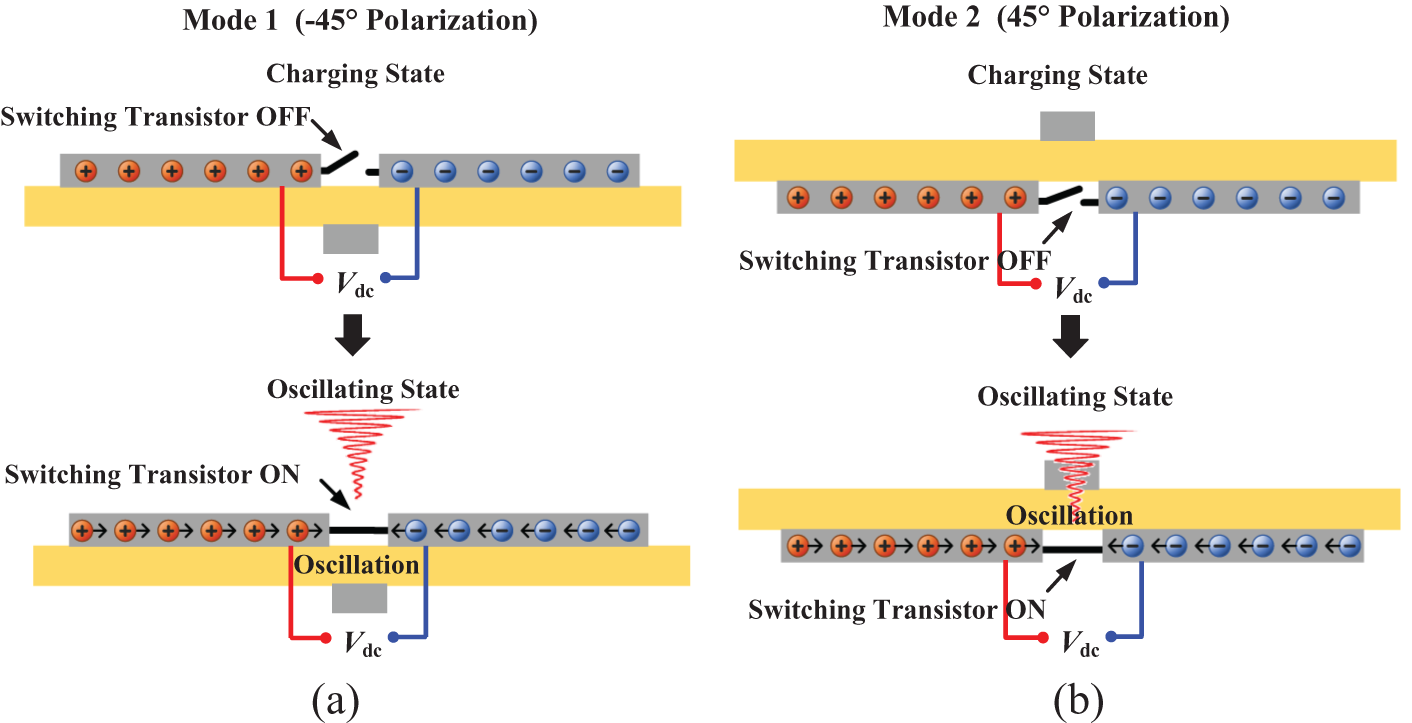
The working process of the proposed pulse transmitter is detailed as follows. Each switching transistor is embedded between the two arms of a dipole radiator. It is first in the off state to enable the pulse transmitter to work in the charging phase, as depicted in Fig. 2(a). In this case, the dipole radiators would be first charged by the DC power supply V DC through the bias resistors R bi in order to store the energy within the capacitive region of the radiators. Then, the polarization switching network will introduce a control signal V c to one of the switching transistors to switch the pulse transmitter from the charging phase to the oscillating phase. Specifically, once the voltage of the control signal reaches the threshold voltage V trigger, the target switching transistor would be activated, and the two arms of the corresponding dipole radiator would be suddenly connected. As a result, an oscillating current would be generated on the radiator, and a pulse would be radiated. In this way, the stored DC energy could be converted into a radiation pulse with a specific polarization. When the voltage of the control signal drops back to 0, the switching transistor becomes off, and the dipole radiator would be charged again, entering the next charging-oscillating cycle. The pulse repetition period is consistent with the operating cycle of the switching transistor, which is determined by the control signal V C. Moreover, the frequency of the oscillation and radiation of the pulse is determined by the resonant frequency of the dipole radiator, as well as the intrinsic capacitance and parasitic elements of the switching transistor.
Working principle of the proposed pulse transmitter operating in (a) mode 1 and (b) mode 2.

The polarization switching network in the reconfigurable pulse-triggered network is expected to enable the transition between two operating modes of the proposed design, thereby achieving polarization reconfigurability. It is designed to activate the target switching transistor and excite the pulse transmitter to generate radiation pulses with the desired polarization. In the switching network shown in Fig. 1(a), a SPDT switch is used, which is connected to the two switching transistors through the capacitors C 2 and C 2’, respectively. It introduces the control signal V C from its RFC port and transmits the control signal to activate the target switching transistor. The SPDT switch is controlled by the bias voltage V P. When the bias voltage V P is set to a high voltage level, the pulse transmitter would work in mode 1, where the electric charges oscillate in the dipole radiator on the top layer, generating an oscillating current that radiates a pulse with −45° polarization, as shown in Fig. 2(a). When VC turns to a low voltage level, the pulse transmitter would transition to mode 2, where the oscillating current would be generated in the dipole radiator on the bottom layer, resulting in the emission of a pulse with 45° polarization, as shown in Fig. 2(b). In this way, the proposed pulse transmitter achieves polarization reconfigurability.
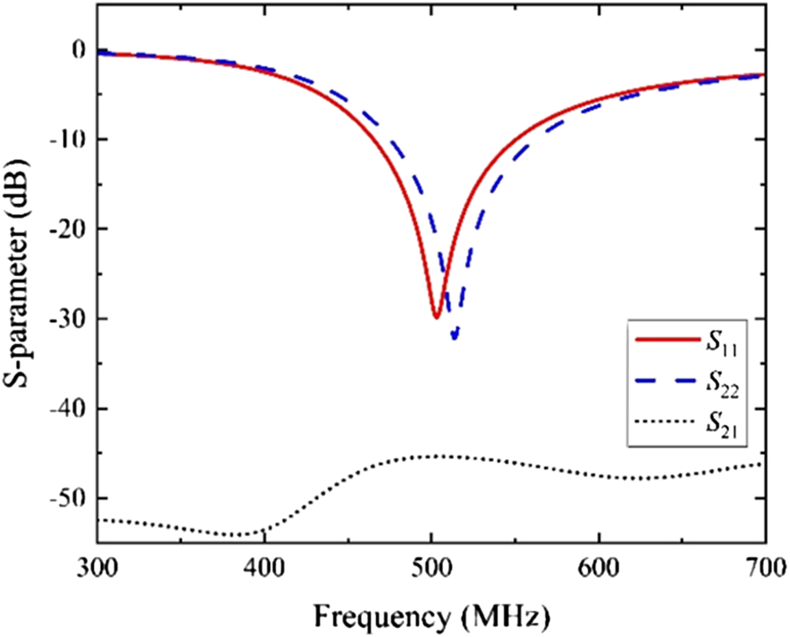
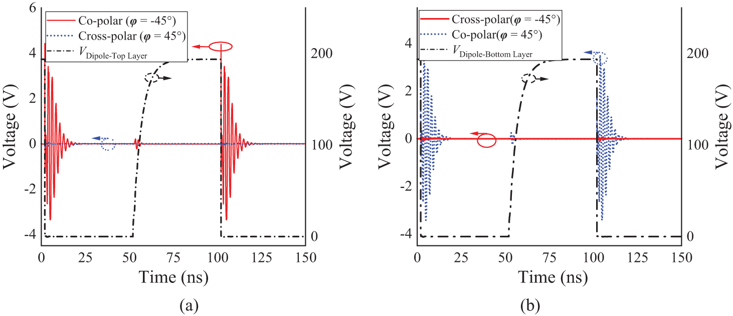
The polarization-reconfigurable pulse transmitter is designed on the FR4 substrate with a thickness of 1.2 mm, dielectric constants of 4.4, and a loss tangent of 0.02. In this example, the dual-polarized radiator is designed to work at 500 MHz. The length of each arm of the dipole radiator is determined by the resonant frequency of the passive dipole radiator, which is 126 mm. The width of each arm is optimized to ensure a sufficiently large equivalent capacitance of the antenna, consequently ensuring a large DC energy storage capacity for high output pulse voltage in the co-polar direction, while avoiding an increase in the cross-polar radiation. The width of each arm in this design example is set to be 8.5 mm. In order to obtain the performance of the radiator, the excitation ports are used to replace the pulse-triggered network, which is set between the two arms of the dipole radiators. The simulated S-parameters of the passive dual-polarized radiator are shown in Fig. 3, and the radiation patterns with realized gain are shown in Fig. 4. As seen, good isolation and orthogonal polarization are achieved. In addition, the surface current distributions of the radiator at the two operating modes are depicted in Fig. 5. Subsequently, in order to further simulate the pulse transmitter, ideal voltage-controlled switches are utilized in the simulation, which combines the full-wave simulator and circuit simulator. A control signal V C with a period of 100 ns and a duty cycle of 50% is used. Fig. 6(a) shows the simulated results of the proposed pulse transmitter working in mode 1 when V P is set to a high voltage level. As seen, the dipole radiator on the top layer is first charged, as indicated by V Dipole-Top layer (e.g., 52–102 ns), and then is short-circuited for pulse oscillation and radiation (e.g., 102–152 ns) during each working cycle. The pulse repetition period of the proposed design is 100 ns, which is the same as the control signal V C. Moreover, the pulse with −45° polarization is radiated with negligible cross polarization (45°). When V P is set to a low voltage level, the proposed pulse transmitter is reconfigured to work in mode 2, as shown in Fig. 6(b). Oscillation and radiation occur in the dipole radiator on the bottom layer, and the pulse with 45° polarization is radiated with negligible cross polarization (−45°). In addition, the efficiency of the pulse transmitter is calculated to be about 37% according to the periodic transient signal.
S-parameter of the passive dual-polarized radiator.

Radiation patterns with the realized gain of the dual-polarized radiator when the pulse transmitter works in mode 1 and mode 2.

Surface current density distributions of the radiator when the proposed design works in (a) mode 1 and (b) mode 2.

(a) Simulated potential difference VDipole-Top layer across the dipole radiator on the top layer and the radiated pulses when the pulse transmitter works in mode 1 (co-polar: φ = −45°; cross-polar: φ = 45°), as well as (b) the VDipole-Bottom layer and the radiated pulses in mode 2 (cross-polar: φ = −45°; co-polar: φ = 45°).

Implementation and experiment
To implement the proposed design, the avalanche transistor FMMT413 is adopted as the switching transistor in the reconfigurable pulse-triggered network, so as to switch the operating state of the pulse transmitter between the charging phase and the oscillating phase. The fabricated pulse transmitter and the details of the reconfigurable pulse-triggered network are presented in Fig. 7. In the experiment, the DC power supply V DC of 165 V is applied to charge the dipole radiators and bias the transistor FMMT413 to the critical avalanche state. It should be noted that the bias voltage across the avalanche transistor should be a little bit lower than the breakdown voltage of the transistor to ensure the critical breakdown state. Under this condition, the avalanche transistor can be triggered by the control signal to break down and short-circuit the two arms of the dipole radiator, thereby generating oscillation and radiation. The resistors R 1 and R 1’ with large resistance are deployed in parallel at the base of the transistors to avoid current passing through the base. Besides, in the polarization switching network, the GaAs switch HMC544, with the advantage of low insertion loss (Typ. 0.25 dB) and high isolation (Typ. 23 dB), is chosen as the SPDT switch. The capacitors C 1, C 2, and C 2’ are all 47 pF for the DC block, while the filtering capacitors C 3 and C 3’ are both 10 nF. A rectangular wave is introduced as the control signal V C by the polarization switching network to trigger the target avalanche transistor for oscillation and radiation with the desired polarization. The period, duty cycle, and amplitude of the rectangular wave are 50 µs, 50%, and 1.5 V, respectively.
(a) Photograph of the fabricated pulse transmitter, and the (b) top view and (c) bottom view of the reconfigurable pulse-triggered network.

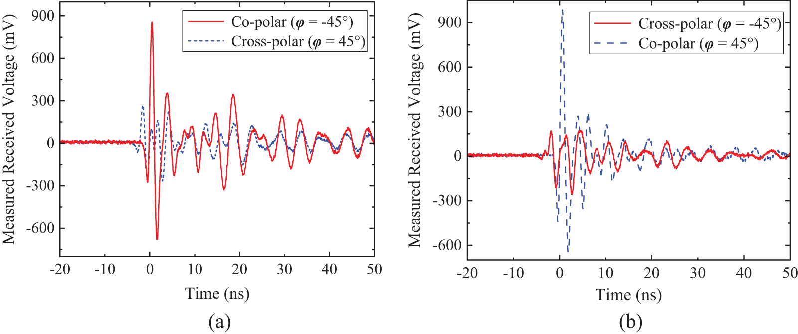
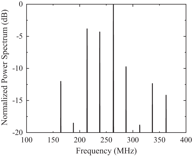
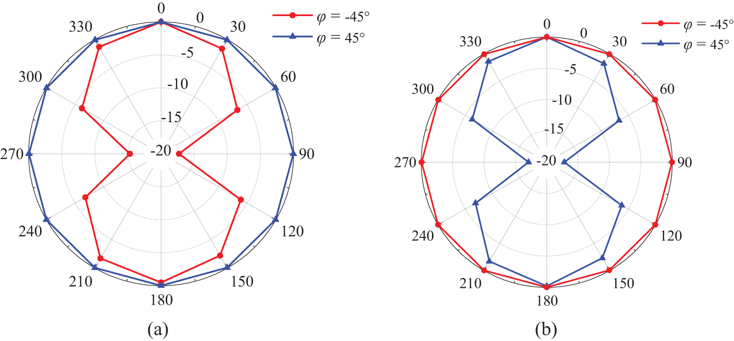
In the measurement, a standard horn antenna is used as a receiving antenna at a distance of 1.5 m to capture the radiated pulses and transmit the waves to an oscilloscope. The received pulse when the proposed pulse transmitter is working in mode 1 is shown in Fig. 8(a). As observed, the co-polarization of the radiated pulse occurs at a polarization angle of −45° with a peak-to-peak voltage of 1.6 V. By changing the bias voltage V P, the pulse transmitter transitions to mode 2. As seen from Fig. 8(b), the co-polarization of the radiated pulse changes to the polarization angle of 45°, while the peak-to-peak voltage remains about 1.6 V. Moreover, the power spectrum of the pulses is presented in Fig. 9. As seen, the center frequency of the radiated pulse is about 265 MHz, which depends on the resonant frequency of the passive dipole radiator, as well as the intrinsic capacitance and parasitic elements of the switching transistor, that is, the avalanche transistor FMMT413 used in this test prototype. Note that there are two ways to suppress the undesired frequency components if needed, including adding transmission zeros to the radiator and using cavities or waveguides to house the pulse transmitter. Furthermore, the normalized radiation patterns of the proposed pulse transmitter working in mode 1 and mode 2 are shown in Fig. 10, which agree well with the simulated results.
Received pulses from the proposed pulse transmitter working in (a) mode 1 (co-polar: φ = −45°; cross-polar: φ = 45°) and (b) mode 2 (cross-polar: φ = −45°; co-polar: φ = 45°), respectively.

Normalized measured power spectrum of the received pulses from the pulse transmitter.

Normalized radiation patterns of the proposed pulse transmitter working in (a) mode 1 and (b) mode 2.

The comparison among the proposed pulse transmitter based on the self-oscillating AIA and the state-of-the-art self-oscillating AIAs is presented in Table 1. The proposed pulse transmitter based on the self-oscillating AIA can achieve polarization reconfigurability with a competitive high output voltage. Moreover, unlike conventional designs that employ PIN diodes for polarization switching in low-power CW self-oscillating AIA [Reference Singh, Basu and Koul20], this work presents a method that achieves polarization reconfigurability in high-voltage pulsed self-oscillating AIAs.
Comparison with state-of-the-art self-oscillating AIAs

a Calculated from the received power levels (Pr) given in the literature.
b AIA unit cell.
Conclusion
A polarization-reconfigurable pulse transmitter utilizing a pulse-triggered network has been designed and experimentally validated. This transmitter features a highly integrated structure and operates in two distinct modes corresponding to two orthogonal polarizations. It is capable of directly converting DC energy into radiated pulses with reconfigurable polarization, featuring compact size, low cost, and light weight. It is suitable for applications such as electric effects testing and electro-magnetic interference (EMI).
Acknowledgements
This work was supported by the State Key Laboratory of Millimeter Waves (grant number K202416).
Competing interests
The authors report no conflict of interest.
Author contributions
Manman Cui derived the theory, performed the simulations, and wrote the paper. Jun-Hao Lai performed the simulations and measurements. Huai-Tian Zhou performed the simulations and analyzed data.

Manman Cui received the B.Eng. Degree from the Xi’an University of Technology, Xi’an, China, in 2011, and the Ph.D. degree from the South China University of Technology, Guangzhou, China, in 2018, respectively. She is currently a lecturer with the Guangzhou University of Chinese Medicine, Guangzhou, China. Her current research interests include wireless power transfer, wireless communication networks, SWIPT systems, and medical IoT.

Jun-Hao Lai received the B.S. degree in electronic science and technology from Guangdong University of Technology, Guangzhou, China, in 2024, where he is currently pursuing an M.S. degree with the School of Integrated Circuits. His research interests include self-oscillating active integrated antenna and retrodirective antenna.

Huai-Tian Zhou received the B.S. degree in electronic information science and technology from Huizhou University, Huizhou, China, in 2022. He received the M.S. degree from the School of Information Engineering, Guangdong University of Technology, Guangzhou, China, in 2025. He currently works as a professional engineer at Samsung Electronics. His research interests include self-oscillating active integrated antenna.