I. INTRODUCTION
Plasmonics is currently a very actively studied areaReference Dionne and Atwater1 as the combined nature of the electric and photonic excitation inherent in a surface plasmon mode allows manipulation of photons in nanophotonics, integrated plasmonic circuits, antennas, optical imaging and quantum information transfer.Reference Dionne and Atwater1 In this article we focus on plasmonic and photonic structures to enhance the performance of thin film silicon-based solar cells.
The common solar cell architecture for thin film silicon solar cells usually utilizes a micromorph architecture composed of a top cell of high band gap amorphous silicon (a-Si:H) followed by a bottom cell of hydrogenated nanocrystalline silicon (nc-Si:H).Reference Schropp and Zeman2–Reference Yue, Sivec, Owens, Yan, Yang and Guha4 The red and near-infrared (IR) photons of longer wave lengths are absorbed in the bottom cell, whereas the top cell absorbs the shorter wave lengths, with current matching between the cells. A ubiquitous problem in all silicon-based solar cells is the poor absorption of red and near-IR photons of longer wave lengths.Reference Schropp and Zeman2–Reference Battaglia, Escarre, Soderstrom, Erni, Ding, Bugnon, Billet, Boccard, Barraud, DeWolf, Haug, Despeisse and Ballif5 The absorption length of these photons exceeds the thickness of the nc-Si:H layer (typically 1 μm), and the quantum efficiency of these solar cells decreases rapidly at wave lengths near the band edge (1.1 μm in nc-Si:H).Reference Schropp and Zeman2–Reference Yue, Sivec, Owens, Yan, Yang and Guha4
Similar problems are well known in a-Si:H solar cells where the active layer thickness is limited by the hole diffusion length (which is ∼300 nm). The absorption length of red and near-IR photons with wave length λ > 650 nm exceeds the thickness of the a-Si:H cell- hence light trapping is essential. Crystalline silicon solar cells have even lower absorption than a-Si:H or nc-Si, and have poor absorption and quantum efficiency at red and IR wave lengths (λ > 700 nm) upto the Si band edge.
To harvest photons more efficiently, light trapping strategies can be used. Two competing light-trapping approaches have emerged. The traditional approach uses a randomly roughened back reflector (BR)Reference Dionne and Atwater1, Reference Yue, Sivec, Owens, Yan, Yang and Guha4, Reference Yue, Sivec, Yan, Yang, Guha, Wang, Yan, Flewitt, Tsai and Higashi6 in substrate nip cells or a textured zinc oxide (ZnO) front scattering layer in superstrate pin cells on glass.Reference Isabella, Krc and Zeman7, Reference Battaglia, Escarré, Soderstrom, Charrière, Despeisse, Haug and Ballif8 However, the second and recent approach involves using periodic photonic crystal or plasmonic crystal back reflectors.Reference Ferry, Verschuuren, Li, Walters, Schropp, Atwater and Polman9–Reference Tan, Santbergen, Smets and Zeman16
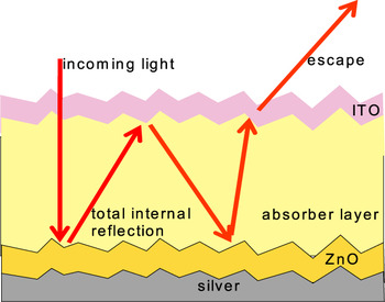
Randomly textured back reflectors are fabricated by annealing silver (Ag)/zinc oxide (ZnO) into a random distribution of islands, or by etching ZnO and coating with Ag/ZnO. Randomly textured BRs scatter light stochastically at the back reflector, through all angles, and thereby increase the path length of photons within the absorber layer. Each scattering event is an independent process. If the incident angle at the top interface exceeds the critical angle, light is trapped; otherwise the light escapes (Fig. 1). Light rays are fully randomized within the thin absorber layer. For an ideal “loss-less” Lambertian scattering surface, which reflects incoming light uniformly into all angles, the enhancement factor of the path length inside the absorber layer has a limiting value of 4n2,Reference Yablonovitch17 where n is the wave length-dependent refractive index. This factor can be derived by summing up the trapped rays,Reference Tiedje, Yablonovitch, Cody and Brooks18 or very elegantly by comparing the area of the escape cone with the complete phase space i.e., the surface area of the sphere for modes within the semiconductor layer.Reference Schiff19 It is a current challenge to develop BRs that approach and exceed the Lambertian 4n2 limit.Reference Schiff19, Reference Biswas and Xu20 The 4n2 limit has a value ∼45 for silicon whereas it is only ∼12–14 for organic semiconductors. The 4n2 Lambertian limit was derived with “loss-less” conditions- an idealization of real back reflectors. It assumes that there is no reflection lossReference Yablonovitch17, Reference Tiedje, Yablonovitch, Cody and Brooks18 from the front surface of the solar cell, which is also difficult to achieve in practice. This classical Lambertian 4n2 limit was commonly believed to have the best achievable light-trapping. However, recent fundamental light-trapping theory has indicated that this limit can be overcome.Reference Yu, Raman and Fan21 It is known that roughened Ag/ZnO structures suffer from intrinsic losses of several percent at each reflectionReference Springer, Poruba, Mullerova, Vanecek, Kluth and Rech22 that lead to large losses for weakly absorbed photons when multiple reflections from the back reflector occur.
Schematic depiction of the light trapping generated by a randomly textured back reflector, showing trapped and escaping rays.

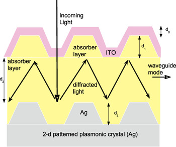
The alternative approach of a periodically textured back reflector i.e., photonic crystal (Fig. 2), has been recently developed.Reference Ferry, Verschuuren, Li, Walters, Schropp, Atwater and Polman9, Reference Ferry, Verschuuren, Li, Schropp, Atwater and Polman13, Reference Ferry, Verschuuren, van Lare, Schropp, Atwater and Polman14, Reference Biswas and Xu20, Reference Zhou and Biswas23 The periodic photonic crystal strongly diffracts light into wave guided modes (Fig. 2) traversing in the plane of the structure where they are absorbed. In addition, the periodic back reflector with a “connected” metal layer leads to surface plasmon modes, where the light intensity is strongly enhanced, and very strongly absorbed. Alternatively back reflectors formed by arrays of “disconnected” silver nanoparticles on a substrate layer (such as ZnO), have been recently studiedReference Dionne and Atwater1, Reference Gusak, Kasemo and Hagglund15, Reference Tan, Santbergen, Smets and Zeman16 and enhancement is observed from both plasmonic light concentration and strong scattering of light.
Schematic depiction of the light trapping generated by a periodic back reflector, showing strongly diffracted light and waveguide modes within the absorber layer.

A crucial question is whether periodic back reflectors are superior to random back reflectors and if so over what range of wave lengths? The answer to this question is examined first through simulation and design where we design periodic back reflectors that can absorb at or beyond the Lambertian (4n2) limit. The second approach is to experimentally fabricate random and periodic back reflectorsReference Bhattacharya, Chakravarty, Pattnaik, Slafer, Biswas and Dalal12 on identical device architectures and examine the device performance of these cells. Although we discuss nip substrate cells in this study, we note that periodic ZnO structures formed by nanomoldingReference Battaglia, Escarré, Soderstrom, Charrière, Despeisse, Haug and Ballif8 have very successfully exhibited photocurrents comparable to or exceeding random structures in pin superstrate solar cells, where the front texture is responsible for random scattering of light into the absorber layer.
II. DESIGN PRINCIPLES FOR PERIODIC BACK REFLECTORS
Three basic design principles are involved in periodic back reflectors: The first design principle is the strong “photonic” diffraction of waves by the periodic back reflector. To understand this we consider the random back reflector first. Random back reflectors function by scattering light through random angles at each reflection from the back surface. If the angle of incidence at the top surface of the absorber layer is smaller than the critical angle the light ray will be lost in the escape cone at the top surface. If the incidence angle is greater than the critical angle the light ray is trapped inside. As seen in Fig. 1, after multiple reflections a ray can escape from the top surface.
The behavior of the periodic back reflector (Fig. 2) is markedly different as the entire wave front is “coherent” and hence all points within the wave front behave in the “same way.” The modes within a thin layer are reflected from the top and bottom of the absorber layer and are trapped in the layer when the round trip phase difference Δφ is a multiple of 2π (Δφ = 2πm), where m is an integer.Reference Biswas and Xu20, Reference Zhou and Biswas23, Reference Bermel, Luo, Zeng, Kimerling and Joannopoulos24 Such modes traverse parallel to the interface in a coherent manner. The entire wave front is “coherent” so that no further scattering can occur to extract the wave from the top surface. The coherence can only be broken by defects. This type of propagation parallel to the interface cannot occur in a random back reflector.
The second design principle involves the formation of surface “plasmon” modes at the interface of the metal and semiconductor absorber layer. These surface plasmon modes are longitudinal (with E || k), where E is the electric field and k the propagation vector, and have large field intensity in the absorber layer and also field intensity in the metal.Reference Atwater and Polman25, Reference Pillai, Catchpole, Trupke and Green26 The enhanced surface plasmon field is extended over a much longer region in the semiconductor absorber, leading to enhanced absorption. In solar cells, electric fields within a small interfacial region in the metal can occur, which could cause losses. The surface plasmon mode for a bare Ag surface occurs at 320 nm. However for a flat metal-semiconductor surface it is shifted to the near-IR approximated by εs + 2εm = 1, where εs and εm denote the dielectric functions of the semiconductor and metal respectively. The surface plasmon modes couple to the diffracted wave guide modes in the periodic system.
As noted by previous authors,Reference Dahal, Sainju, Li, Stoke, Podraza, Deng and Collins27 “localized” (nonpropagating) surface plasmons also are generated within the randomly textured back reflectors. Generally these may be lossy but under appropriate conditions, these may reradiate.Reference Springer, Poruba, Mullerova, Vanecek, Kluth and Rech22
The third design principle is an antireflection coating that allows all the light to enter the cell without reflection loss. This is an important practical consideration, as the Lambertian 4n2 limit assumes a perfect antireflection coating i.e., all incident light enters the solar cell without reflection loss. A single quarter-wave-length antireflection layer, such as a top indium tin oxide (ITO) layer, is only optimized for a single wave length (usually in the green ∼550 nm), and suffers reflection losses at both the short and long wave-length region. It is necessary to have a tapered surface that grades the refractive index from the silicon value to the air value, thereby providing an optical impedance match between the high index absorber layer and air and minimize reflection loss. We have achieved such a tapering in the conformal solar cell described below.
III. THEORY AND SIMULATION APPROACH
Our simulations are based on a well-established scattering matrix methodReference Li and Lin28 where Maxwell’s equations are solved in Fourier space i.e., in a basis of plane waves for both polarizations of the incident wave. The solar cell (Fig. 1) is divided into a number of layers in the z-direction. In each layer the dielectric function is a periodic function of x, and y but not of z. Realistic wave-length-dependent dielectric functions are used for Ag, and nc-Si:HReference Dionne and Atwater1 from experimental measurement. Maxwell’s equations are integrated with the correct boundary conditions throughout the unit cell to obtain the scattering matrices of each layer and the entire structure. From the scattering matrix we find the total reflectance R (including diffracted beams) and transmission T (which is 0) at each incident wave length. The absorption at each wave length is then A = 1-R-T. Details have been covered in previous publications.Reference Li and Lin28
We characterize solar cell architectures by their weighted absorption <Aw>,
 $$\lt A_w \!\!>\, = \int_{\lambda _1 }^{\lambda _2 } {A(\lambda ){{dI} \over {d\lambda }}} d\lambda \quad,$$
and short-circuit current Jsc,
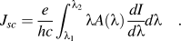 $$J_{sc} = {e \over {hc}}\int_{\lambda _1 }^{\lambda _2 } {\lambda A(\lambda ){{dI} \over {d\lambda }}} d\lambda \quad.$$
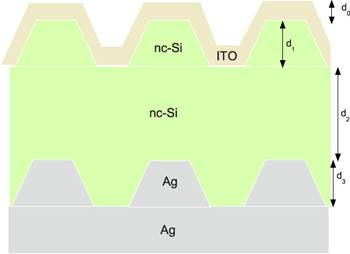
These periodic back reflectors have been carefully designed with rigorous solutions of Maxwell’s equations,Reference Biswas and Xu20 to optimize light absorption and short-circuit current. We have developed a novel conformal solar cell architecture (Fig. 3) consisting of a back reflector of tapered metallic nanopillars, in a periodic plasmonic crystal (PC) array, with pitch a. The nc-Si:H absorber layer conforms to this array and is followed by an antireflection coating of ITO of thickness d0, and is an architecture that we fabricated (Fig. 4).
Schematic conformal solar cell architecture with a tapered array of nanopillars as the back reflector, depicted in a planar cross-section. The nanopillars form a two-dimensional triangular lattice.

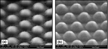
SEM images of a (a) nanoimprinted polymer substrate before coating a (b) nanoimprinted substrate with the periodic array of tapered nanopillars coated with Ag and ZnO. The pitch is 750 nm, and the pillar height 180 nm.

A triangular lattice plasmonic crystal is chosen following our previous work, which found this array to be an optimum structure.Reference Biswas and Xu20, Reference Zhou and Biswas23 The nanopillars are coated with silver- the preferred reflecting material. We vary the pitch a, thickness d0, height of the front corrugation d1, height of the back reflector nanocylinders d3, and thickness d2 of the absorber layer, to find the optimum light absorption. For simplification we ignore the thin ZnO layer between the Ag and nc-Si:H.
Nanoimprint lithography at LightWave Power was used (Fig. 4) to fabricateReference Bhattacharya, Chakravarty, Pattnaik, Slafer, Biswas and Dalal12 the periodic polymer nanostructure (Fig. 4) that was coated with Ag and ZnO to achieve back-reflection. A similar nanopillar- and nanohole array have been fabricated by nanoimprint lithography, for solar cell growth. Thus the simulations were performed to optimize a class of structures that were fabricated with nanoimprint lithography. We have deposited 1-μm thick nc-Si:H solar cells on such textured substrates with a nanopillar height of 180 nm.
IV. SIMULATION RESULTS
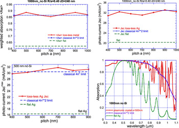
We have rigorously designed and simulated a conformal solar cell structure, that optimizes optical absorption and is comparable to the Lambertian limit (4n2 limit), with scattering matrix simulations. We rigorously simulated (Fig. 5) the absorption and short-circuit current Jsc for a conformal solar cell with an nc-Si:H absorber layer thickness of 1000 nm, typical of micromorph cells.
(a) Weighted absorption for 1000 nm nc-Si:H and (b) simulated photocurrent for 1000 nm nc-Si:H absorber layer as a function of the lattice pitch of the periodic back reflector. The simulated absorption is averaged over the entire range of absorption 400–1100 nm. Shown for comparison are the Lambertian limit and the the flat Ag mirror. (c) The photocurrent of a 500 nm nc-Si:H absorber layer. (d) Simulated absorption as a function of wavelength for the 1000 nm nc-Si:H absorber layer compared with the Lambertian 4n 2 limit and the flat Ag mirror.

For comparison with the classical 4n2 limit, which assumes loss-less conditions, we show results with a nearly loss-less metal as the back reflector. We find configurations (a ∼ 500 nm, a ∼ 900 nm) where the weighted absorption of the conformal solar cell exceeds the classical 4n2 limit, over the “entire” spectral range (400–1100 nm). Jsc is very close to the classical limit at the pitch a ∼ 500 nm and slightly above the limit at a ∼ 900 nm (Jsc = 33.08 mA/cm2). There is a very large enhancement of 43% for <Aw> and 61% for Jsc over the flat silver back reflector (Jsc = 20.5 mA/cm2).
We also show simulations for a 500-nm nc-Si:H layer and find that the photocurrent can be at the 4n2 limit and is slightly above the Lambertian limit for a pitch near 700 nm [Fig. 5(c)] by ∼1 mA/cm2. Enhancement factors are larger as the thickness is decreased. We find that the losses in the back reflector are ∼5%, but vary with the selected pitch, with smaller losses for larger pitch. We have verified that using very small pitch (a < 100 nm) corresponding to very small nanoparticles results in very high parasitic absorption in the metal back reflector, and should be avoided in practice.
The optimal configuration is quite sensitive to the nanopillar height and an optimum near 220-nm height is indicated. The enhancement over the classical limit becomes even more pronounced as the absorber layer thickness is decreased. The short-circuit current is at or slightly above the classical 4n2 limit (Fig. 5) for 500- to 1000-nm thick nc-Si:H, common thicknesses utilized in micromorph solar cells. For larger thickness the classical limit is higher than the plasmonic crystal (Fig. 5).
The wave-length-dependent absorption A(λ) for the conformal PC back reflector [Fig. 5(d)] considerably improves over the flat Ag back reflector at wave lengths above 600 nm, and below 450 nm, and is very successful in collecting photons throughout the red and near-IR range (600–1100 nm). The PC absorption exceeds the classical 4n2 limit at many wave lengths in this near-IR region, due to the absorption maxima arising from diffraction resonances i.e., wave guide modes or from surface-plasmon polaritons at the back reflector.
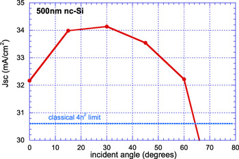
We also found that the absorption significantly exceeds the 4n2 Lambertian limit, when light is incident at an angleReference Biswas and Xu20 (Fig. 6). The simulation suggests that periodic back reflectors can generate absorption at or even exceeding the Lambertian limit. The conical surface is effective in channeling light more effectively when incident at an angle. There is a marked increase of absorption, which is significantly above the 4n2 limit.
Absorption as a function of incident angle for periodic nanocone back reflector arrays.

V. PATTERNED DIELECTRIC BACK REFLECTORS
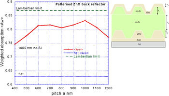
It has been a long-standing debate in the area of randomly roughened substrates whether randomly roughened Ag is preferable to roughened ZnO on Ag. An alternative approach to a patterned metallic back reflector is to pattern a dielectric layer of ZnO at the back reflector so that the cones of Ag are replaced by the cones of ZnO on a base of ZnO resulting in the structure Ag/ZnO/patterned ZnO/nc-Si/conformal ITO. The refractive index contrast between Si and ZnO is ∼3.6/2 = 1.8 which is significant for photonic effects. The patterned ZnO diffracts the light into the absorber layer. Such patterned dielectrics do not show plasmonic light concentration and at the same time avoids losses associated with plasmonic fields generated in the metal. Accordingly we simulate the performance of patterned ZnO layers. The thickness of the base ZnO layer should be near a quarter wave length to maximize reflection into the absorber layer, and we find it to be ∼50 nm. We find that the analogous back reflector crystal of periodic ZnO nanocones shows substantial absorption enhancement, but lower than the Lambertian limit (Fig. 7). The best-optimized back reflector has a pitch near 1000 nm close to the band edge. The patterned ZnO structure has lower absorption than the patterned metallic back reflector, but at the same time has less parasitic absorption.
Absorption as a function of pitch of a patterned ZnO back reflector of nanocones, compared with the flat and Lambertian limit. The schematic structure used is shown in the inset.

VI. EXPERIMENTAL INVESTIGATIONS OF ENHANCED SOLAR CELLS
Photons absorbed in the intrinsic layer generate photoexcited carriers that are collected and observed in quantum efficiency and I–V measurements on solar cells. Such experimental investigations of nip solar cells determine the carrier collection processes “in addition” to the absorption of light, and provide results on carrier transport that are not possible to be generated by simulation alone. We experimentally measure the enhancement of solar cells by the periodic back reflectors. We experimentally compare the performance of periodic and randomly roughened substrates for nip solar cells fabricated under identical conditions.
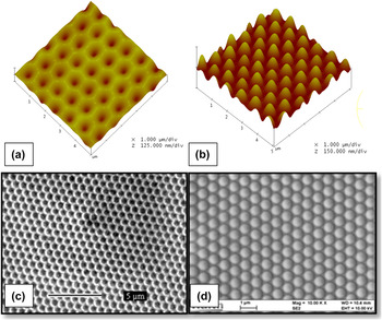
Nanoimprint lithography was used to fabricate periodic nanocone arrays and nanohole arrays at LightWave Power. The pitch of these arrays was ∼750 nm for nc-Si:H, and scanning electron microscopy (SEM) and atomic force microscopy (AFM) images for the structures showing excellent order over large areas (Fig. 8). As designed through simulations, the nanopillars are tapered at the top surface, which is evident in the AFM image shown in Fig. 8(a). We have grown n-i-p nc-Si:H devices on (i) stainless steel, (ii) flat Ag on stainless steel, (iii) Annealed Ag/ZnO substrate, (iv) etched Ag/ZnO, and the (v) photonic plasmonic nanoarray. We utilize a conventional 70-nm thick ITO layer at the top of the cell as an antireflection coating. The identical device architecture and similar thickness (1.0 μm) was used so that the devices on different substrates could be meaningfully compared. All solar cells grow conformally with the top surface of the cell displaying the pattern of the substrate. SEM images on top of the ITO (Fig. 8), after the solar cell was deposited, demonstrate nanopillar features are preserved after nc-Si:H and ITO deposition. This conformal top surface has excellent antireflective properties with the grading from silicon to air.
AFM images of (a) nanohole periodic BR (a), (b) nanopillar and SEM images (c) the nanohole BR and (d) nanopillar.

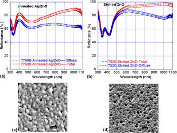
(a) Total and diffuse reflectance measured for the annealed Ag/ZnO substrate, using an integrating sphere. (b) Total and diffuse reflectance measured for the etched ZnO substrate. (c) The SEM image of an annealed Ag substrate and the (d) SEM image of etched ZnO substrate.

For the randomly roughened substrates, we selected randomly roughened Ag/ZnO and etched ZnO/Ag substrates with very high diffuse reflectance (Fig. 9), exceeding 70% over the entire wave-length range, comparable to the state of the art. The total reflectance approaches 90% at long wave length. The typical feature size in the random back reflectors exceeds 1 μm. The annealed Ag shows randomly distributed protrusions, whereas the etched ZnO shows complementary randomly distributed crater-like structures (Fig. 9), formed by etching.
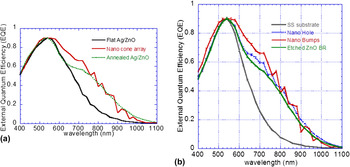
(a) Measured EQE as a function of wave length for nc-Si:H solar cells on the flat Ag/ZnO, randomly roughened Ag/ZnO and the nanobump photonic–plasmonic substrate. (b) Measured EQE as a function of wave length for nc-Si:H solar cells on the stainless steel substrate, nanohole array randomly etched ZnO, and the nanobump substrate.

We measured the external quantum efficiency (EQE) for the various solar cells as a function of wave length (Fig. 10), and show the comparison in two separate panels [Figs. 10(a) and 10(b)] for clarity. Clearly the nanocone substrate has the highest EQE over most of the wave-length range. For wave lengths below ∼900 nm the nanocone array BR has higher EQE than the randomly roughened annealed Ag/ZnO, both of which show considerable enhancements over the flat Ag/ZnO substrate [Fig. 5(a)]. Above 900 nm, the annealed Ag/ZnO has slightly higher EQE than the nanocone BR [Fig. 5(b)]. We observed that the nanocone substrate has higher EQE than both the nanohole and etched Ag/ZnO BR for wave lengths below 900 nm, but slightly lower EQE for the same above 900 nm. It is likely that this wave length of 900 nm can be adjusted by changing the lattice pitch. The fluctuations of the values of EQE as a function of wave length in the periodic back reflectors (nanobump and nanohole array), arise from the diffractive resonances or wave-guided modes generated by the periodic back reflector,Reference Biswas and Xu20, Reference Bermel, Luo, Zeng, Kimerling and Joannopoulos24 where the light propagation is parallel to the layers, generating maxima in the absorption as discussed in our previous theoretical work.Reference Biswas and Xu20, Reference Zhou and Biswas23
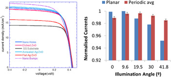
We measured the photocurrent and I-V characteristics (Fig. 11) and found that the nanopillar back reflector clearly provided the highest current (21.5 mA/cm2), significantly larger than the randomly textured back reflectors (20.4 mA/cm2, for annealed Ag) and the flat back reflector. The I-V characteristics (Fig. 11) also show the open-circuit voltage (0.47 V) and fill factor of these devices. We measured the angular dependence of the photocurrent [Fig. 11(b)] on the incident angle of illumination to understand further the theoretically predicted response of absorption with angle (Fig. 5). We observe that the absorption is less affected by illumination angle with a maximum absorption near 20°. In contrast, the absorption decreases monotonically with angle for the flat BR. Although the change in absorption with angle is less than the prediction, further measurements are needed for other cells for validating any inference.
(a) Current–voltage characteristics (I–V) for all the cells fabricated on periodic randomly textured and flat substrates. (b) Photocurrent measured as a function of incident angle for a planar solar cell and the periodic nanocone back reflector solar cell. Currents are normalized to their maximum values for both cases, respectively.

VII. DISCUSSION
In recent studies, both the photocurrent and efficiency of n-i-p a-Si:H solar cells for a self-assembled array of plasmonic Ag nanoparticles on a ZnO/Ag back reflectorReference Tan, Santbergen, Smets and Zeman16 or a periodic array of Ag nanoparticles on AgReference Ferry, Verschuuren, van Lare, Schropp, Atwater and Polman14 are found to be larger than that of a randomly textured ZnO/Ag back reflector, strengthening the conclusion that photonic or plasmonic back reflectors can exceed the performance of randomly roughened back reflectors. The Ag cones of the back reflector used in the n-i-p a-Si:H cellReference Ferry, Verschuuren, van Lare, Schropp, Atwater and Polman14 are similar to those discussed in our study, except for a smaller pitch (400–500 nm) than in our work.
The experimental solar cells have lower enhancement than theoretical predictions. One reason for this is the thick n-layers. Another factor is the ZnO layer on the patterned Ag. The plasmonic enhancements are largest in the vicinity of the Ag interface and much of the plasmonic enhancement can be lost both within the ZnO layer, and the thick n-layer, at the back of the cell. To maximize the plasmonic enhancement, the back n+ layer, and the interfacial ZnO layer should be very thin so that the plasmonic light concentration occurs in the absorber layer, rather than in an inactive portion of the solar cellReference Haug, Soderstrom, Naqavi and Ballif29 that does not generate photocurrent. Our devices had relatively thick back n+ layers, ∼0.2 μm. This was done to avoid shorts, especially in the highly corrugated nanopillar geometry. As the maxima of the electric field intensity is near the Ag it is highly desirable to have as thin a n-layer as possible. State of the art pin solar cells have in fact achieved n-layer thicknesses of 20–50 nm. By using recently developed n-doped SiOx, realization of a thin n-layer is also more feasible.Reference Yue, Yan, Sivec, Su, Zhou, Yang, Guha, Yan, Gleskova, Tsai, Sameshima and Cohen30 We have measured the device parameters as the n-layer thickness is decreased from 200 to ∼80 nm for “flat” devices on SS and found that the fill factor (FF) and open-circuit photovoltage (VOC) both increase by ∼5% as the thickness decreases. Our calculations estimate that the best effects are obtained when the back n+ layer thickness is <100 nm.
It is also necessary to use a thin (80–100 nm) interfacial ZnO layer between the Ag and nc-Si, to eliminate interdiffusion of Ag in Si. For simplicity this ZnO layer has not been included in the present simulations. However other recent mode coupling simulationsReference Haug, Soderstrom, Naqavi and Ballif29 have included the effect of the ZnO layer and found that the plasmonic resonance frequency shifts to shorter wave length as the ZnO thickness is increased. In the absence of the ZnO interfacial layer, for a corrugated Ag–Si interface, the lowest order mode is a p-polarized surface plasmon mode that appears below the silicon light line. However in the presence of the ZnO layer the mode converts to a regular wave-guided mode located above the silicon light line.Reference Haug, Soderstrom, Naqavi and Ballif29 This is an aspect for further theoretical and experimental study.
We chose an absorber layer thickness of 1 μm, typical for micromorph cells, and our expectation is that these conclusions will be observed for other cell thicknesses. Although surface plasmons can cause losses in random back reflectors, it has been proposed that a substantial fraction of light coupled into localized plasmonic modes at the Ag/ZnO interface can be reradiated as scattered light in optimized textured back reflectors, and dynamical effects need further understanding.
The combination of random features as well as periodic features is a very interesting direction to explore. We have preliminary experimental resultsReference Pattnaik, Chakravarty, Slafer, Biswas, Dalal, Yan, Gleskova, Tsai, Sameshima and Cohen31 that do not show enhancements when random structures are superimposed on periodic structures, but further work is needed in this area, especially to understand effects of correlated randomness. It is likely that the periodic back reflector structure demonstrated in this article can be extended to other materials including crystalline silicon and organic solar cells.
VIII. CONCLUSIONS
In conclusion we have fabricated a well-controlled series of nc-Si:H solar cells on both photonic-plasmonic back reflectors and randomly textured back reflectors. The randomly textured BRs were chosen to have very high diffuse reflectance. The periodic BR of photonic plasmonic nanostructures out-performs the best annealed silver randomly textured back reflector, even though our device structure is not optimized for plasmonic effects, illustrating the viability of the periodic structure for advanced photon harvesting. Further work is necessary to quantify losses occurring within the solar cell, and redesigning cells to reduce such losses.
ACKNOWLEDGMENTS
This research was supported by the Ames Laboratory, operated for the Department of Energy by Iowa State University under Contract No. DE-AC0207CH11385 (computational studies); by the Iowa Power Fund (experimental studies) and EECS-0824091 (experimental studies). We thank our colleagues at Microelectronic Research Center, for their experimental help. We thank our collaborators at LightWave Power (D. Slafer and J. Ji) for the nanoimprinting.