I. INTRODUCTION
Research on two-dimensional atomic crystals and heterostructures has grown enormously in the last decade, sparked by the properties of monolayers being different than properties of the bulk, to become one of the leading sub-fields in condensed matter physics and materials science. Reference Geim1,Reference Wang, Kalantar-Zadeh, Kis, Coleman and Strano2 The wavefunction of a monolayer extends beyond its surface, decaying exponentially into the materials (or vacuum) both above and below it. The surface (if vacuum) or interface (in a heterostructure) interactions result in structural distortions, new phenomena, new physics, and challenging chemistry. For example, MoS2 transitions from an indirect to a direct band gap semiconductor, Reference Wang, Yuan, Hong, Li and Cui3 the onset temperature of superconductivity in 2H–NbSe2 decreases as the number of NbSe2 layers is decreased and in extremely thin samples of NbSe2 superconductivity no longer persists, Reference El-Bana, Wolverson, Russo, Balakrishnan, Paul and Bending4 and ultrathin layers of PbSe distort from the bulk rock salt structure, with both a puckering distortion and a pairing interaction between layers. Reference Anderson, Heideman, Lin, Smeller, Kokenyesi, Herzing, Anderson, Keszler, Zschack and Johnson5 While stability issues have limited the ability to prepare monolayer films of many materials via a cleaving approach, Reference Geim and Grigorieva6 the ability to reasonably predict the structure of potential heterostructures made from 2-D atomic constituents makes them attractive candidates for theoretical investigations that predict properties as a function of nanoarchitecture. There are already quite a few predictions of interesting properties reported in the literature. Reference Zeng, Wang, Fu, Gong, Zhou, Ajayan, Lou and Liu7,Reference Qian, Liu, Fu and Li8
The interaction at the interfaces between monolayers also provides interesting experimental opportunities to both tailor existing properties and potentially obtain properties not found in either of the constituent materials. It has already been shown that the properties of graphene strongly depend on the substrate on which it is grown. Reference Yang, Chen, Shi, Liu, Zhang, Xie, Cheng, Wang, Yang, Shi, Watanabe, Taniguchi, Yao, Zhang and Zhang9 Ultra low thermal conductivity results from rotational disorder between layers. Reference Heideman, Tepfer, Lin, Rostek, Zschack, Anderson, Anderson and Johnson10 Several reports of samples containing thin layers of VSe2 differ with respect to the effect of layer thickness on the charge density wave (CDW) that occurs at 100 K in the bulk single crystals. Reference Bayard and Sienko11 If prepared via liquid exfoliation, the CDW increases to 135 K (Ref. Reference Xu, Chen, Li, Wu, Guo, Zhao, Wu and Xie12) as thickness is reduced to 4–8 trilayers of VSe2. In micromechanically exofoliated VSe2 nanoflakes, the CDW onset temperature was reported to decrease to 11.6 nm at 81 K, the lowest thickness measured. Reference Yang, Wang, Liu, Du, Ning, Zheng, Jin, Han, Wang, Yang, Tian and Zhang13 In turbostratically disordered single layers of VSe2 separated by layers of SnSe prepared using a self-assembly approach, a CDW has been reported that has an opposite carrier type (holes) than the bulk (electrons), Reference Atkins, Disch, Jones, Haeusler, Grosse, Fischer, Neumann, Zschack and Johnson14 which does not occur when the VSe2 thickness is increased beyond a monolayer. Reference Falmbigl, Fiedler, Atkins, Fischer and Johnson15 An understanding of how to control properties based on the interaction between layers is developing as more heterostructures, and their properties are reported.
The change in carrier type and CDW reported for SnSe–VSe2 heterostructures relative to bulk VSe2 prompted us to prepare a new heterostructure consisting of alternating layers of BiSe and VSe2. BiSe was chosen as a companion layer due to the prior literature on BiSe–dichalcogenide misfit compounds, which showed that the transport properties of (BiSe)1.10NbSe2 and (BiSe)1.09TaSe2 are very similar to those of the analogous Sn compound. Reference Zhou, Meetsma, de Boer and Wiegers16 Localization of the additional valence electron of the Bi within the BiX subsystem has been proposed as a reason for the similar transport properties. Reference Wiegers17 The charge is localized in Bi–Bi bonds at anti-phase boundaries, which are thought to systematically occur due to the mutual accommodation of the lattice mismatch to form a commensurate structure. Reference Zhou, Meetsma, de Boer and Wiegers16,Reference Petříček, Cisarova, de Boer, Zhou, Meetsma, Wiegers and van Smaalen18 We find that the VSe2 layer(s) in a superlattice containing single layers of BiSe and VSe2 is structurally similar to what was previously reported for [(SnSe)1.15]1(VSe2)1. The in-plane diffraction pattern and layer positions from Rietveld refinement of the specular diffraction pattern are consistent with BiSe having a rocksalt type structure. High-angle annular dark-field scanning transmission electron microscopy (HAADF-STEM) images, however, reveal extensive turbostratic disorder and the presence of anti-phase boundaries seen previously in BiSe containing misfit layer compounds. This suggests that the presence of anti-phase boundaries are not dependent on forming an ordered long-range distortion of both constituent structures to form a coherent crystal. Despite the similarity of the structure of the VSe2 single layers, no CDW is observed in the BiSe–VSe2 heterostructure. The BiSe–VSe2 heterostructure has a negative Hall coefficient, indicating n-type carriers predominate, which is similar to bulk VSe2. Reference Bayard and Sienko11 Since [(SnSe)1.15] m (VSe2)1 heterostructures have positive Hall coefficients, indicating that holes are the predominant carrier, the change of carrier type in the BiSe–VSe2 heterostructure prevents formation of the CDW.
II. EXPERIMENTAL
The compound [(BiSe)1+δ]1(VSe2)1 was synthesized using the modulated elemental reactants (MERs) technique in a custom built high-vacuum physical vapor deposition chamber. Reference Fister19 Elemental sources of Bi (99.995%) and V (99.8%), obtained from Alfa Aesar (Haverhill, Massachusetts), were evaporated at a rate of 0.4 Å/s using Thermionics 3 kW electron-beam guns (Thermionics, Hayward, California) onto (100) oriented Si wafers. Se (99.999%) was deposited at a rate of 0.5 Å/s utilizing a Knudsen effusion cell. Rates were monitored using quartz crystal monitors positioned 25 cm above the elemental sources. A custom-made LabView program controlled the rotation of a carousel with mounted Si wafers over the desired elemental sources to obtain the desired deposition sequence. Pneumatically powered shutters allow a precise control of atomic composition based on the opening time of the shutter. The Se–Bi–Se–V layering sequence was repeated until a total thickness of 45–55 nm of the modulated precursor was obtained. To determine optimal annealing conditions for self-assembly, the precursors were annealed between 200 and 550 °C for 20 min. X-ray diffraction (XRD), discussed below, was used to determine optimal temperature.
To form the ferecrystalline products, the precursors were annealed for 20 min in a N2 glove box with oxygen content below 0.6 ppm and the resulting products characterized using x-ray scattering. XRD was performed to determine repeat unit thickness of the film. XRD measurements were performed on a Bruker D8 Discover diffractometer (Bruker Corporation, Billerica, Massachusetts) equipped with Cu Kα radiation, Göbel mirrors, and Bragg-Brentano optics geometry. Locked coupled θ–2θ scans were taken from 5–65° 2θ for XRD. Samples were prepared for STEM on a FEI Helios 600 dual-beam (FEI Company, Hillsboro, Oregon) using methods developed by Schaffer et al. Reference Schaffer, Schaffer and Ramasse20 HAADF-STEM images were taken on a FEI Titan 80-300 field emission gun transmission electron microscope (FEG-TEM) at the Center for Advanced Materials Characterization in Oregon (CAMCOR).
The van der Pauw technique Reference van der Pauw21 was used to determine temperature-dependent resistivity and Hall coefficient of the sample in a temperature range of 20–295 K. Samples for electrical resistivity and Hall measurements were deposited on fused Quartz crystal slides. Using a shadow mask, a 1 cm × 1 cm cross geometry was deposited and indium contacts were placed on the points of the cross. By sourcing a current between two adjacent contacts and measuring the voltage on the remaining two contacts, an average sheet resistance at a fixed temperature can be found.
 $$\rho = {{\pi d} \over {\ln 2}}{R_{{\rm{Avg,Sheet}}}}f\quad .$$
Resistivity, ρ, can be found by converting the average sheet resistance, R, into resistivity by using thickness (d) of the sample and the cross pattern symmetry (f). The Hall coefficient was also determined using the van der Pauw technique by sourcing a current of 100 mA between two opposing contacts, applying a magnetic field of 0–1.6 T, and measuring the voltage induced by the magnetic field between the two remaining opposing contacts. The Hall coefficient, R H, is the slope of the least squares fit for the measured voltage versus applied magnetic field curve.
III. RESULTS AND DISCUSSION
The [(BiSe)1+δ]1[VSe2]1 heterostructure was synthesized using MERs approach. In this approach, precursors consisting of a sequence of elemental layers are repeatedly deposited on a nominally room temperature substrate and then annealed to self-assemble the desired heterostructure. The sequence of elemental layers, in this case Se–Bi–Se–V was chosen to resemble that in the targeted heterostructure. The relative thicknesses of the elemental layers in the Bi–Se bilayer was calibrated to yield a one-to-one stoichiometry and the absolute thickness was calibrated to yield two (100) monolayers of a rock salt structured BiSe. The relative thicknesses of the elemental layers in the V–Se bilayer was calibrated to yield a 1–2 stoichiometry and the absolute thickness was calibrated to a single layer of a Se–V–Se dichalcogenide structure. The precursors were deposited using a previously described deposition system. Reference Fister19 Initial ratio of deposition thicknesses and absolute thicknesses of both Bi–Se and V–Se elemental bilayers to obtain a bilayer layer of BiSe and a structural monolayer of VSe2 were taken from previous studies. Reference Atkins, Disch, Jones, Haeusler, Grosse, Fischer, Neumann, Zschack and Johnson14,Reference Heideman, Nyugen, Hanni, Lin, Duncombe, Johnson and Zschack22 The initial samples self-assembled into the desired [(BiSe)1+δ]1[VSe2]1 compound after annealing at 350 °C for 20 min, but broader and less intense 00l diffraction maxima than seen in previous ferecrystals Reference Heideman, Tepfer, Lin, Rostek, Zschack, Anderson, Anderson and Johnson10,Reference Atkins, Disch, Jones, Haeusler, Grosse, Fischer, Neumann, Zschack and Johnson14,Reference Alemayehu, Falmbigl, Grosse, Ta, Fischer and Johnson23 were observed in a specular XRD scan. The lattice parameter was close, however, to the expected one, and only 00l reflections were observed in the specular scan, suggesting the formation of the desired compound crystallographically aligned with the c-axis perpendicular to the substrate. We varied the initial Bi composition in the BiSe component by 5% both above and below the ideal composition. The c-axis lattice parameter varied from 1.178(1) nm when Bi was deficient to 1.180(1) nm when there was excess Bi, and in both extremes the quality of XRD scans decreased, having larger line widths and less intensity than at the ideal composition. The Bi content that gave the largest intensity and smallest line-width was used in subsequent studies. The c-axis lattice parameters in all of the samples are smaller than the 1.203 Å observed for [(SnSe)1.15]1(VSe2)1. Reference Atkins, Disch, Jones, Haeusler, Grosse, Fischer, Neumann, Zschack and Johnson14
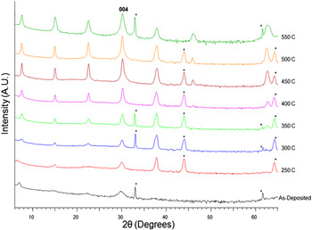
An annealing study was performed to determine optimal formation conditions and the resulting specular XRD scans are shown in Fig. 1. The as-deposited scan contains only broad (001) and (004) reflections. After 20 min of annealing at 250 °C, the first six (00l) reflections are observed, indicating the self-assembly of the targeted heterostructure. The intensity of these reflections increases and the line width decreases with increasing annealing temperature until 500 °C. After annealing at 550 °C, the line-widths begin to broaden due to evaporation of the components. An annealing period of 20 min at 500 °C was therefore chosen as the optimal annealing conditions.
A series of diffraction scans collected as a function of annealing temperature, as indicated at the right side of the scans. All of the diffraction peaks from the sample can be indexed as (00l) reflections and the (004) reflection is indexed in the figure. Diffraction artifacts from the stage and Si substrate are marked with * symbols.

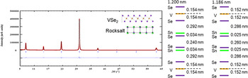
The specular diffraction pattern, Rietveld refinement and difference between them for the [(BiSe)1+δ]1[VSe2]1 heterostructure are shown in Fig. 2. The refined position of the atomic planes along the c-axis of the refined structure is compared to the previously reported structure for [(SnSe)1.15]1(VSe2)1 in the image below the data. The positions of the atomic planes are consistent with the expected heterostructure. The refined V–Se distance is 0.152(1) nm in the BiSe–VSe2 heterostructure, which is very similar to the 0.152(1) nm reported for [(SnSe)1.15]1(VSe2)1. Reference Atkins, Disch, Jones, Haeusler, Grosse, Fischer, Neumann, Zschack and Johnson14 The Bi and Se atoms in the BiSe layer are no longer in the same plane as would be expected for a rock salt structure, with the Bi closer to the Se layer in VSe2 by 0.025(1) nm. This “puckering” distortion is smaller than most reported, which range between 0.020 and 0.060(1) nm in previously reported rock salt-dichalcogenide misfit structures. Reference Wiegers17 In [(SnSe)1.15]1(VSe2)1, the Sn and Se planes are 0.034(1) nm apart, Reference Atkins, Disch, Jones, Haeusler, Grosse, Fischer, Neumann, Zschack and Johnson14 while a puckering of 0.0293(1) Reference Zhou, Meetsma, de Boer and Wiegers16 and 0.291(1) nm (Ref. Reference Petříček, Cisarova, de Boer, Zhou, Meetsma, Wiegers and van Smaalen18) has been reported in the misfit layer compound (BiSe)1.09TaSe2. Two selenium layers of the BiSe constituent are separated by a distance of 0.260(1) nm, which is quite smaller than 0.2751(1) and 0.2820(1) nm found by Zhou et al. Reference Zhou, Meetsma, de Boer and Wiegers16 in (BiSe)1.09TaSe2. This separation is much larger than the 0.24(1) nm found in [(SnSe)1.15]1(VSe2)1. Reference Atkins, Disch, Jones, Haeusler, Grosse, Fischer, Neumann, Zschack and Johnson14 Gap between Bi layer of the BiSe and VSe2 is 0.286(1) nm which is shorter than the 0.292(1) found in [(SnSe)1.15]1(VSe2)1. Reference Atkins, Disch, Jones, Haeusler, Grosse, Fischer, Neumann, Zschack and Johnson14 In (BiSe)1.09TaSe2, a gap of 0.3232 nm is found between the BiSe and the Se plane of TaSe2. Reference Petříček, Cisarova, de Boer, Zhou, Meetsma, Wiegers and van Smaalen18 A gap of 0.289(1) nm was reported in a recent paper containing the structure of a BiSe–NbSe2 heterostructure. Reference Mitchson, Falmbigl, Ditto and Johnson24 The refined model is consistent with the targeted BiSe–VSe2 heterostructure.
Rietveld refinement of the [(BiSe)1+δ]1[VSe2]1 heterostructure determine the position of atomic planes along the c-axis. The model to the right shows projected positions of the atoms onto the c-axis and their relative distances.

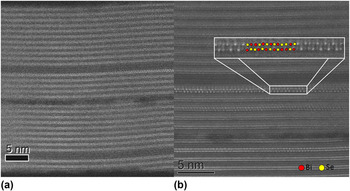
To obtain additional information about the [(BiSe)1+δ]1[VSe2]1 heterostructure, cross section HAADF-STEM images were collected and representative images are contained in Fig. 3. The structure from the top to the bottom of the film, Fig. 3(a), contains alternating layers of VSe2 and BiSe consistent with the targeted heterostructure. Occasionally, there are missing layers of BiSe suggesting that the precursor used for this STEM sample was deficient in Bi. These missing layers of BiSe, which reduce the coherence of the structure perpendicular to the substrate, are the likely cause of the line broadening observed in the specular diffraction patterns as composition was varied. In higher resolution images, some of the layers are aligned along the [111] and [100]/[010] zone axes, but the majority of the layers are not, consistent with prior reports of extensive rotational disorder between layers for samples prepared using MERs. Reference Grosse, Atkins, Kirmse, Mogilatenko, Neumann and Johnson25 Several images contain regions in which some of the BiSe layers are aligned along a zone axis, as shown in Fig. 3(b). Clearly visible in these layers is a periodic anti-phase boundary, similar to that previously reported for (BiSe)1.09TaSe2. Reference Zhou, Meetsma, de Boer and Wiegers16,Reference Petříček, Cisarova, de Boer, Zhou, Meetsma, Wiegers and van Smaalen18
(a) Representative cross section HAADF-STEM images of the [(BiSe)1+δ]1[VSe2]1 heterostructure. (b) Appearance of antiphase boundaries apparent in BiSe bilayer.

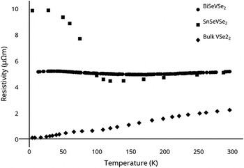
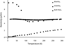
Resistivity as a function of temperature is shown in Fig. 4 for the [(BiSe)1+δ]1[VSe2]1 heterostructure prepared in this study along with that of bulk VSe2 (Ref. Reference Bayard and Sienko11) and [(SnSe)1.15]1(VSe2)1. Reference Atkins, Disch, Jones, Haeusler, Grosse, Fischer, Neumann, Zschack and Johnson14 The resistivity of the [(BiSe)1+δ]1[VSe2]1 heterostructure looks like that of a metal both in magnitude and in its temperature dependence. It has a very similar room temperature resistivity as [(SnSe)1.15]1(VSe2)1 (Ref. Reference Atkins, Disch, Jones, Haeusler, Grosse, Fischer, Neumann, Zschack and Johnson14) and 2.5 times higher resistivity than bulk VSe2. It has a more temperature independent resistivity than bulk VSe2, which is consistent with prior comparisons of heterostructures made using MERs with crystalline misfit layered compounds. Reference Alemayehu, Falmbigl, Grosse, Ta, Fischer and Johnson23 There is no evidence for the prominent CDW transition found for [(SnSe)1.15]1(VSe2)1 (Ref. Reference Atkins, Disch, Jones, Haeusler, Grosse, Fischer, Neumann, Zschack and Johnson14) in the resistivity data for the [(BiSe)1+δ]1[VSe2]1 heterostructure.
Resistivity data as a function of temperature for the [(BiSe)1+δ]1[VSe2]1 heterostructure compared to that reported for VSe2 (Ref. Reference Xu, Chen, Li, Wu, Guo, Zhao, Wu and Xie12) and [(SnSe)1.15]1(VSe2)1. Reference Atkins, Disch, Jones, Haeusler, Grosse, Fischer, Neumann, Zschack and Johnson14

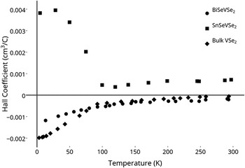
To obtain more information on the differences between the electrical properties of the [(BiSe)1+δ]1[VSe2]1 heterostructure, Hall coefficients were measured as a function of temperature as shown in Fig. 5. The measured Hall coefficient for the [(BiSe)1+δ]1[VSe2]1 heterostructure is negative, similar in magnitude and temperature dependence as that reported for bulk VSe2 (Ref. Reference Bayard and Sienko11) and for SnSe–VSe2 heterostructures prepared with thicker VSe2 layers. Reference Falmbigl, Fiedler, Atkins, Fischer and Johnson15 This contrasts with the positive Hall coefficient previously reported for [(SnSe)1.15]1(VSe2)1. Reference Atkins, Disch, Jones, Haeusler, Grosse, Fischer, Neumann, Zschack and Johnson14
Hall coefficients as a function of temperature for the [(BiSe)1+δ]1[VSe2]1 heterostructure compared to that reported for VSe2 (Ref. Reference Xu, Chen, Li, Wu, Guo, Zhao, Wu and Xie12) and [(SnSe)1.15]1(VSe2)1. Reference Atkins, Disch, Jones, Haeusler, Grosse, Fischer, Neumann, Zschack and Johnson14

The resistivity and Hall data reported here for the [(BiSe)1+δ]1[VSe2]1 heterostructure are distinctly different than that reported for the analogous SnSe compound as shown in Figs. 4 and 5. [(SnSe)1.15]1(VSe2)1 (Ref. Reference Falmbigl, Fiedler, Atkins, Fischer and Johnson15) is a p-type conductor and has a significant increase in resistivity and in the Hall coefficient consistent with a CDW transition. The [(BiSe)1+δ]1[VSe2]1 heterostructure is an n-type conductor and the temperature dependence of its Hall coefficient looks very similar to that of VSe2. The higher resistivity of the [(BiSe)1+δ]1[VSe2]1 heterostructure likely results from a higher concentration of defects than the equilibrium grown single crystal of VSe2.
There are several potential reasons for the difference in transport behavior between the [(BiSe)1+δ]1[VSe2]1 and the [(SnSe)1.15]1[VSe2]1 heterostructures. One unlikely explanation is that the V centers of the VSe2 layer in the [(BiSe)1+δ]1[VSe2]1 heterostructure adopt a trigonal prismatic coordination rather than the expected octahedral coordination found in the [(SnSe)1.15]1[VSe2]1 heterostructure and in bulk VSe2. The similarity of the bond distances between the V and Se layers in both heterostructures argues against this, although there is no direct evidence for the coordination of the V in the VSe2 layer. A second possibility is that a difference in the alignment of the electronic bands and the Fermi level of the SnSe and BiSe constituent with those of the VSe2 monolayer results in a different amount of charge transfer. The distortion of both the SnSe and BiSe bilayers in the [(MSe)1+δ]1[VSe2]1 heterostructures relative to their bulk structures indicates the importance of the interface in determining the structure and consequently the electronic structure. The periodic antiphase boundary in the BiSe bilayer has been proposed by Wiegers to localize potential conduction electrons in Bi–Bi bonds at the antiphase boundary in BiX containing misfit layer compounds as a means of rationalizing the trivalent nature of Bi determined from bond valence sum calculations with the similar electronic properties of analogous Sn containing misfit layer compound. Reference Wiegers17 A higher conductivity of the BiSe layer relative to that of SnSe might electronically couple with the VSe2 layers on either side of it more strongly, changing the electronic structure. The periodic changes in the interface potential resulting from the regular anti-phase boundaries in the BiSe layer might also prevent the formation of the CDW. The lack of CDW in crystalline misfit layer compounds has been proposed to result from the strong interaction between layers overwhelming the weaker electron–phonon interactions underlying CDW formation.
The modular design criteria inherent to heterostructures enable one to propose potential heterostructures to systematically test physical phenomena. For example, preparing a repeating structure consisting of a single structural unit of VSe2–BiSe–MoSe2–BiSe would maintain the same interfaces adjacent to the VSe2 layer, but the semiconducting MoSe2 layer would reduce the through plane conductivity. If electron localization is the driving force for the formation of antiphase boundaries in the BiSe bilayer, a VSe2–BiSe–VSe2–M1−x M′ x Se heterostructure where M and M′ had different valences would enable the titration of the charge density. The changing charge density might also be expected to change the frequency of the antiphase boundary. Comparing a VSe2–BiSe heterostructure with a VSe2–Bi2Se3 or a VSe2–PbSe heterostructure would probe the effect of the antiphase boundary on the CDW. Interest in heterostructures will continue to expand as theory and experiment are able to test ideas and concepts via systematic changes in nanostructure and nanoarchitecture.
IV. CONCLUSIONS
The single structural layer of VSe2 in the [(BiSe)1+δ]1[VSe2]1 heterostructure has very similar structural properties to that found in the analogous [(SnSe)1.15]1[VSe2]1 heterostructure, but the heterostructures have very different electrical properties. The [(BiSe)1+δ]1[VSe2]1 heterostructure is metallic with electrons as majority carriers while the analogous [(SnSe)1.15]1[VSe2]1 heterostructure has holes as the majority carriers. The [(SnSe)1.15]1[VSe2]1 heterostructure has large resistance and Hall coefficient change with temperature as a consequence of a CDW transition, while the [(BiSe)1+δ]1[VSe2]1 heterostructure has an almost temperature independent resistivity and a Hall coefficient sign (negative), magnitude and temperature dependence that is very similar to bulk VSe2. The major structural difference between the two heterostructures is in the MSe constituent. The bilayer of SnSe adopts a rock salt structure while the BiSe bilayer has periodic anti-phase boundaries resulting in a larger a-axis lattice parameter. The anti-phase boundaries are thought to both localize electrons in Bi–Bi bonds and potentially effectively scatter charge carriers, resulting in a low mobility. Systematic changes in heterostructure constituents and nanoarchitecture are suggested to further probe the effect of interfaces and charge transfer between constituents on properties.
ACKOWLEDGMENTS
We acknowledge support from the National Science Foundation under grant DMR-1266217. We also acknowledge support through the Collaborative Access Team (CAT): Pooled Resources for Electron Microscopy Informatics, Education and Research (PREMIER) Network Program at Pacific Northwest National Laboratory (PNNL) and the Environmental Molecular Sciences Laboratory, a national scientific user facility sponsored by DOE's Office of Biological and Environmental Research at PNNL. PNNL is a multiprogram national laboratory operated by Battelle for DOE under Contract DE-AC05-76RL01830.