Importance of power electronics
Developments in electronics have thus far been propelled especially by the field of information technology (IT). Improvements in energy savings and efficient usage of electric power are urgent issues for future sustainable development across technology areas. In the near future, a significant amount of renewable energy is anticipated to become available, and more efficient usage of motor-drives and other power-intensive applications is strongly desired. High-performance electric power converters for more efficient motor drives are in demand. Power electronics is a technology for the conversion and control of electric power for energy generation, transmission, storage, and consumption and is a promising technology for future electrical energy management.Reference Zacharias1 Moreover, electric energy networks are being developed in conjunction with information networks. Much more functionality can be expected for the sophisticated operation of electric energy in many of these areas, which will be increasingly important to society. Power electronics is expected to play an important role for these purposes.
This article presents a technology roadmap for power electronics utilizing wide bandgap semiconductors.Reference Okumura2 Based on this roadmap, recent progress in silicon carbide (SiC) semiconductor power electronics is reviewed, and future prospects are discussed.
Approaches to next-generation power electronics for the future
Power electronics can be applied to a wide range of fields, from IT equipment power supplies to electric power transmission systems. The semiconductor devices and circuits used exhibit a large variety in capacity, size, and function. In addition, special research and development (R&D) needs exist due to the extreme conditions specific to power electronics equipment, such as high reliability, high tolerance, as well as low loss compared with conventional information electronics primarily composed of Si devices. However, the performance of Si power devices, which is at present primarily used in the field, is now approaching the fundamental material property limits. Since wide-gap semiconductors have superior materials properties highly suitable for high-power switching devices, which is critical for power electronics equipment, these emerging semiconductor devices are drawing increased attention for radical innovations in power electronics.
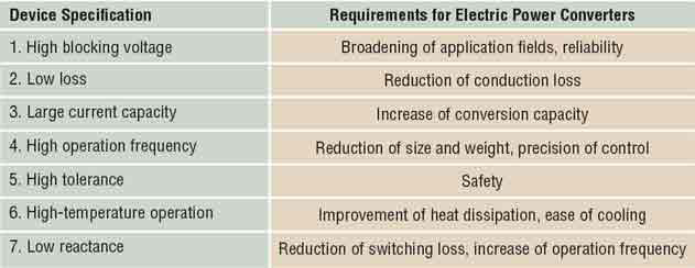
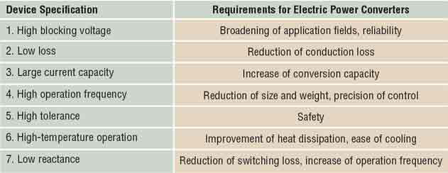
The key components of power electronics are high-power semiconductor devices (transistors and diodes) and electric power converters using these semiconductor devices. In a converter unit, these semiconductor power devices are used as an electrical rectifier or switch, and various electricity specifications (voltage, frequency) are controlled by their complex operation together with passive elements such as capacitors.Reference Zacharias1 Thus, arbitrary electric power wave forms are generated. Low-loss characteristics, high-speed switching capability, and high-blocking voltage capability of the semiconductor power devices are essential factors in the electric power conversion function. The requirements for semiconductor power devices are summarized in Table I from the viewpoint of electric power converter performance.
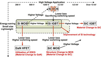
When thinking about future technological innovations for semiconductor power devices, two approaches can be assumed. One improves convenience of use and is typically represented by low-loss characteristics and miniaturization of electric power equipment. The other expands application fields of power electronics represented by the breakdown voltage extension (Figure 1). Si power devices originated as bipolar junction transistors (BJTs); they were then developed into the metal oxide semiconductor field-effect transistor (MOSFET) with improvements for usage convenience through its voltage-controlled feature; and then developed into the gate turn-off thyristor (GTO) and the insulated gate bipolar transistor (IGBT) with expansion to the higher blocking voltage region. Although some performance improvements may be achieved henceforth, major improvements are regarded as difficult because of the materials property limits. There will thus be a limit for future applications for Si-based power electronics. Thus, an R&D approach using wide-gap semiconductors such as SiC or GaN has attracted much attention. In Si-IGBT, which is a bipolar device, the conduction modulation effect by hole injection is utilized in order to reduce ON-resistance and maintain high-blocking voltage capability. Therefore, switching speed is sacrificed in inverter applications compared with the Si-MOSFET, which is a unipolar device. A wide-gap semiconductor power device realizes high-blocking voltage/low ON-resistance/high switching speed performance using MOSFET, junction field-effect transistor (JFET), and heterojunction field-effect transistor (HFET) structures, owing to a high breakdown electric field and saturated drift velocity. When thinking about the status of wide-gap semiconductors from the viewpoint of Figure 1, GaN-HFETs and SiC-MOSFETs will replace Si-MOSFETs and Si-IGBTs, respectively, in terms of high-speed switching, low loss characteristics. Also, SiC-IGBTs correspond to the applications field expansion (high-blocking voltage) of Si-IGBTs.
Corresponding relations between power switching device specifications and requirements for electric power converters from power electronics application systems.
Next-generation power electronics research and development evolution into two directions. One is the direction of high voltage application, the other is energy-saving/small size/lightweight. Red arrows indicate future evolutionary paths, and their meanings are written in red letters. Note: IGBT, insulated gate bipolar transistor; MOS, metal oxide semiconductor; HFET, heterojunction field-effect transistor; SiC, silicon carbide; 2DEG, two-dimensional electron gas.

Technological aspects of next-generation power electronics and related R&D roadmap
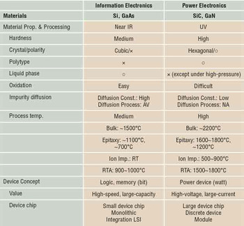
In next-generation power electronics using wide-gap semiconductors, the concept for device development is quite different from the information electronics field where conventional semiconductor materials such as Si and GaAs are used. The differences between these two fields are highlighted in Table II. For information electronics, the focus is on the fabrication of a large number of submicron-size device tips and their integration required from the need of high-speed large-capacity processing. In contrast to information electronics, large-area device tips (several mm2) are required from the specific features of electric power applications for power electronics, while microfabrication technology is necessary for the fabrication of transistor gate structures. In addition, the fabrication processes of SiC wafers and devices are much different from Si technology, especially in process temperature, due to the differences in materials properties.
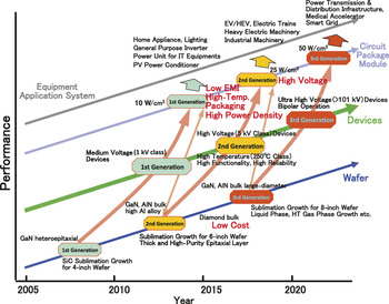
In power electronics, technology developments using SiC and GaN, cooperative development activities across the varied technological domains, such as wafer, device, and circuit/package/module, in addition to the final equipment/application system domain, are essential. In consideration of this situation, an R&D roadmap of wide-gap semiconductor power electronics technology can be derived (see Figure 2).Reference Okumura2 Such a roadmap could be beneficial as a guideline for future technology development. In this roadmap, three different streams across technological domains can be defined as “generations.” These generations can be easily identified by the blocking voltage requirements of the semiconductor power devices, with several technological keywords as shown in the figure, such as “low cost” and “high voltage.”
Comparison between information electronics (Si, GaAs) and power electronics (SiC, GaN).

The comparison is in respect to processing and materials properties, as well as device-centered utility. Note: IR, infrared; UV, ultraviolet; ○, exists; ×, nonexistent; AV, available; NA, not available; RT, room temperature; RTA, rapid thermal anneal; LSI, large-scale integration; Ion Imp. = ion implantation.
Research and development roadmap of wide-gap semiconductor power electronics. The year axis indicates the practical industrialization of each proto-type product. Blue, green, purple, and gray lines express the developments in specific technological domains, such as wafers and devices. Red arrows indicate the third-generation streams. Note: HT, high temperature; EMI, electromagnetic interference; EV, electric vehicle; HEV, hybrid electric vehicle; IT, information technology; PV, photovoltaic.

The first generation is a flow based on 1 kV-class blocking voltage power device technology using four-inch SiC sublimation wafers or GaN/Si wafers, which are already commercially available. Household appliances and lighting, IT server power supplies, and general-purpose inverters are assumed as its primary applications. In this generation, various practical-use electric power converters have been recently demonstrated. As a result, the probability of industrialization of wide-gap semiconductor power electronics has increased; however, uncertainty about wafer size, quality, and supply stability remain concerns from a business point of view.
In such situations, interest in second generation wafer technology has increased. The key phrase for this flow is “price reduction.” The enlargement of the wafer diameter to six inches and improvement of wafer quality, particularly dislocation density, are its primary R&D targets. In addition, the bulk crystal growth of GaN and diamond are included in this generation. The R&D targets of device technology in the second generation are 5 kV-class blocking voltage devices with high-reliability/high-temperature operation capability/high functionality, and the corresponding epitaxial growth technology is thick, high-speed, high-purity epitaxial growth. The assumed application fields are infrastructure/transportation systems such as electric vehicles/hybrid electric vehicles, railroad, and heavy industrial machinery. High-temperature packaging, high power density, and low electromagnetic interference will be the key phrases for this application domain.
The third generation is defined as a more advanced technology development flow. This flow includes the development of eight-inch wafers and the solution growth method aiming at further price reduction for the wafer domain. For the device domain, bipolar devices with a blocking voltage of greater than 10 kV, such as IGBT, are aimed at, where “high voltage” is a key phrase. For the application domain of this generation, the electric power network infrastructure with high functionality, such as the smart grid, or high-voltage medical accelerator power supplies, such as an x-ray generator and a heavy ion accelerator, are assumed as R&D application targets.
For a long time, the technological development level to practical application of wide-gap semiconductor materials, typically represented by SiC, has lagged behind that of conventional semiconductors such as Si and GaAs. This is primarily due to the difficulty in crystal growth and device fabrication. However, remarkable progress has been achieved in recent years in this regard.Reference Okumura2,Reference Okumura3 As a result, first-generation wide bandgap semiconductor power electronics technology is well established, and superior performance of various types of electric power equipment using these first-generation power devices have been demonstrated successively.
In Japan, second- and third-generation technologies for wide bandgap semiconductor materials have been investigated in several national projects. Following these projects, a new R&D scheme, “Cross-Ministerial Strategic Innovation Promotion Program (SIP)/Next-Generation Power Electronics,” has started in Japan.4 Similar R&D schemes concerning power electronics using wide bandgap semiconductors have also launched around the globe, such as “Next-Generation Power Electronics Innovation Institute,”5 “New York Power Electronics Manufacturing Consortium”6 in the United States, and the “Silicon Carbide Power Electronics Technology for Energy Efficient Devices”7 in Europe.
Present status and future prospect of SiC power electronics
The R&D status of wafers, devices, and applications is presented from the viewpoint of the wide bandgap semiconductor power electronics roadmap in Figure 2 and focuses on SiC. Referring to Figure 2, the wafer domain, the devices domain, and the equipment/application domain, including the circuit/package/module, will be explained.
Four-inch SiC wafers are already commercially available. The existence of “micropipe” defects, which are micrometer-sized holes penetrating the wafers, have long been recognized as a critical problem peculiar to SiC;Reference Kimoto and Cooper8 however, this “micropipe” problem has been almost solved. Instead, various dislocations/stacking faults have been recognized as main defects to be solved in the SiC crystal. It is well known that threading screw dislocations cause reverse-bias current leakageReference Tsuji, Tawara, Tanuma, Yonezawa, Iwamuro, Kosaka, Yurimoto, Kobayashi, Matsuhata, Fukuda, Okumura and Arai9,Reference Fujiwara, Katsuno, Ishikawa, Naruoka, Konishi, Endo, Watanabe, Tsuruta, Onda, Adachi, Nagao and Hamada10 and oxide reliability deterioration,Reference Senzaki, Shimozato, Kojima, Kato, Tanaka, Fukuda and Okumura11 and basal plane dislocations cause forward degradation of the p-n junction, which is a phenomenon where the ON-resistance increases under forward-bias operation.Reference Jacobson, Bergman, Hallin, Janzén, Tuomi and Lendenmann12 Commercial SiC wafers typically show a dislocation density of approximately 10,000/cm2 or a little less, and more improvements in dislocation density are expected from the viewpoint of reliability of SiC MOSFETs.
The price reduction of SiC wafers is a big barrier to expanding practical applications of SiC-related technology, and an urgent issue is the realization of six-inch wafers as the second generation wafer technology. This has been recently achieved both in the United States and Japan,Reference Palmour, Das, Ryu, Hull, Zhang, Callanan and Agarwal13,14 and the commercial fabrication of six-inch wafers is expected in the near term. It should be noted that a dislocation density of less than 5000/cmReference Okumura2 for a six-inch wafer has also been reported.Reference Kondo, Takaba, Yamada, Urakami, Okamoto, Kobayashi, Masuda, Gunjishima, Shigeto, Ooya, Sugiyama, Matsuse, Kozawa, Sato, Hirose, Yamauchi and Onda15
At present, the most successful process for growing SiC crystals is the sublimation method, but several concerns have arisen because it is a closed, nonequilibrium system. Thus, solution growth and gas phase growth are being explored for the third-generation technology to pursue low-cost and high-quality growth processes, and a 4H-SiC (four-layered hexagonal SiC) crystal several cm in thickness has been fabricated by solution growth,Reference Daikoku, Kado, Sakamoto, Suzuki, Bessho, Kusunoki, Yashiro, Okada, Moriguchi and Kamei16 which is one of the promising non-sublimation methods. On the other hand, epitaxial growth technology to make a device active layer has gone into the market based on four-inch multi-wafer growth (around 10 wafers) technology, and a uniformity sufficient for practical fabrication has been realized in terms of the film thickness and doping density required for the first generation.
In recent years, it has been identified that surface defects on SiC epitaxial films greatly influence device performance. A reduction in surface defect density is urgently required for the epitaxial growth technology, although uniformity in thickness and doping density is also important. As for second-generation technology, efforts toward high speed (more than 100 μm/h) and thick film growth (several tens or several hundreds of microns thickness)Reference Ishida, Takahashi, Kojima, Okumura, Arai and Yoshida17,Reference Ito, Storasta and Tsuchida18 as well as high-purity growth are in progress aiming at high-blocking voltage devices. In particular, fast epitaxial growth using chloride precursors has attracted attention.Reference La Via, Camarda, Canino, Severino, La Magna, Mauceri, Vecchio and Crippa19 When bipolar operation of power semiconductor devices is pursued, point defect reduction and carrier lifetime improvement of thick epitaxial layers are needed. The carrier lifetime was revealed to be governed by the concentration of the deep level named Z1/2,Reference Danno, Nakamura and Kimoto20 and values more than 10 μs have been realized using ion implantation or oxidation processing to the epilayers.Reference Kimoto, Nanen, Hayashi and Suda21,Reference Miyazawa, Ito and Tsuchida22
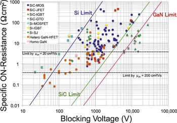
In the device domain, 1 kV-class SiC Schottky barrier diodes have already gone into the market as first-generation technology, and they are implemented in high-end IT server power supplies and home electric appliances. The state of the art of power switching devices is shown in Figure 3 as a relation between specific ON-resistance and blocking voltage. Regarding SiC transistors, technology development aiming at 1 kV/1 mΩcm2-class has been continuously carried out, and blocking voltage/ON-resistance values exceeding those of Si power transistors have been reported, such as 660 V/1.8 mΩcm2 for a planar-type MOS structure,Reference Harada, Kato, Suzuki, Okamoto, Yatsuo, Fukuda and Arai23 790 V/1.7 mΩcm2 for a trench-type MOS structure,Reference Nakano, Mukai, Nakamura, Nakamura and Kamisawa24 and 1000 V/1.5 mΩcm2 for a JFET,Reference Tanaka, Takatsuka, Yatsuo, Arai and Yano25 as a normally-OFF device. Much better characteristics of 700 V/1.01 mΩcm2 for a JFET,Reference Tanaka, Okamoto, Takatsuka, Arai, Yatsuo, Yano and Kasuga26 and 630 V/0.79 mΩcm2 and 1200 V/1.41 mΩcm2 for a trench MOSFETReference Nakamura, Nakano, Aketa, Nakamura, Mitani, Sakairi and Yokotsuji27 have also been reported if the threshold voltage and normally-OFF features are neglected.
State-of-the-art specific ON-resistance and blocking voltage for various power switching devices reported so far. Specific ON-resistances on bipolar structures are differential values. The three straight lines indicate the unipolar limit of each semiconductor material. Specific ON-resistance of actual switching devices is also governed by channel mobility μch, as indicated by dashed lines. It is found that switching device performance by wide bandgap semiconductors has already far surpassed that by Si; however, it has not reached the materials limits yet. Note: SiC, silicon carbide; MOS, metal oxide semiconductor; JFET, junction field-effect transistor; IGBT, insulated gate bipolar transistor; GTO, gate turn-off thyristor; MOSFET, metal oxide semiconductor field-effect transistor; SJ, super junction; HFET, heterojunction field-effect transistor.

Thus, it seems that R&D efforts to improve the blocking voltage/ON-resistance characteristics have completed the first phase for the first generation. Related R&D activity has shifted to improvements in current capacity and reliability for the construction of electric power conversion modules. Instead, the recent R&D trends are expanding to the higher voltage regions. Concerning the second-generation device technology, several fabrication trials have been conducted, as shown by the reports of high-blocking voltage MOSFETs with 3 kV/45 mΩcm2,Reference Peters, Mitlehner, Elpelt, Schörner and Stephani28 4.2 kV/23 mΩcm2.Reference Stum, Bolotnikov, Losee, Matocha, Arthur, Nasadoski, Rao, Saadeh, Stevanovic, Myers-Ward, Deey and Gaskill29 Following these preliminary reports, 5 kV-class large-capacity PiN diodes (p-type/intrinsic/n-type) and a 3.3 kV-class high-blocking voltage MOSFET have recently been developed, aiming at railroad applications. In this case, an ON-resistance of 15 mΩcm2 has been demonstrated.Reference Hamada, Miura, Hino, Kawakami, Imaizumi, Sumitani and Oomori30,Reference Kono, Furukawa, Ariyoshi, Suzuki, Tanaka and Shinohe31
Most recently, 3.3 kV/10 mΩcm2 characteristics have been demonstrated using a trench MOSFET structure.Reference Harada, Kato, Shinozaki, Kobayashi, Ariyoshi, Kojima, Sometani, Senzaki, Tanaka and Okumura32 R&D of a super junction structure using SiC is also in progress, and its blocking capability surpassing a normal structure has already been demonstrated.Reference Kosugi, Sakuma, Kojima, Itoh, Nagata, Yatsuo, Tanaka and Okumura33 The technology development trends in the device/package domains are directed to “higher voltage,” a voltage region of more than 10 kV that is assumed as third-generation technology. In this regime, ON-resistance reduction by conductivity modulation is necessary even for SiC transistors. Bipolar operation devices such as GTO and IGBT become the development targets, different from MOSFETs in the second generation. The first demonstration of SiC IGBT was 12.5 kV/5.3 mΩcm2 for an n-channel structure.Reference Ryu, Cheng, Dhar, Capell, Jonas, Clayton, Donofrio, O’Loughlin, Burk, Agarwal and Palmour34 Interest in electric power transmission and distribution network has increased rapidly, and the development of SiC bipolar devices has attracted more attention as the most advanced technology driver of SiC device technology. As a result, previously mentioned high-quality thick SiC films, BJTs with 20 kV blocking voltage,Reference Miyake, Okuda, Niwa, Kimoto and Suda35 13 kV/6 A SiC-PiN diode,Reference Okamoto, Tanaka, Matsumoto, Mizukami, Ota, Takao, Fukuda and Okumura36 16.5 kV/11 mΩcm2 N-channel SiC-IGBT, and 6.5 kV switching using a 20 A chip (8 mm square)Reference Yonezawa, Mizushima, Takenaka, Fujisawa, Kato, Harada, Tanaka, Okamoto, Sometani, Okamoto, Kumagai, Matsunaga, Deguchi, Arai, Hatakeyama, Makifuchi, Araoka, Oose, Tsutsumi, Yoshikawa, Tatera, Harashima, Sano, Morisaki, Takei, Miyajima, Kimura, Otsuki, Fukuda, Okumura and Kimoto37 have been recently demonstrated.
In the equipment/application domain, practical demonstrations of various electric power equipment have been reported using SiC 1 kV-class low-loss power transistors, including a general-purpose inverter,38 an inverter-implemented motor,39 and a power conditioner for photovoltaic power generation.Reference Matsumoto, Yamada, Kondo, Ikeda and Kimura40 A motor drive and power supply are two types of primary applications of electric power equipment. Superiority of SiC to Si device-based equipment has been demonstrated in terms of efficiency and size/weight, owing to the low-loss characteristics and high-speed switching performance of wide-gap semiconductor devices. Compared with Si, the usage of SiC power devices allows for the output power density one or two orders of magnitude higher as an electric power converter,Reference Simanjorang, Yamaguchi, Ohashi, Nakao, Ninomiya, Abe, Kaga and Fukui41,Reference Sato, Matsui, Zushi, Murakami, Tanimoto, Sato and Yamaguchi42 which is recognized as a large incentive for the actual introduction of SiC-based equipment to various application systems used in society.
Performance improvement of the total system is enabled by adoption of low-loss high-power switching device components, where electric power loss across the application system can be reduced dramatically, and is demonstrated by the installation of SiC hybrid inverters in Tokyo Metro trains.43 Such a demonstration will be a future target for second-/third-generation technology. Corresponding SiC transistors are now under development, while there has been demonstration of a high-speed 5 kV single-phase three-level converter using SiC PiN diodes.Reference Takao, Tanaka, Sung, Wada, Shinohe, Kanai and Ohashi44 For the next stage, several technical issues remain, such as total design technology aiming at high output power density, high-temperature/high-voltage/high-frequency packaging technology, and low electromagnetic interference technology for noise reduction.
Summary
Owing to recent successive breakthroughs in wafer and device technologies, superior characteristics such as a SiC single power device tip surpassing Si power devices have been demonstrated. On the other hand, many challenges remain, especially in the backend process. Such problems cannot be solved by simple extension of conventional Si technology, because the newly revealed problematic aspects of high-temperature, high-speed switching, high-voltage, and large-current capacity are beyond the conventional technology in Si power electronics. Energetic efforts for more advanced technology development are still necessary in the future.
Acknowledgment
The author greatly thanks T. Tanaka for investigating and discussing reported power device characteristics of various kinds of structures.