Introduction
Currently, printed antennas are being used in all communication devices, from pagers to android mobile phones, satellite communications, radars, and aircraft. This massive commercial success has caused rapid advancement in the design and development of these printed antennas. Several structures have been reported for the ultra-wideband (UWB) spectrum by making different slots: curved, rectangular, circular, “L” profile, triangular, semi-circular, and (U)-profile [Reference Azim, Islam and Misran1–Reference Yadav and Baudha6]. By making two rectangular slits in the backplane and cutting curved-shaped slots in the element, bandwidth enhancement is reported [Reference Shagar and Wahidabanu7]. Miniaturized structure by introducing defective ground plane, resulting in lower resonance, is reported [Reference Chakraborty, Rana, Sarkar and Das8]. Fifty percent of miniaturization is reported in “serpentine structure” from the conventional rectangular antenna [Reference Rizvi, Awan and Hussain9]. The partial ground plane by introducing circles in it with a rectangular patch, resulting in the frequency band enhancement is reported [Reference Baudha, Gupta and Yadav10]. UWB spectrum has been reached by making a circular disc-type antenna [Reference Abdelraheem and Abdalla11]. The 3.1–10.6 GHz band for multiple applications by round cutting of rectangular element and cutting a slot in the backplane, as reported [Reference Awad and Abdelazeez12]. By introducing different types of slots in the antenna, resulting in good impedance matching [Reference Baudha, Basak, Manocha and Yadav13]. The stable polar pattern has been achieved by cutting a slot in a rectangular structure [Reference Deshmukh, Singh, Zaveri, Gala and Ray14]. By making a modified patch with the defective backplane and making a unique dumbbell-shaped structure antenna, UWB band applications have been reported [Reference Yadav and Baudha15, Reference Baudha, Yadav and Bansal16]. Increased electrical current path by cutting an arrow-shaped slot in a defective backplane is reported [Reference Hota, Baudha, Mangaraj and Varun Yadav17]. Stable radiation patterns were reported; by cutting a rectangular shape in the backplane and introducing a half-circular disc in the main patch [Reference Sudeep, Goswami and Yadav18, Reference Guo, Wang, Chen and Parini19]. UWB behavior is reported by cutting a circular slot [Reference Ahmed and Sebak20] and using a U-shaped tuning stub and a circular monopole disc as reported in [Reference Kishk and Lee21, Reference Liang, Chiau, Chen and Parini22].
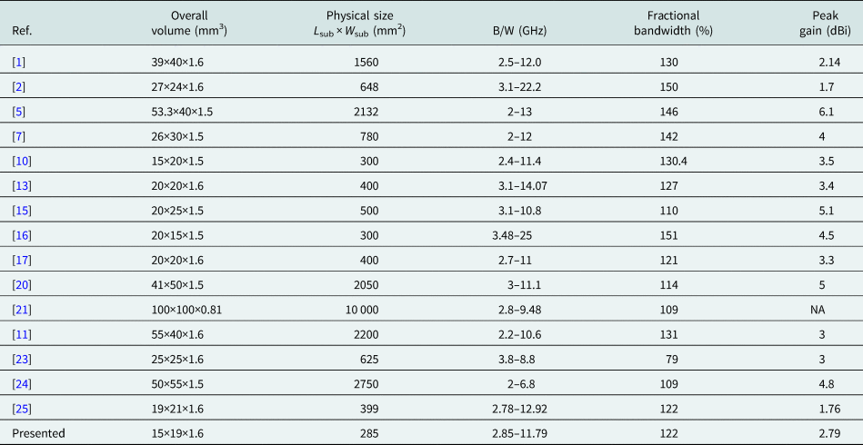
A comparison between recently published articles with presented antenna structure is shown in Table 1. We will also discuss computer-simulated radiation losses, gain, simulated radiation efficiency, radiation pattern at different frequencies in the following sections.
A comparison of the presented antenna with recently published article in references.

Antenna structure and construction
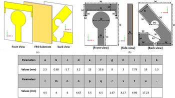
Figure 1 shows the geometric configuration with precise parameters and optimal dimensions of the compact antenna. The substrate used is FR-4 with overall dimensions of 15×19×1.6 cubic millimeters. The design is engraved on FR-4 substrate and is made of annealed copper (Cu) with electrical conductivity of 5.8×10⁷ S/m.
The geometric configuration and the optimum dimension of the proposed antenna with exact parameters (all values are in mm).

The structure's design comprises of a modified patch and rectangular strips in the upper part of the main circular element, which is being fed by a 50 Ω microstrip line. Square and circular slots are also used in the backplane for creating lower frequencies. The antenna's complete length is denoted by “j”, and width is denoted by “e”. “k” represents the substrate's thickness. The design of the patch is of a modified circular type which is evolved from a simple conventional circular patch structure.
To develop a modified circular patch structure, firstly, rectangular parasitic element are added upwards of the front-portion with the size of “e×d” and further two small rectangular strips are attached to both ends of rectangular parasitic with the size of “a×b”. Further development of the design is done by making a defective backplane by adding a rectangular element with the size of “l×u”. This strip is then rotated by 315°. Furthermore, a circular slot is cut inside the rectangular strip with the diameter of “m” and one more square slot of size “r” is cut in the center of the lower backplane. After that, another circular slot with the diameter of “n” is itched out for better resonance in lower frequencies.
This modified design is fed by a 50 Ω line of size “h×i”. It is observed that the presented structure resonates from 2.85 to 11.79 GHz with 122.1% of impedance bandwidth in a very compact overall size of 285 mm2.
Stages of development
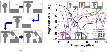
Figure 2 shows the five stages of development and the suggested antenna's return loss (S11). The development was done using simulation on the CST (Computer Simulation tools) microwave studio tool. Stage 01 shows a circular patch and a partial backplane on the antenna. A patch with a diameter of 8 mm is being fed through a microstrip feed line with overall size of (width 3 mm×length 7.79 mm). Here, the length of the partial backplane is 5.5 mm. The width is kept the same as that of a substrate, therefore it is resonating from 4.7 to 8.9 GHz. Stage 02 shows the modification of the front patch. This is done by adding the parasitic rectangular patch of size “15×3.2” mm2 due to which lower frequency shifted and the structure starts resonating from 4.5 GHz. Stage 03 shows the modified main front plane. Two additional rectangular strips are attached at both ends of the parasitic rectangular patch of size “2.5×0.68” mm2. This stage helped to decrease the lower band of the operating frequency range to below 4.25 GHz.
(a) Five stages of development, (b) The return loss (magnitude of S11) of the presented antenna.

Stage 04 shows modifications done in the backplane. The addition of rectangular strips to the backplane further decreases the lower band of the operating frequency range below 3.7 GHz. These strips are connected to the ground plane with a size of “17.23×4.5” mm2. This strip is then rotated by 3150. Furthermore, a circular slot is cut inside the rectangular strip which has the diameter of “4 mm”. Stage 05 is the final stage of development. The development is completed by the introduction of slots in the backplane. One square slot is cut into the backplane of size “1.67×1.67” mm2. There was an additional cut out in the shape of a circular slot with a “6 mm” diameter. These slots in the backplane help to increase the lower and higher bands of the operating range from 2.85 to 11.79 GHz.
Antenna's parameter study
We have performed parameters study to optimize the results by changing the most crucial parameters that could impact the results during the designing process of an antenna. Here in this section, we investigated the variation of three parameters and optimized the simulation results based on their effect on the (S11) parameter results.
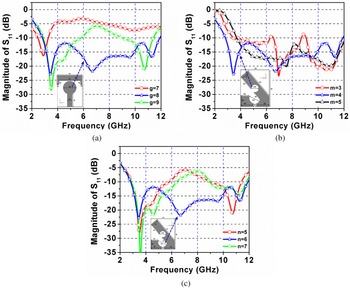
Figure 3 shows the changes in radiation losses of the antenna with variations in different parameters. Figure 3(a) shows the “g” parameters, it is varied from 7 to 9 mm. “g” is the diameter of the main circular element. When “g” is reduced the antenna is not in operating from 3.3 to 12 GHz. The UWB result is obtained when the diameter is kept at an optimum value of 8 mm. Figure 3(b) shows the variation of radiation loss (S11) with variation in “m”, varied from 3 to 5 mm. “m” is the diameter of a slot in the middle of the backplane. Changing the size of the diameter changes the results. When the diameter is small at 3 mm the impedance mismatching takes place between the operating bands. If the diameter is large at 5 mm, the results are better but still not usable throughout the range. The optimized results are obtained at 4 mm. Figure 3(c) shows the variation in “n”. “n” signifies the diameter of the second slot in the lower backplane. It is varied (from 5 to 7) mm by changing the size of the slot, there is variation in the S-parameters. The structure is useful for dual-band only when the size is kept at 5 mm (from 2.85 to 5.8 GHz and 9 to 11.2 GHz). The optimized results are seen at “n = 6 mm”.
Variation in radiation loss (S11) of the antenna with variation in the different parameters. (a) Parameter “g”, (b) Parameter “m”, (c) Parameter “n”.

Results and discussion
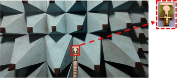
The suggested antenna is a compact, lightweight, and low-cost solution for UWB applications. Figure 4 shows (stage-5) measurement and testing setup in an anechoic chamber with the help of (up to 20 GHz) VNA Analyzer and an anechoic (non-reflective) chamber by connecting the 50 Ω A-type connector.
Shows (stage-5 antenna) measurement and testing setup in an anechoic chamber.

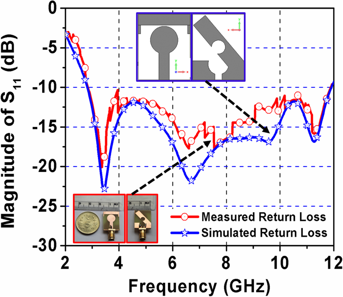
Figure 5 shows the simulated and measured (S11) for an antenna. As indicated by the curve, it is clear that both curves are in good agreement besides minor oscillating variations at the middle frequencies.
Simulated and measured reflection coefficient (S11) for an antenna.

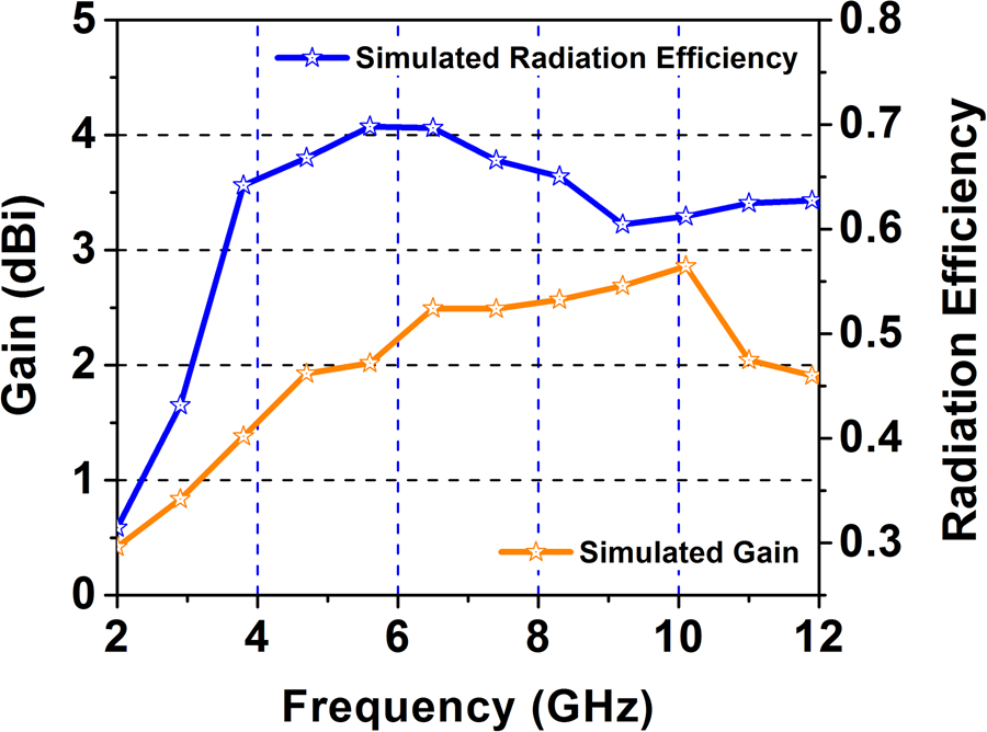
Figure 6 shows the computer-simulated gain and simulated antenna efficiency curve of the suggested antenna which is simulated using the CST tool. It can be observed that the gain steadily increases with the frequency. This shows that the gain is proportional to frequency. The peak gain of 2.79 dBi is observed at 10.2 GHz frequency. The radiation efficiency is very low in the initial frequencies where the antenna has poor return loss, but efficiency increases once the frequencies near the working range. Low radiation efficiency is due to the fact that as the frequency increases ohmic losses also increases. Moreover the substrate used for designing the antenna is Fr4, which is a lossy material. The peak radiation efficiency is observed between 5 and 6.6 GHz with a value of 0.72 or efficiency of 72%. As can be seen in the graph, the radiation efficiency decreases gradually while the frequency increases.
Simulated gain and radiation efficiency of the proposed antenna (stage-05).

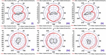
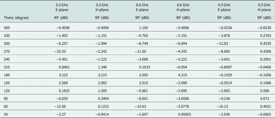
Figure 7 shows the Co-pol, and Cross(X)-Pol. Radiation pattern at different frequencies of the proposed modified antenna. This helps us to understand the direction of radiation of the radiator at a selected frequency. Table 2 shows Radiation plane data at the different degrees (angles). The radiation pattern is shown in 02 planes perpendicular to each other, E Plane (90 degrees, yoz), and the H Plane (0 degrees, xoz). At three frequencies, the antenna is very efficient, and therefore the radiation pattern is stable. The proposed structure has a good steady radiation pattern over the band. Omni-directional and Bi-directional radiation patterns have justified the characteristics of the monopole radiator.
Measured and simulated Co. and Cross polarization (I−II) at 3.4 GHz, E and H-plane, (III−IV) at 6.6 GHz, E and H-plane and (V−VI) at 9.5 GHz E and H-plane.

Radiation plane data at different degrees (angles).

Conclusion
A compact UWB square and circular slot ground plane planar antenna with a modified circular patch for multiple applications has been designed, fabricated, measured, and tested. The proposed modified antenna's physical size is 15×19×1.6 mm3, and its electrical size is 0.18λ 0×0.14λ 0×0.015λ 0. The total fractional bandwidth (S11 <−10 dB) stands at 122.1% in the wide band of 8.94 GHz starting from 2.85 to 11.79 GHz. in a very compact physical size of 285 mm2. The peak gain is around to be 2.79 dBi at 10.2 GHz. The peak radiation efficiency is observed to be 72% between 5 and 6.6 GHz. The suggested compact antenna shows a stable bi-directional and omnidirectional radiation pattern over the entire band. All these properties of the presented antenna are suitable for various applications in UWB. It can also be used for the WiMax band at 3.5/5.5 GHz, WLAN band at 5.2/5.8 GHz, and satellite communication at 4/6 GHz, among other applications.
 Manohar Golait obtained his B.E. degree in electronics engineering from Manoharbhai Patel Institute of Engineering and Technology, Gondia (India) in 2006 and obtained his M.Tech degree in Electronics Engineering from Bapurao Deshmukh College of Engineering, Sewagram (India) in 2016. He has been pursuing his Ph.D. degree from department of Electronics Engineering, G H Raisoni University, Saikheda (India) since 2020. His field of interest are microstrip antenna, microwave engineering.
 Manish Varun Yadav obtained his B.E. degree in electronics and communication engineering from Government Engineering College, Ujjain (India) in 2007 and obtained his M.E. degree in digital communication from Rajiv Gandhi Proudyogiki Vishwavidyalaya, Bhopal (India) in 2011. He has been pursuing his Ph.D. degree from Department of Electrical & Electronics Engineering, Goa Campus, BITS, Pilani, (India) since 2018. His fields of interest are microstrip antenna, planar antenna. He is a Life Member of India Society of Technical Education (ISTE), and member of institute of electrical and electronics engineers (IEEE).
 Dr. Balasaheb H. Patil obtained his Bachelor's degree in electronics & telecommunication engineering from Saitribai Phule Pune University, Pune in year 2001. He obtained M.E. E&TC (Microwave Communication) in year 2010 from Saitribai Phule Pune University, Pune. He obtained Ph.D. E&TC in year 2020 from Saitribai Phule Pune University. His Ph.D. thesis is in the area of Image Inpainting in electronics & telecommunication engineering.
 Dr. Sudeep Baudha is an assistant professor in the Department of Electrical and Electronics Engineering, BITS Pilani, K K Birla Goa Campus, India. He obtained his M.Tech degree in radio frequency and microwave engineering from Indian Institute of Technology, Kharagpur (India) in 2009 and Ph.D. degree from Indian Institute of Information Technology Design and Manufacturing (IIITDM), Jabalpur (India) in 2016. His fields of interest are microstrip antenna, planar antenna, microwave communication etc. He is also associated with several research journals as a reviewer. He is a member of institute of electrical and electronics engineers (IEEE).
 Dr. Lokesh Kumar Bramhane is an assistant professor in the electronics and telecommunication engineering department of G H Raisoni College of Engineering, Nagpur, (India). He obtained his B.E. degree in electronics and telecommunication engineering from the Shri Govindram Seksaria Institute of Technology and Science, Indore, (India) 2007. He obtained his M-Tech degree in VLSI & Embedded System Design from NIT Bhopal in 2012 and Ph.D. degree from PDPM Indian Institute of Information Technology Design and Manufacturing (IIITDM), Jabalpur, (India) in 2017. His field of interests are semiconductor devices, biosensors, IC design, antenna design & fabrication and nanowires.