Introduction
Energy conversion directly from solar energy to chemical bonds is one of the most attractive ways to overcome the global energy crisis.[ Reference Dunn 1 – Reference Rostrup-Nielsen and Rostrup-Nielsen 3 ] Recently, hydrogen (H2) has received tremendous attention as an alternative to fossil fuels owing to its sustainability and minimal environmental impact. In this situation, the photoelectrochemical (PEC) water splitting is a promising approach for the sustainable production of hydrogen as a fuel from the sunlight. Among the various candidate semiconductors for PEC water splitting, p-type silicon (p-Si), which has a narrow bandgap of 1.1 eV can absorb wide range of wavelengths ranging from ultraviolet to near infrared.[ Reference Chen, Shen, Guo and Mao 4 , Reference Osterloh and Parkinson 5 ] It also has cost-efficiency and well-organized photovoltaic technologies. However, the p-Si has high overpotential at the interface of p-Si/electrolyte because of its poor hydrogen evolution reaction (HER) kinetics originating from the high hydrogen adsorption of Gibbs free energy. Furthermore, Si is thermodynamically vulnerable to photoactive dissolution.[ Reference Reece, Hamel, Sung, Jarvi, Esswein, Pijpers and Nocera 6 – Reference Strandwitz, Turner-Evans, Tamboli, Chen, Atwater and Lewis 8 ] To overcome the overpotential issue, the noble metal catalysts such as Pt, Pd, and Rh are generally used for HER catalyst.[ Reference Zhu, Lin, Li, Liao, Lifshitz, Sheng, Lee and Shao 9 – Reference Kye, Shin, Lim, Jang, Oh and Hwang 11 ] Although these catalysts are effective to decrease the overpotential in PEC water splitting of p-Si, the scarcity and high cost of noble metal catalysts are critical challenges to overcome in research of alternative energy system development. Moreover, the most of noble metal catalysts are used in the form of nanoparticles, which are not able to prevent the surface of p-Si photocathode from the photocorrosion. Therefore, it is highly significant to develop the efficient and earth-abundant photocatalysts, which can protect the surface of p-Si, to replace the noble metal catalysts.
Recently, two-dimensional transition metal disulfides (2D TMDs) such as molybdenum disulfide (MoS2) and tungsten disulfide (WS2) are one of the promising candidates for replacing noble metal catalysts due to their inherently high surface-to-volume ratios and the large number of catalytically active edge sites for HER.[ Reference Andoshe, Jeon, Kim and Jang 12 – Reference Ding, Meng, English, Cabán-Acevedo, Shearer, Liang, Daniel, Hamers and Jin 15 ] These materials are generally synthesized by exfoliation, solution-based method, and chemical vapor deposition (CVD). Even though the TMD nanoparticles synthesized by exfoliation or solution-based method have a lot of electrochemically active edge sites, it is difficult to obtain a uniform and dense thin film to cover the entire surface of p-Si. We used the CVD synthesis technique to overcome these limitations by synthesizing the homogeneous thin films, which can protect the surface of p-Si. The synthesis of MoS2 and WS2 by using CVD techniques are mainly subdivided into three methods; (i) thermolysis of solution precursors, (ii) sulfurization of metal oxide thin films, and (iii) vapor deposition of the powder precursors (sulfur and metal chlorides).[ Reference Ding, Song, Xu and Jin 16 – Reference Bianco, Losurdo, Giangregorio, Sacchetti, Prete, Lovergine, Caperzzuto and Bruno 18 ] In the vapor deposition of powder precursors, it is difficult to make the uniform TMD thin films and thus the whole surface of a p-Si photocathode cannot be passivated by the TMD thin film. The MoS2 thin film catalysts, which were grown by simple thermolysis method have been reported that it can provide the relatively high photocurrent density and the lower overpotential compared with p-Si. Furthermore, it can be durably operated over 50 h without any notable degradation.[ Reference Kwon, Choi, Hong, Moon, Shim, Kim, Kim, Sohn, Jeon, Lee, Nam, Han, Kim and Jang 19 ] However, the WS2 thin film, which is analogue of MoS2 cannot be obtained by this method because of the coordination of ammonium tetrathiotungstate ((NH4)2WS4) with any solvent is poor to make uniform precursor layers.[ Reference Panigrahi and Pathak 20 ] In this regard, the sulfurization of a WO3 thin film is considered as the most favorable way to obtain uniform WS2 thin film, which act as the HER catalyst and passivation layer for p-Si photocathode. Although the sulfurization of WO3 thin films have been demonstrated,[ Reference Fu, Wang, Yang, Huang, Zhang and Xiang 21 , Reference Lan, Li and Liu 22 ] the application of the WS2 thin film catalysts for the p-Si photocathode has not been reported to the best of our knowledge.
Here, we demonstrate that the WS2 thin film catalysts synthesized by the simple sulfurization of WO3 thin films can provide the low overpotential (0.18 V at 1 mA/cm2) and high photocurrent density (8.37 mA/cm2 at 0 V) via heterostructuring with p-Si photocathode. By changing the thickness of the WO3 thin films, the thickness of the sulfurized WS2 thin films could be controlled. Although all synthesized WS2 thin film catalysts can improve the overpotential of p-Si, the 23-nm-thick WS2 thin film catalysts (sulfurized from the WO3 10-nm-thick film) shows the best performance among all the samples. The Faradaic efficiency of 23-nm-thick WS2 thin film/p-Si heterojunction photocathode is over 90%. The investigation of charge transport resistance by using electrochemical impedance spectroscopy (EIS) indicates that the 23-nm-thick WS2 thin film catalysts can efficiently transport the photogenerated electrons from p-Si to electrolyte. These results clearly show the promising potential of WS2 thin film catalyst synthesized by simple sulfurization of WO3 thin films in the efficient PEC hydrogen production.
Experimental
SiO2 (300 nm)/Si wafers (1–10 Ω-cm, <100> plane, DASOMRMS Co., Ltd) were cleaned with a standard piranha solution (3:1 volume ratio of H2SO4, 95% grade and H2O2, 30% grade) with conventional cleaning procedures followed by ultrasonication in acetone, isopropyl alcohol, and deionized (DI) water. The DI water was purified by water purification system (Human Power, Human Co., Ltd., Seoul, Republic of Korea, 18.3 MΩ-cm). The tungsten trioxide (WO3, 99.995% purity, Sigma-Aldrich, 204781) thin films with various thicknesses (5, 10, and 20 nm) were deposited by using thermal evaporator (KVE-T2000, Korea Vacuum Tech Co., Ltd., Gimpo, Gyeonggi-do, Republic of Korea,). In order to synthesize the WS2 thin films, we used the simple sulfurization process as following. The N2 and H2 (99.9999%, high-purity) gases were used for the sulfurization process in a thermal CVD system. First, the CVD furnace temperature was raised to 700 °C and was maintained at this temperature for 50 min under flow of H2 and N2 at 1 Torr. The flow rate of H2 and N2 was set at 40 and 200 cm3/min, respectively, by using mass flow controllers (MKS Co., Ltd., Seoul, Republic of Korea, Type 1479A). Then, sublimation of sulfur power (99.998%, Sigma-Aldrich, 213292) precursor was initiated in the other heating zone, whose temperature was set at 300 °C. This process was kept for 1 h for the successful sulfurization of WO3 thin films. Once the sulfurization process was completed, the [poly(methyl methacrylate)] (PMMA, GPC 10000, Sigma-Aldrich, 81497) dissolved in chlorobenzene (99.5% purity, Sigma-Aldrich, 319996) with concentration of 2 g/50 mL was spin-coated onto the CVD-grown thin films. The PMMA/thin films/SiO2/Si substrates were immersed in a buffered oxide etchant to separate the thin films from the substrate by etching away the SiO2 layers. The obtained thin films were washed with DI water seven to nine times to remove the residual etchants and were transferred to the arbitrary substrates. After the PMMA/thin film membranes had perfectly adhered onto the substrates, the PMMA layers were removed using hot acetone bath at 50 °C for 1 h.
The PEC measurements (Ivium Technologies, Eindhoven, Netherlands, Model: Nstat) were carried out with a three-electrode system using a saturated calomel electrode as the reference electrode and a graphite rod as the counter electrode in a 0.5 M H2SO4 standard electrolyte solution. We used a graphite rod counter electrode (WonATech Co., Ltd., Seoul, Republic of Korea) to avoid the deposition of Pt on the working electrode. The three-electrode system was set up inside a quartz vessel, which protected the samples from UV absorption. The conversion equation of potentials versus RHE is expressed as:
 $$\eqalign{E_{{\rm RHE}} & = E_{{\rm SCE}} + E_{{\rm SCE}}^{\rm ^\circ} + 0.059 \times {\rm pH}\;{\rm (}E_{{\rm SCE}}^{\rm ^\circ} \cr & = 0.{\rm 242}\;{\rm versus}\;{\rm SHE)}}$$
where the ESCE is potential of saturated calomel electrode, the E°SCE is potential of the saturated calomel electrode with respect to the standard hydrogen potential (SHE), and the pH is 0.5 M H2SO4 is 0.27. A Xe arc lamp (Abet Technologies, Milford, CT, USA, LS150) was used and calibrated to an output of 100 mW/cm2 (AM 1.5 G condition). A scan rate of 10 mV/s was used for the linear sweep with cathodic direction. The incident-photon-to-current conversion efficiency (ICPE) was measured with a light source and a monochromator (DONGWOO OPTRON, MAC150) and the efficiency was calculated by following equation:
 $$\eqalign{{\rm IPCE}\;{\rm (}\lambda {\rm )} & = EQE\; (\lambda ) \cr & = \displaystyle{{ \vert j_{{\rm ph}}({\rm mA/c}{\rm m}^{\rm 2}) \vert \times 1239.8\; ({\rm V} \times {\rm nm})} \over {P_{{\rm mono}}\;({\rm mW}/{\rm c}{\rm m}^{\rm 2}) \times \lambda \;({\rm nm})}}}$$
where the j ph is photocurrent of the sample, the λ is wavelength, and the P mono is the power of monochromator. The external quantum efficiency was measured with a standard Si photodiode. EIS was conducted by applying a constant potential of 0.27 V versus RHE near the open-circuit potential. The sweeping frequency was varied from 250 kHz to 1 Hz using a 10 mV AC dither.
Results and discussion
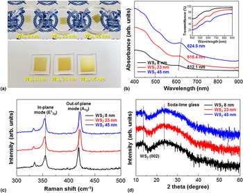
The WS2 thin films used in this study were synthesized by simple sulfurization of WO3 thin films. The WO3 thin films with various thicknesses (5, 10, and 20 nm) were deposited on cleaned SiO2 (300 nm)/Si substrates by using thermal evaporator. To synthesize the WS2 thin films, the simple sulfurization of WO3 thin films was conducted by using thermal CVD system with the sublimation of sulfur power precursors. For the characterization of the synthesized thin films and their application as PEC catalyst, they had to be transferred to substrates such as glass, p-Si, and SiO2/Si wafers. The PMMA was used as the supporting polymer and was spin-coated onto the synthesized thin films for wet transfer. The photographic images of the synthesized thin films floated onto DI water bath and transferred on glass substrates are shown in Fig. 1(a). The yellow color of synthesized WS2 thin films gradually changes to deep as a function of thickness of WO3 precursor thin films. Figure 1(b) shows that the absorbance spectra of WS2 thin films prepared with different thickness of WO3 thin films exhibit similar peak positions for each thin film. The excitonic absorption peaks attributing from the transition of direct gap at the K point of the Brillouin zone. The corresponding peaks are located at the wavelengths of 612, 616, and 624 nm for the 8-, 23-, and 45-nm-thick WS2 thin films, respectively.[ Reference Mishra, Lakshmi and Huang 23 ] The optical absorption peak change originates from the variation of optical band gaps of synthesized thin films. These results are in good agreement with previously reported absorption spectra of the WS2 thin film via other CVD methods.[ Reference Mishra, Lakshmi and Huang 23 ]
Photographic images and characterization of synthesized WS2 thin films. (a) The photographic images of synthesized WS2 thin films floated onto de-ionized water bath and transferred to glass substrates. (b) Absorbance spectra and transmittance of synthesized WS2 thin films. The inset figure shows the transmittance of WS2 thin films. (c) Raman spectra of synthesized WS2 thin films. (d) XRD analysis of synthesized WS2 thin films on glass substrates.

Raman spectroscopy is a general investigation method to detect the atomic vibrations in thin films, especially 2D layered materials. For a WS2 thin film, the in-plane vibration (E1 2g) appears near 355 cm−1, while the out-of-plane vibration (A1g) appears near 418 cm−1.[ Reference Berkdemir, Gutiérrez, Botello-Méndez, Perea-López, Elías, Chia, Wang, Crespi, López-Urías, Charlier, Terrones and Terrones 24 ] The Raman spectra of the synthesized WS2 thin films from sulfurization of WO3 thin films with different thicknesses are shown in Fig. 1(c). The difference in frequencies between those two Raman modes of WS2 thin films depends on the number of layers and can be easily used as a thickness indicator.[ Reference Li, Zhang, Yap, Tay, Edwin, Olivier and Baillargeat 25 ] The frequency difference between E1 2g and A1g modes was approximately 64 cm−1, indicating that the synthesized WS2 thin film is multilayer. The peak gap between E1 2g and Alg gradually increased as a function of increase of WO3 thin films precursor layer thickness. Figure 1(d) shows the x-ray diffraction (XRD) patterns of the WS2 thin films prepared with different WO3 precursor layer thicknesses. Because the XRD measurement of synthesized thin films was conducted on soda-lime glass substrate, the broad peak near 23° was obtained in all the samples. The small peak, which is WS2 (002) plane, near 13° appeared in the synthesized WS2 thin films, regardless of the WO3 precursor layer thicknesses.[ Reference Nguyen, Sohn, Oh, Jang and Kim 26 ]
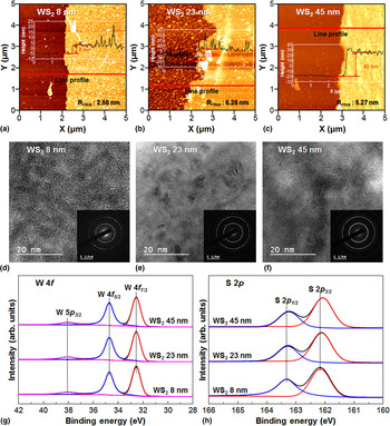
To evaluate the thickness and surface morphology of the synthesized thin films, atomic force microscopy was used as shown in Figs. 2(a)–2(c). The thickness of synthesized WS2 thin films increased from 8 to 45 nm when the thickness of WO3 precursor thin layer increased from 5 to 20 nm. The increase of film thickness in each sample is attributed to the structure modification from 3D monoclinic WO3 (space group of P21/n) to 2D hexagonal WS2 (space group P63/mmc). The weak van der Waals bonds in the WS2 thin films make the films thicker than the original 3D WO3 thin films. All the synthesized thin films were nano-granular. The serrated-surface of the synthesized thin films with different thickness provides a large surface area than the atomically flat surface of a single-crystalline WS2 layer. The root-mean-square (RMS) roughness was 2.6 nm for the 8 nm-thick WS2 thin films fabricated with the sulfurization from 5 nm-thick WO3 film. The RMS roughness increased from 2.6 to 6.2 nm. These increased RMS roughness values could help enhancing the catalytic activity due to the increase of surface area of synthesized 23 nm-thick WS2 thin films. Figures 2(d)–2(f) shows the high-resolution transmission electron microscopy images of synthesized WS2 thin films. The periodic atomic arrangements of the WS2 thin films are obtained and the selected area electron diffraction (SAED) patterns reveal a hexagonal structure with poly-crystalline. Furthermore, the pin-hole free WS2 thin films, which can protect the dissolution of p-Si photocathode were successfully synthesized by using simple sulfurization method. These results indicate that the poly-crystalline WS2 thin films were synthesized by sulfurization of WO3 films. In order to investigate the chemical components and atomic ratios of the synthesized thin films, the x-ray photoemission spectroscopy (XPS) was conducted as shown in Figs. 2(g) and 2(h). For the WS2 thin films with different thicknesses, the atomic ratio of W to S was constant at 65% to 35%, regardless of the WO3 precursor thicknesses. Five peaks appear at 32.4, 34.6, 38, 162, and 163.3 eV in the synthesized WS2 thin films, which are assigned to W 4f 7/2, W 4f 5/2, W 5p 3/2, S 2p 3/2, and S 2p 1/2, respectively. These results are well-consistent with the findings of previous reports on WS2 crystals.[ Reference Xu, Zhang, Lin, Zheng, Zhong, Xia, Li, Sophia, Fuhrer, Cheng and Bao 27 ]
(a)–(c) Atomic force microscopy images of synthesized WS2 thin films by using sulfurization of different thickness of WO3 thin films. (d)–(f) High-resolution transmission electron microscopy images of synthesized WS2 thin films. The SAED pattern shows that the synthesized thin films were poly-crystalline. (g)–(h) The core level x-ray photoemission spectroscopy (W 4f and S 2p) analysis of synthesized WS2 thin films.

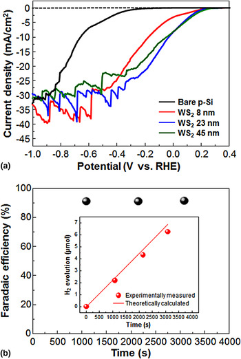
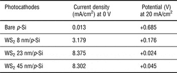
The PEC measurement of the WS2/p-Si heterostructure photocathodes was conducted using a 3-electrode cell with 0.5 M sulfuric acid (H2SO4) as the HER electrolyte.[ Reference Nguyen, Choi, Jeon, Kwon, Jang and Kim 28 ] We employed a saturated-calomel electrode as reference electrode and a graphite rod as counter electrode. Figure 3(a) displays linear-sweep voltammetry (LSV) measurements under a solar simulated light source (air mass 1.5 G). The dashed lines show the result of LSV measurement without light. We set the potential when the photocurrent density reaches −1 mA/cm2 as the onset potential. The large negative onset potential of −0.35 V was observed for the bare p-Si photocathode. As mentioned in introduction, the bare p-Si requires an additional overpotential due to the carrier concentration and kinetics issue.[ Reference Reece, Hamel, Sung, Jarvi, Esswein, Pijpers and Nocera 6 – Reference Strandwitz, Turner-Evans, Tamboli, Chen, Atwater and Lewis 8 ] The 23-nm-thick WS2/p-Si photocathode exhibited the lowest onset potential of 0.2 V. For the 23-nm-thick WS2/p-Si photocathode, the anodic shift of the onset potential was 0.63 V with regard to that of the bare p-Si. The PEC performances with photocurrent density at 0 V and potential at 20 mA/cm2 were summarized in Table I. It is well-known that the edges of 2D TMD materials could act as catalytic active sites. The nano-serrated surface of the synthesized WS2 thin films as displayed in Figs. 2(a)–2(c) should contain a number of active sites. The RMS roughness values of the 23- and 45-nm-thick WS2 thin film shows the higher value (6.3 and 5.3 nm) than that of 8-nm-thick WS2 thin film (2.6 nm), indicating that the thicker WS2 thin films have the plenty of catalytic edge sites and a large surface area. For this reason, the photocurrent densities of the 23- and 45-nm-thick WS2/p-Si photocathodes at 0 V (versus reversible hydrogen electrode (RHE)) showed the higher values of 8.3 and 8.2 mA/cm2 than that of the 8-nm-thick WS2/p-Si photocathode (3.2 mA/cm2). Meanwhile, the saturation photocurrent density of the 45-nm-thick WS2 thin film/p-Si photocathode is lower than the other photocathodes due to its lower transmittance, as shown in the inset of Fig. 1(b). These results obviously display that the PEC performances of the WS2/p-Si photocathodes rely on the thickness of the WS2 thin film and that an optimum WS2 thin-film thickness exists.
Photoelectrochemical hydrogen evolution reaction performances of the WS2 thin films on p-type Si photocathodes with different thickness. (a) Linear-sweep voltammetry curves of WS2 thin film catalysts/p-Si heterojunction photocathodes. (b) Faradaic efficiency measurements for the 23-nm-thick WS2/p-Si photocathode under illumination at 0 V versus RHE with 0.5 M H2SO4 electrolyte. The inset graph shows the amount of H2 evolved as a function of the calculated amount of H2 by the passed charge.

The summarized PEC performances of WS2/p-Si heterojunction photocathodes.

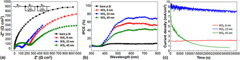
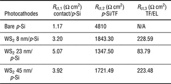
To elucidate the Faradaic efficiency for H2 evolution of the WS2 23 nm/p-Si photocathode, we conducted gas chromatography measurements at constant voltage of 0 V versus RHE under continuous illumination. The H2 evolution was monitored several times at intervals of 15 ~ 20 min. The inset graph of Fig. 3(b) displays the relation between the amount of evolved H2 and the calculated amount of H2 by the passed charge. Although the straight line does not exactly fit into the data point, but the Faradaic efficiency represents over 90% [Fig. 3(b)], which suggests that most of the measured current goes toward H2 evolution. Figure 4(a) shows Nyquist plots of the EIS. The charge transfer resistances (R ct) could be determined using a simplified equivalent circuit. The low R ct at each interface appears in the small semicircular arc in the Nyquist plot. The semicircular arcs, which correspond to R ct were considerably reduced as the thickness of WS2 thin films increased from 8 to 23 nm. This decrease in the semicircular arc was affected by the enhancement of the thin film quality with the increase of WS2 thin film thickness. The 23-nm-thick WS2/p-Si photocathode exhibited the smallest R ct value that is smaller than one order of magnitude compared with the other WS2/p-Si photocathodes, as displayed in Table II. We evaluated the incident-photon-to-current conversion efficiency spectra of the WS2/p-Si photocathodes at 0 V versus RHE as illustrated in Fig. 4(b). Among the WS2/p-Si photocathodes, the highest efficiency over 60% was obtained by the 45-nm-thick WS2/p-Si photocathode at long wavelengths (660–730 nm). This phenomenon originates from a decrease in the band gap of the WS2 thin film as the thickness of the WS2 thin film becomes thicker. Meanwhile, the areas under the IPCE curve of 23- and 45-nm-thick WS2/p-Si photocathodes are almost similar, in accordance with the similar photocurrent densities at an applied bias of 0 V versus RHE.
Investigation of photoelectrochemical hydrogen evolution reaction performances for the synthesized WS2 thin films/p-Si heterojunction photocathodes. (a) Electrochemical impedance spectroscopy analysis of fabricated WS2/p-Si photocathodes. (b) Incident-photon-to-current-efficiency curves of fabricated WS2/p-Si photocathodes. (c) Chronoamperometric curves of 8-, 23-, and 45-nm-thick WS2 thin films/p-Si photocathodes for 10 h. The 23-nm-thick WS2 can maintain the 83% of initial photocurrent density even after 10 h.

The summarized charge transport resistance values of various thicknesses WS2/p-Si photocathodes.

TF, thin film; EL, electrolyte; p-Si/electrolyte.
We investigated the long-term stability of the WS2/p-Si photocathodes using chronoamperometric measurements as shown in Fig. 4(c), to examine whether our WS2 thin film catalysts could carry out a role as a passivation layer of p-Si. For the 23-nm-thick WS2 thin film, the degradation of the photocurrent density at 0 V versus RHE was significantly suppressed, maintaining 83% of initial current for 10 h. Even though the 8-nm-thick WS2 thin film catalyst shows the lowest catalytic activity among the three samples, the initial photocurrent density can be maintained at 0 V versus RHE over 10 h due to the relatively strong adhesion between the p-Si and its bottom layer. On the other hand, the severe photocurrent degradation can be observed in the 45-nm-thick WS2 thin film catalyst. To check the surface morphologies of the as-transferred and the chronoamperometry measured samples, field-emission scanning electron microscopy was conducted for 8-, 23-, and 45-nm-thick WS2 thin film catalysts, as shown in Fig. S1. For the as-transferred samples, the clean and flat surface without pin-holes was observed. However, the surface of the 45-nm-thick WS2 thin film was significantly damaged by the catalytic reaction, while the 8- and 23-nm-thick WS2 thin films maintained the flat surface without pin-holes. This result is attributed to the fact that the thicker 2D material has the weaker van der Waals force in its top layers. In this reason, the top layers of the 45-nm-thick WS2 thin film could be easily exfoliated or damaged by the catalytic reaction.
Conclusions
We have demonstrated that the WS2 thin film HER catalyst synthesized by simple sulfurization of WO3 thin film for efficient PEC water splitting. The synthesized WS2 thin film successfully transferred using the simple method to the target substrate. Thickness dependent PEC performance of WS2 thin films was studied. The 23-nm-thick WS2/p-Si heterojunction photocathodes showed excellent photocurrent density of 8.3 mA/cm2 at 0 V with 72% of incident photon-to-current conversion efficiency. The onset potential of bare p-Si is shifted from −0.35 to 0.2 V due to WS2 thin film HER catalyst. The WS2/p-Si photocathode can be stable for a longer time in the liquid electrolyte while generating hydrogen. The WS2 thin film HER catalysts could be one of the promising candidates for reducing the overpotential of bare p-Si as well as for protecting from photo-electrochemical corrosion.
Supplementary material
The supplementary material for this article can be found at https://doi.org/10.1557/mrc.2017.37.
Acknowledgments
This work was supported by Samsung Research Funding Center of Samsung Electronics. Ki Chang Kwon acknowledges the Global Ph. D Fellowship Program of the National Research Foundation of Korea funded by the Ministry of Education.