Introduction
Polymer solar cells (PSCs) based on conjugated polymer and fullerene composites offer special opportunities for capturing solar energy in view of the potential for fabrication over large area flexible substrates [Reference Jensen, Mikkelsen and Krebs1] by means of low cost, roll-to-roll solution processing [Reference Krebs, Gevorgyan and Alstrup2, Reference Krebs3]. The power conversion efficiency (PCE) of PSCs has reached up to 17% based on “tandem cell architecture,” emphasizing the prospects for PSCs [Reference Krebs4, Reference Dennler, Scharber and Brabec5, Reference Li, Zhu and Yang6, Reference Meng, Zhang, Wan, Li, Zhang, Wang, Ke, Xiao, Ding, Xia, Yip, Cao and Chen7, Reference Li, Gao, Wan, Zhang, Kan, Xia, Liu, Yang, Feng, Ni, Wang, Peng, Zhang, Liang, Yip, Peng, Cao and Chen8]. PSCs make use of a nanometer-sized bicontinuous network of the polymer and fullerene, commonly referred to as a bulk heterojunction (BHJ) [Reference Shaheen, Brabec, Sariciftci, Padinger, Fromherz and Hummelen9]. The nanostructure facilities dissociation of the exciton, and the bicontinuity of the network provides pathways for the transportation of electrons and holes to their corresponding electrodes [Reference Ma, Yang, Gong, Lee and Heeger10].
In a tandem cell, a multilayer structure equivalent to two or more photovoltaic cells is used in series or in parallel [Reference Shrotriya, Wu, Li, Yao and Yang11]. The multijunction cells in series mode offer potential to improve efficiency and the open-circuit potential (V oc) to values close to the sum of the V oc values of each individual cell. A recent fabrication of a tenfold-stacked tandem device with a high V oc (5.89 V) emphasizes the great potential for charging energy storage devices [Reference Zou, Deng, Potscavage, Hirade, Zheng and Adachi12] using PSCs. Whereas for the devices in a parallel mode, the short-circuit current density (J sc) equals the sum of the J sc values of each subcell [Reference Dennler, Scharber, Ameri, Denk, Forberich, Waldauf and Brabec13]. Conventional inorganic tandem cells focus on using two semiconductors with different band gaps leading to absorption over a broad range of photon energies within the solar emission spectrum because of their complementary absorption spectra [Reference Dou, You, Yang, Chen, He, Murase, Moriarty, Emery, Li and Yang14]. Typically, a high band gap (BG) semiconductor for the front cell and a low BG semiconductor for the back cell are used. The order of the stacked layer, i.e., a high BG followed by a low BG polymer [Reference Dou, You, Yang, Chen, He, Murase, Moriarty, Emery, Li and Yang14, Reference Gevaerts, Furlan, Wienk, Turbiez and Janssen15, Reference Minnaert and Veelaert16, Reference Chou, Kwan, Hong, Chen and Yang17, Reference Dou, Gao, Richard, You, Chen, Cha, He, Li and Yang18], is based on the fact that the electron–hole pairs generated by photons with energies greater than that of the energy gap of the photoactive materials rapidly relax to the respective band edges. However, this design principle may not necessarily hold up for PSCs. In view of the low mobility of the charge carriers in the polymer–fullerene composites, an increase in the thicknesses of the active and intermediate layers increases the internal resistance of the device and can adversely affect both the V oc and the fill factor (FF) [Reference Shrotriya, Wu, Li, Yao and Yang11]. As a result of the low thickness of the films, the front cell in the tandem structure can have low optical absorption that allows a large portion of the optical flux through to reach the back cell [Reference Kim, Lee, Coates, Moses, Nguyen, Dante and Heeger19]. As a result, PSCs fabricated using the same or reverse order BG semiconductors for the front and back cells can be explored to improve V oc as well as efficiency. There are limited examples of tandem cells with a stacking order of a low BG polymer followed by a high BG one in the literature [Reference Kim, Lee, Coates, Moses, Nguyen, Dante and Heeger19, Reference Namkoong, Boland, Lee and Dean20]. Although the tandem cell may have a higher optical density over a wider fraction of the solar spectrum than that of a single cell, it may suffer from an increased internal resistance in arising from the intermediate layers that separate the stacked cells [Reference Chou, Kwan, Hong, Chen and Yang17]. Tandem devices based on two identical layers of PCDTBT:PC71BM separated by a ZnO/Au/MoO3 intermediate layer with a PCE of >4% have been reported recently [Reference Puetz, Steiner, Mescher, Reinhard, Christ, Kutsarov, Kalt, Lemmer and Colsmann21], which demonstrates a new method of designing tandem devices.
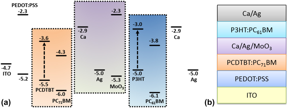
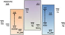
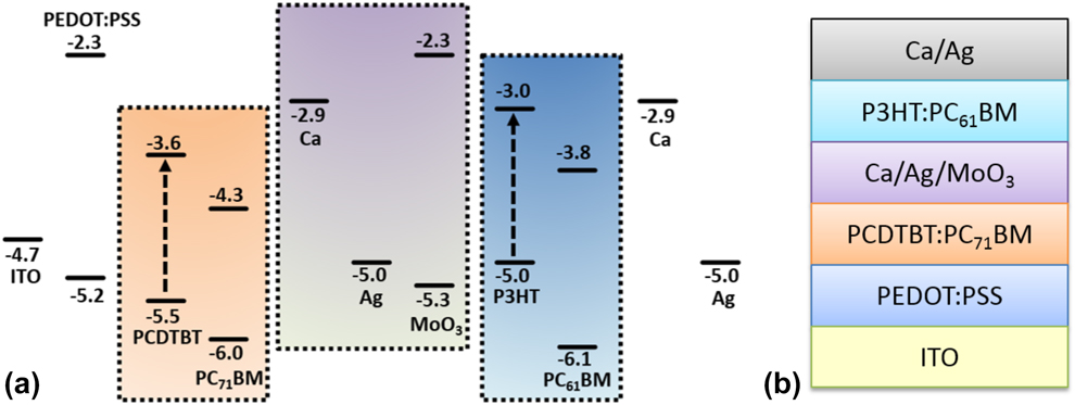
In this work, the concept of using a low BG polymer–fullerene composite as the front cell in a tandem structure is investigated. A semiconducting polymer, poly[N-9′-heptadecanyl-2,7-carbazole-alt-5,5-(4′,7′-di-2-thienyl-2′,1′,3′-benzothiadiazole)] (PCDTBT) [Reference Blouin, Michaud, Gendron, Wakim, Blair, Neagu-Plesu, Belletete, Durocher, Tao and Leclerc22], is a medium BG polymer with the highest occupied molecular orbital (HOMO) and lowest unoccupied molecular orbital (LUMO) energy levels of −5.4 and −3.6 eV, respectively [Reference Park, Roy, Beaupre, Cho, Coates, Moon, Moses, Leclerc, Lee and Heeger23]. For the front cell, we used a blend of PCDTBT and a modified fullerene, [Reference Li, Zhu and Yang6,Reference Li, Zhu and Yang6]-phenyl C71-butyric acid methyl ester (PC71BM), a BHJ with an internal quantum efficiency approaching 100% [Reference Park, Roy, Beaupre, Cho, Coates, Moon, Moses, Leclerc, Lee and Heeger23]. The optical density of this blend in form of a thin film is between 10 and 20% depending on the wavelength [Reference Chu, Alem, Verly, Wakim, Lu, Tao, Beaupre, Leclerc, Belanger, Desilets, Rodman, Waller and Gaudiana24]. Thus, the structure allows 70–80% of the incoming solar energy to be transmitted to the second subcell. Two tandem structures were fabricated using either PCDTBT:PC71BM composite (T1) or the high BG polymer poly(3-hexylthiophene) (P3HT) and [Reference Li, Zhu and Yang6,Reference Li, Zhu and Yang6]-phenyl-C61-butyric acid methyl ester (PC61BM) composite (T2) as the back cell. PCEs of 3.4% and 1.6% were achieved for T1 and T2 devices, respectively. The device structure and the alignment of HOMO and LUMO energy levels for a T2-type device are schematically depicted in Fig. 1. The effect of interlayer properties on the performance of the devices are studied. By altering the thickness of the interlayer materials, up to 50% changing in PCE is observed for both tandem structures. In addition, the observed V oc values increased close to the sum of the V oc of the two individual subcells, demonstrating the successful use of low and high BG PSCs as the front and back cell, respectively. The solar energy, transmitted through the front cell, has enough intensity to generate power to its full potential in the back cell [Reference Kim, Lee, Coates, Moses, Nguyen, Dante and Heeger19]. A minor voltage loss (0.1–0.2 V) is generally attributed to the interface-dominated recombination [Reference Gunawan, Todorov and Mitzi25].
The energy level alignment (a) and device structure (b) in a tandem solar cell using PCDTBT:PC71BM (1:5) and P3HT:PC61BM (1:1) as the front and back BHJ layers, respectively.
Results and discussion
Optical property
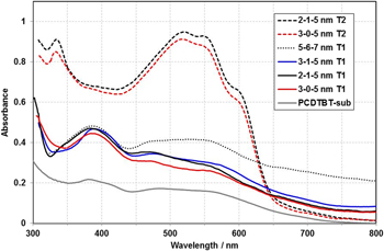
The absorption spectra of the two types of tandem devices T1 (front cell, PCDTBT:PC71BM; back cell, PCDTBT:PC71BM) and T2 (front cell, PCDTBT:PC71BM; back cell, P3HT:PC61BM) are shown in Fig. 2. These devices were fabricated using BHJ of polymer–fullerene photoactive blends having different thicknesses of Ca, Ag, and MoO3 as the intermediate layers. Absorption spectra of PCDTBT (with two maxima at 398 and 578 nm) and PC71BM (at 378 and 478 nm) are superimposed in the 1:5 blend films displaying three bands at ∼380, 480, and 570 nm in the spectra of T1 devices. The absorption spectra of T2 devices, on the other hand, provide evidence of extensive π–π stacking of the polythiophene backbone and the formation of an ordered structure for P3HT, as indicated by absorption peaks at ∼520, 550, and 600 nm while the peak at 330 nm is due to PC61BM. The absorption feature of the T2 devices mainly resembles that of the P3HT:PC61BM thin film because of its intense absorbance in the visible range and the fact that a P3HT:PC61BM film (150 nm) [Reference Li, Yao, Yang, Shrotriya, Yang and Yang26] is generally thicker than PCDTBT:PC71BM one (70 nm) [Reference Beiley, Hoke, Noriega, Dacuna, Burkhard, Bartelt, Salleo, Toney and McGehee27, Reference Namkoong, Kong, Samson, Hwang and Lee28].
Absorption spectra of tandem devices T1 (front cell, PCDTBT:PC71BM; back cell, PCDTBT:PC71BM) and T2 (front cell, PCDTBT:PC71BM; back cell, P3HT:PC61BM). The intermediate layer thicknesses vary, Ca = 2–5, Ag = 0–6, and MoO3 = 5–7 nm, abbreviated as 2-1-5 nm etc. for each sample. Also shown is the spectrum of a PCDTBT:PC71BM subcell.
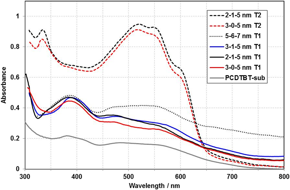
Judging by the flat absorption at around 800 nm, it is evident that increasing the total thickness of Ca, Ag, and MoO3 in the intermediate layer causes a reduction in the intensity of transmitted light that reaches the back cell. Therefore, the best PV performance was observed for T1 and T2 devices with an intermediate layer having a combined thickness of less than 10 nm. Namely, the optimized thicknesses are Ca = 2–3, Ag = 1, and MoO3 = 5 nm (abbreviated as 2-1-5 or 3-1-5 nm in Fig. 2).
Thin film morphology
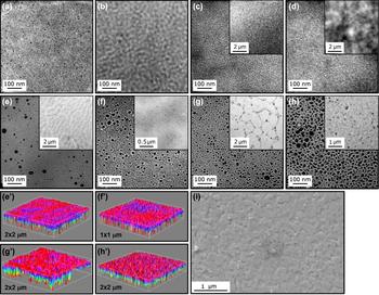
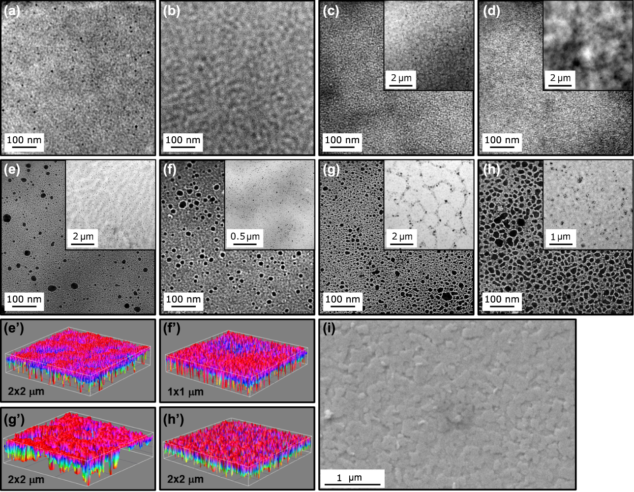
The transmission electron microscopic (TEM) and scanning electron microscopic (SEM) images of the thin films are shown in Fig. 3. A clearly defined nanoscale phase separation with feature sizes of 10–20 nm is observed in Figs. 3(a)–3(d), which is comparable to the diffusion length of photogenerated excitons ensuring an efficient exciton dissociation and charge separation at BHJ interfaces. The darker regions in these TEM images are attributed to the phase-separated PCBM domains with a higher electron density than the polymer ones. When a very thin interfacial layer of Ca, Ag, and MoO3 is deposited between the photoactive layers, it generates nanometer-sized islands on the thin film. Increasing the thicknesses of deposited metals results in a higher density of islands. When an extra layer of Ag is inserted between Ca and MoO3, the deposited MoO3 moiety is more likely to attach to Ag-covered Ca islands than to directly deposit on Ca due to the higher surface energy of Ag (γAg = 1.25 J/m2, γCa = 0.50 J/m2). Ag, as a highly diffractive heavy element, is clearly observed [Figs. 3(e)–3(h)]. The existence of Ag helps to form MoO3/Ag/Ca stacks instead of randomly distributed MoO3 and Ca islands. The deposited MoO3 forms a connected network of larger particles on a scale of several hundreds of nm [Figs. 3(e)–3(h) insets and 3(i)]. The intermediate layer also shows improved optical transparency (Fig. 2) and electronic property (see below) with the Ag layer. Based on reconstructed 3D images [Figs. 3(e′)–3(h′)] and the SEM image of a 7-nm MoO3 layer deposited on indium tin oxide (ITO) [Fig. 3(i)], it is confirmed that these islands are part of a network developed in between the front and back cells. Thereby, electrons from the front cell can be recombined with the holes from the back cell at the intermediate layer leading to a combined V oc.
Transmission electron microscope (TEM) images of (a) PCDTBT:PC71BM (1:5 w%), (b) P3HT:PC61BM (1:1 w%), and tandem devices (with Ca–Ag–MoO3 thicknesses in nm) (c) T1: 3-0-5, (d) T2: 3-0-5, (e) T1: 2-1-5, (f) T1: 3-1-5, (g) T1: 3-3-5, and (h) T2: 5-6-7, and 3D images (e′) to (h′) reconstructed from TEM images (e) to (h), respectively, and (i) scanning electron microscope (SEM) image of a 7-nm MoO3 layer deposited on ITO.
Photovoltaic property
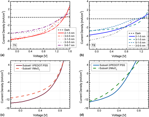
Figure 4 shows the comparison of the JV characteristics of the T1 and T2 tandem cells having different combinations of intermediate layers and device structures of ITO/PEDOT:PSS/PCDTBT:PC71BM//PCDTBT:PC71BM/Ca/Ag and ITO/PEDOT:PSS/PCDTBT:PC71BM//P3HT:PC61BM/Ca/Ag, respectively, whereby // denotes the intermediate layer. The extracted PV parameters are summarized in Table I. The V oc for the cell with Ca/MoO3 intermediate layer (T1: 3-0–5 nm) approaches 1.45 V. However, both T1 and T2 tandem cells with Ca/MoO3 exhibit a convex J–V curve. A similar observation has been previously attributed to a high barrier for charge injection at two interfaces [Reference Uhrich, Schueppel, Petrich, Pfeiffer, Leo, Brier, Kilickiran and Baeuerle29], resulting in carriers to pile up at both sides of the intermediate layer. A Schottky-type contact is thus formed due to the quasi-Fermi level mismatch between Ca (−2.8 eV) and MoO3 (−5.5 eV). For these tandem cells, incorporation of an ultrathin Ag is necessary to suppress the barrier. The Ca/Ag/MoO3 intermediate layer will therefore have a better electronic property than the Ca/MoO3 layer for these PV tandem cells. The disappearance of the convex curve is an indication that the Schottky barrier is overcome by the insertion of Ag (with a work function of −4.7 eV), thus forming Ohmic contacts for effective charge recombination. A higher FF was observed as a consequence of efficient charge recombination at the Ca/Ag/MoO3. Indeed, the insertion of 1 nm Ag between Ca and MoO3 increases the FF of tandem cells from 0.37 (T1: 3-0-5 nm) to 0.45 (T1: 2-1-5 nm) and 0.48 (T1: 3-1-5 nm). The improvement in FF can be attributed to the barrier-free transport of charges between the intermediate and photoactive layers. Additionally, the V oc of the T1 and T2 tandem cells (∼1.4 and ∼1.2 V) with Ca/MoO3 is lower than the summation of the V oc of two subcells. With an ultrathin Ag incorporated between Ca and MoO3, an Ohmic contact between both subcells is fully established, leading to a more efficient charge extraction/recombination. Hence, the V oc of 1.47 and 1.25 V is obtained for the T1 and T2 tandem cells, respectively. Increasing the Ca thickness to 5 nm, while keeping the Ag at 1 nm, generates the convex JV curve once again. It is expected that an ultrathin Ag coating could not effectively cover the larger islands of Ca in these devices.
Current–voltage (JV) characteristics of (a) T1 and (b) T2 tandem devices with a structure of ITO/PEDOT:PSS/PCDTBT:PC71BM//PCDTBT:PC71BM/Ca/Ag and ITO/PEDOT:PSS/PCDTBT:PC71BM//P3HT:PC61BM/Ca/Ag, respectively, under 100 mW/cm2 (AM1.5G) where // denotes the intermediate layer Ca/Ag/MoO3. (c) and (d) The subcells of T1 and T2, PCDTBT:PC71BM (subcell 1) and P3HT:PC61BM (subcell 2), on two types of hole-collecting layers. The intermediate layer thicknesses abbreviated as in Fig. 2.
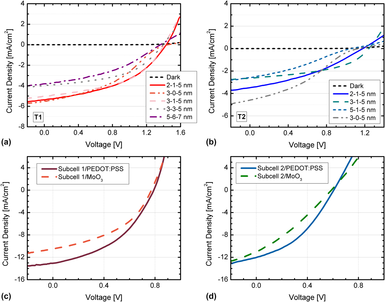
Extracted parameters, short current density (J sc), open-circuit voltage (V oc), FF, and power conversion efficiency (PCE) for T1 and T2 tandem devices and their subcells. The calculated J sc is based on the overlap integral between EQE and AM1.5G spectrum in the range of 330–800 nm.

As shown in Fig. 4, for the T1 devices, the V oc values of the separately prepared front and back subcells are 0.79 and 0.77 V, respectively. For T2 devices, the individual subcells show V oc of 0.79 and 0.58 V. In the best performing devices (T1: 2-1-5 nm and T2: 3-1-5 nm), the V oc values are reaching 94 and 91% of the sum of the subcell V oc. This proves that the two subcells have been successfully connected in series resulting in PCEs of 3.4% and 1.6%, for T1 and T2 tandem cells, respectively. The close match between the observed V oc and the sum of individual cells is a proof of the concept that in a tandem device structure an order of a low BG polymer followed by a high BG polymer can be implemented if the front cell exhibits a low level of optical density allowing a sufficient flux of photons to reach the back cell.
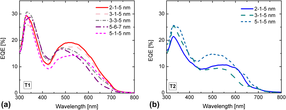
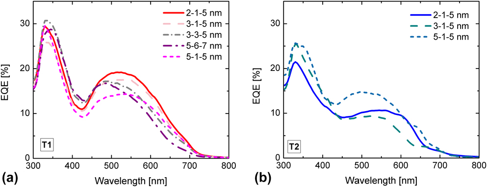
The external quantum efficiency (EQE) of the tandem devices is shown in Fig. 5. For all of these devices, a reasonable photoresponse within the range of 300–730 nm is observed with EQE reaching a maximum value of 0.2 and 0.15 at 500–550 nm for T1 and T2 devices, respectively. As it is seen in Fig. 5, the EQE follows the trend observed in the JV characterization, i.e., the highest EQE belongs to tandem devices with an optimized intermediate layer thickness; Ca = 2–3, Ag = 1, and MoO3 = 5 nm. The tandem devices with a thicker intermediate layer might suffer from reduced incident power but, most importantly, because of a low charge transition/recombination across the intermediate layer (see below), an increase in the thicknesses of this layer increases the internal resistance of the device. As a result, a low current density is generated in these tandem devices compared to their subcells (see  $J_{{\rm{sc}}}^{{\rm{calc}}{\rm{.}}}$ in Table I). Optimization of the intermediate layer composition and optimization of its thicknesses are two important parameters in developing high-efficiency PSC tandem devices.
EQE of (a) T1 and (b) T2 tandem devices with varying intermediate layer Ca/Ag/MoO3 thickness as abbreviated in Fig. 2.
Charge transition across the intermediate layer
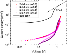
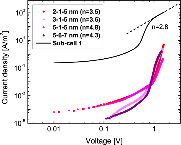
To evaluate the effectiveness of charge transfer across the intermediate layer, the dark current density of all the tandem devices was compared. Figure 6 shows the variation of the dark current density (J) with applied voltage (V) for T1 tandem devices. A striking feature is that J value decreases in devices with a thicker intermediate layer (total thickness of Ca/Ag/MoO3). T1 tandem devices, when compared to their single layer subcell, showed three to four orders of magnitude reduction in J, an indication that the tandem devices are much poorer charge conductors than the single layer devices. In the case of a single-layer device, a modified space-charge limiting current (SCLC) model was adopted to extract the hole mobility μhole based on SCLC equation,
 $$J = {9 \over 8}{\varepsilon _0}\varepsilon {{{V^2}} \over {{L^3}}}{\mu _{{\rm{hole}}}}\quad ,$$
where ε is the relative permittivity of the medium, ε0 is the permittivity of vacuum, and L is the active layer thickness [Reference Chiguvare, Parisi and Dyakonov30]. The extracted hole mobility of PCDTBT (μhole = 3.6 × 10⁻⁵ cm2/V s) is approximately one order of magnitude smaller than values commonly reported for P3HT (μhole = 2.0 × 10⁻⁴ cm2/V s) [Reference Mihailetchi, Xie, de Boer, Koster and Blom31]. The effective ideality factors of the devices are calculated to be in the range of 2.8–4.8 as shown in Fig. 6, which is consistent with the reported experimental and simulation results [Reference Zhao, Li, Yao, Zhang, Zhang, Yang and Hou32, Reference Islam33, Reference Li, Arumugam, Krishnan, Charlton and Beeby34]. The high ideality factor indicates high recombination rate within the BHJ layer. The minority carriers may recombine before moving to the electrodes, because of the low carrier mobility. By involving the tandem structure, the charge carriers transport through more layers before reaching the electrodes and experience higher possibility of recombination at each interface, leading to lower current densities. The orientation of the polymer molecules may change when different interlayer materials are used at the interface, which can bring a significant impact in charge transport efficiency [Reference Ran, Roland, Love, Savikhin, Takacs, Fu, Li, Coropceanu, Liu, Brédas, Bazan, Toney, Neher and Nguyen35]. One possible reason for the superiority of PCDTBT over P3HT-based PV devices is its thinner photoactive layer that results in improved optoelectronic property and PV performance, and that is not the case for T1 and T2 tandem devices.
Thickness dependence of dark current density (J) to the applied voltage (V) for T1 tandem devices. The intermediate layer thicknesses abbreviated as in Fig. 2. The dashed line is a fit to the region with a quadratic variation of J–V for the subcell 1; the extracted hole mobility is 3.6 × 10⁻⁵ cm2/V s. Effective ideality factor n of each device is shown in the plot.
Conclusions
Tandem PSCs using low BG polymers as the front cell and the same or high BG polymers as back cells were successfully fabricated. The effect of intermediate layers was investigated. With the incorporation of an ultrathin Ag layer, Ca/Ag/MoO3 stacks were established vertically, and a connected network of Ca/Ag/MoO3 islands was obtained horizontally. Hence, the electron transport layer of the front cell and the hole transport layer of the back cell are able to overcome the energy barrier and form effective charge recombination centers, leading to a higher FF. The thickness of the Ag layer is essential for maximum coverage on Ca and minimum increase in internal series resistance and light absorption of its own. Fully optimized devices demonstrate a V oc reaching the sum of V oc of the two subcells. J sc of both types of tandem cells were relatively low due to the internal series resistance brought by both of the intermediate layers and the active polymer layers. The power conversion efficiencies of 3.4% and 1.6% for T1 (homotandem cells) and T2 (heterotandem cells) were achieved.
Methods
ITO-coated glass substrates with the sheet resistance of 20 Ω/sqr were patterned and thoroughly cleaned before device fabrication. A 25-nm layer of poly(3,4-ethylenedioxythiophene) poly(styrenesulfonate) (PEDOT:PSS; Clevios P VP AI 4083, Heraeus, Hanau, Germany) was spin coated at 5000 rpm on ITO and baked at 140 °C for 15 min in an ambient atmosphere. The PEDOT:PSS-coated substrates were then transferred into a glove box system.
The front cell BHJ films were deposited from blends of PCDTBT (Luminescence Technology, Taiwan, China) and PC71BM (>99%, Solaris Chem Inc., St-Lazare, Qubec, Canada) in a mixture of 1,2-dichlorobenzene (DCB; 99%, Sigma-Aldrich, St. Louis, Missouri) and chlorobenzene (CB; 99%, Sigma-Aldrich, St. Louis, Missouri) with a 3:1 vol% ratio. The polymer blend was prepared by dissolving 4 and 20 mg of the PCDTBT and PC71BM powder, respectively, in 1 mL of solvents mixture in the glove box (O2 and H2O levels <0.1 ppm) and then stirred at 40 °C for 1 h before use. The polymer ink was spin cast on PEDOT:PSS/ITO substrates at a multistep spin rates of 2500 and 3000 rpm for 6 and 2 s, respectively, with an initial ramping up of 3 s (from 0 to 2500 rpm). The films were placed in a Petri dish (100 × 15 mm) and preheated at 70 °C and carpeted with a filter paper. A portion of 0.5 mL of chloroform was added to the filter paper and the dish was covered for 30 s for each batch of devices to control the solvent vapor [Reference Gholamkhass and Servati36]. Intermediate layers of Ca (2–5 nm), Ag (0–6 nm), and MoO3 (5–7 nm) in this sequence were thermally evaporated (at a vacuum level of 2 × 10⁻⁸ torr) on the PCDTBT:PC71BM layer. For T1 devices, a second layer of PCDTBT:PC71BM was then spin-cast on the metal intermediate layers with the same parameters as the first layer. For T2 devices, however, the back BHJ films were deposited from a 1:1 solution of PC61BM and P3HT (regioregularity 95%, Solaris Chem Inc., St-Lazare, Qubec, Canada) in 1,2-dichlorobenzene (1,2-DCB; 99%, Sigma-Aldrich, St. Louis, Missouri), filtered through a 0.45 µm polytetrafluoroethylene (PTFE) membrane filter (Pall Co., Port Washington, New York) before mixing. The blend ink was spin-cast on the intermediate layer with sequential rates of 250 rpm (3 s), 1000 rpm (15 s), and 1500 rpm (3 s). The films were placed in a covered Petri dish immediately after coating to control the solvent evaporation rate (drying time: 10–20 min). Finally, Ca (20 nm) and Ag (120 nm) were thermally evaporated through a shadow mask to complete the device. The overlapped area of the top and bottom electrodes define an active device area of 0.2 cm2.
Current–voltage (J–V) measurements were conducted on a computer-controlled Keithley 2400 Source Meter (Tektronix, Beaveton, Oregon) whereas the samples were kept in a home-built vacuum sample holder with the transparent front window after transferring out of the glove box. A xenon lamp (150 W, Newport Co., Irvine, California) equipped with an AM1.5G filter was used as the light source. The optical power was 100 mW/cm2, calibrated using a broadband power meter (Newport Co., Irvine, California). The external quantum efficiency (EQE) was measured using monochromatic light from a monochromator (Cornerstone 130, Newport Co., Irvine, California) and the incident power was measured using a power/energy meter (Newport Co., Irvine, California). Bright-field transmission electron microscopic (TEM), scanning electron microscopic (SEM), and atomic force microscope (AFM) images were recorded using Hitachi 8100 (Hitachi High-technologies, Krefeld, Germany), Zeiss Sigma (Zeiss, Oberkochen, Germany) FE-SEM, and Asylum Research MFP 3D (Oxford Instruments, Abingdon, England), respectively. Film thicknesses were measured with a Bruker DektakXT profilometer (Bruker Co., Billerica, Massachusetts). For the purpose of TEM analysis, the devices were immersed in water to enable the polymer films to be peeled off. The floating films were picked up using 500 mesh TEM copper grids. Absorption spectra were measured using a Varian Cary 5000 spectrophotometer (Agilent Co., Santa Clara, California).
Acknowledgments
This work was supported by the Natural Sciences and Engineering Research Council and Canada Foundation for Innovation.