Introduction
Atom probe tomography (APT) is one of the highest performance microscopies yet devised. A three-dimensional, atomic-scale image is produced with single-atom sensitivity, where each atom (actually each isotope) in the image is identifiable. APT is used to study all types of inorganic materials and is gradually demonstrating capabilities for analysis of organic materials. Increasingly, these qualities make APT an essential tool for any modern materials characterization laboratory.
There has been a dramatic improvement in atom probe instrumentation in the past decade that has been driven by the availability of vastly superior commercial instruments, most notably the local-electrode atom probe (LEAP). The atom probe was invented in 1967 at Pennsylvania State University by Müller, Panitz, and McLaneReference Müller, Panitz and McLane1 as a one-dimensional analytical instrument that collected hundreds of atoms per day in 1 nm fields of view. There was only depth registry of atom positions in the data, no lateral positioning information, and the data collection required minutes per atom. By 1973, the origins of tomographic analysis were present in Panitz’s 10 cm atom probe.Reference Panitz2 The first revolution came when a true three-dimensional imaging instrument was developed by Cerezo, Godfrey, and SmithReference Cerezo, Godfrey and Smith3 that could record hundreds of atoms per minute in up to ∼15 nm wide fields of view. We consider the LEAPReference Kelly, Camus, Larson, Holzman and Bajikar4 and related instruments such as the scanning atom probeReference Nishikawa and Kimoto5 combined with focused ion beam (FIB)-based specimen preparationReference Larson, Foord, Petford-Long, Liew, Blamire, Cerezo and Smith6 to be the second revolution in the development of the atom probe. With a LEAP, millions of atoms per minute can be collected with 200 nm wide fields of view with high mass resolution (1/1500, full width at half maximum) on many types of materials.
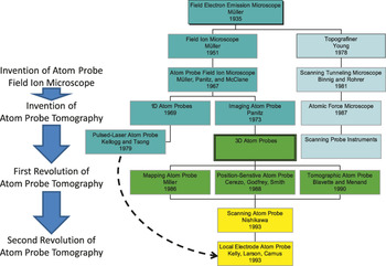
It is helpful to review the history of APT so that one can understand what the LEAP is and how it evolved from its predecessors. This article is intended to be historical in nature and focuses on the people and machines that have led to the current generation of atom probe instruments. In Figure 1, a flowchart of predecessor instruments in the lineage of the modern atom probe is presented. The history will be recounted below with reference to this chart.
Ancestry of the local-electrode atom probe.

Ancestry of the local-electrode atom probe
APT is the name of the technique. There are many types of instruments that may be one-dimensional atom probes (1DAP) or three-dimensional atom probes (3DAP). Some instruments that are 3DAPs were given names such as the position-sensitive atom probe (PoSAP)Reference Cerezo, Godfrey and Smith3 and tomographic atom probe (TAP).Reference Bostel, Blavette, Menand and Sarrau7 Instruments that feature a local electrode, which is a counter electrode for the specimen that produces higher electric fields at a given voltage simply due to its proximity, are LEAPs.
Early history and the field electron emission microscope (∼1935)
One can start a review of the history of APT in the late 19th century. The electron was discovered by J.J. ThomsonReference Thomson8 in 1897, and RutherfordReference Rutherford9 and BohrReference Bohr10 developed the modern view of the structure of the atom in 1913. W.H. Bragg and W.L. BraggReference Bragg11 deduced the atomic nature of materials and packing of atoms in crystals through x-ray diffraction in 1913. Charged-particle quantum optics theory was developed in the late 1920s, and Fowler and NordheimReference Fowler and Nordheim12 predicted the magnitude of the electric field required to strip an electron from an atom. Physicists of the day could fairly readily show that fields of about 109 volts per meter (1 V/nm) should suffice.
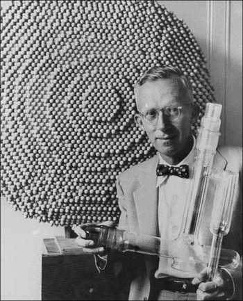
A question one could ask is, “How could one create such a field to form a beam of emitted electrons from a material?” If you consider a set of parallel plates, the electric field in the region between the plates is simply the voltage between them divided by their separation. To get to 109 volts per meter, 10,000 voltsFootnote * across a micrometer separation would suffice. This is not, however, a realistic practical scenario because real electrodes with such a small separation would suffer dielectric breakdown at voltages much lower than this, and the field could never be reached. Physicists certainly understood that then. However, it was known that with a spherical geometry for one of the electrodes, the field on the sphere will vary as the voltage divided by the radius of the sphere. So for 10,000 volts, it is necessary only to make the radius small enough. If the sphere (hemisphere) is on the end of a needle, you get almost the same result. Thus for 10,000 volts, a tip apex radius on the needle of about 1 micrometer will create these fields of 109 volts per meter and cause emission of electrons from the surface. This is a field emission electron source. This brings us to about the end of the 1920s, and Gustav Hertz at the Technical University of Berlin hired Erwin W. Müller as a student to build a field electron emission microscope (FEEM), where they demonstrated this effect and then studied the related phenomenon. Müller, Figure 2, eventually became the father of this scientific discipline of high-(electric) field nanoscience. Incidentally, at the same institute at the same time, Max Knoll had a student, Ernst Ruska, working on a new instrument called an electron microscope.
Photograph of Erwin W. Müller (1911–1977)—father of high-(electric) field nanoscience. Figure courtesy of J.A. Panitz, The University of New Mexico, Department of Physics and Astronomy.

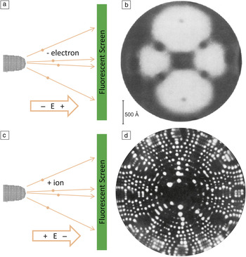
Müller developed the FEEMReference Müller13 around 1935. By creating a field electron emission source and projecting the emission pattern of electrons onto a fluorescent screen, Figure 3a, an image such as that in Figure 3b is formed. This was very exciting in the 1940s when this work was starting to mature, and researchers started to ponder how far the spatial resolution of this technique could be pushed. Could we see atoms? By the mid-1940s, it was clear that the answer was no. The FEEM achieves about two nanometer resolution at best, and it was not going to improve significantly. But this work spurred some thinking that led to the next development—the field ion microscope (FIM).
(a) Schematic of the field electron emission microscope (FEEM). (b) FEEM image of <110> tungsten.Reference Müller14 The twofold symmetry of this pattern is evident. (c) Schematic of the field ion microscope (FIM). (d) FIM image of <110> tungsten.Reference Müller17, Reference Müller18 The first images of atoms obtained by humans were made on October 11, 1955 by Bahadur and Müller.

Field ion microscope: The first images of atoms (1955)
At some point, scientists working with the FEEM wanted to know what would happen if the polarity were reversed. Instead of pulling negative charge out of the tip, could positive charge be removed? At some level, the researchers were thinking they would just clean the specimen to produce a more uniform surface with this approach: reverse polarity to get rid of adsorbed hydrogen on the specimen, then return to electron emission. Instead, they found a steady emitted stream of positive ions, and they could see a field ion emission pattern on a fluorescent screen.Reference Müller14 Higher fields of 1010 volts per meter were required, so needles needed a 0.1 micrometer diameter apex for FIM, Figure 3c. These FIMs produced images of higher spatial resolution than the FEEM. The first high-quality FIM images were produced in 1951 by Müller et al.,Reference Müller15 but they did not achieve atomic resolution. It was not until October 11, 1955 (see Melmed’s account of these eventsReference Melmed16), that Bahadur with MüllerReference Müller17, Reference Müller18 resolved individual atoms with the FIM, Figure 3d, which was the first time humans saw atoms, some 2400 years after Leucippus and Democritus postulated their existence. The word atom is a Greek word for “not divisible.”
Atom probe field ion microscope (1967)
The next development was part of a logical progression. If you were to look at images of atoms over the course of half a dozen years, you may start to ask, “Couldn’t we find a way to figure out the identity of any or all of those atoms?” To accomplish this, Barofsky and MüllerReference Barofsky and Müller19 first attempted using a magnetic-sector mass spectrometer instrument, but eventually Barofsky became convinced that time-of-flight measurements were the better approach.Reference Panitz20 Müller, Panitz, and McLaneReference Müller, Panitz and McLane1 thus settled on measuring time of flight as the way to identify ions.Reference Müller18 This approach required a pulsed field-evaporation event so that atoms begin their flight at a well-defined instant, and the flight time can be determined when the atoms hit the detector. Panitz (a PhD student working with Müller), McLane, and Fowler (technicians in Müller’s lab) were responsible for building this instrument under Müller’s supervision. It was called the atom-probe field ion microscope (APFIM). It was a one-dimensional instrument. The operator would press a button that would send a voltage pulse to the specimen. The oscilloscope screen would show a trace when the detector was hit. This instrument could collect tens of atoms per hour, it had about a 1 nanometer field of view, and its mass resolving power was just sufficient to resolve 56Fe+ from 57Fe+. Panitz recorded the oscilloscope trace on Polaroid-type 57 film, typically exposing a half dozen traces per sheet to save film. A sine wave from a crystal oscillator was recorded on the same sheet of film as a time reference independent of the oscilloscope’s time-base generator. Panitz then projected each film positive 10 × using an Aero Ecktar lens. For each ion, he measured the distance from a reference object with a meter stick and converted that distance on the sine wave to a flight time. By morning, he would have a list of about 100 atoms that he recorded overnight.
The technique progressed quickly as groups at the University of Pittsburgh under Sid Brenner and at the University of Oxford under George Smith began developing atom probes. Groups at Chalmers (Hans-Olof Andrén) and Cornell (David Seidman) started computerizing control of the instrument. Soon, commercial instruments by Vacuum Generators (the APFIM 100 in 1980) and Applied Microscopy (the APFIM 200 in 1986) appeared and offered data collection rates of 100,000 atoms in a day and mass resolving power of 1 part in 2000 with voltage pulsing using a PoschenriederReference Poschenrieder21 lens or a reflectronReference Mamyrin, Karataev, Shmikk and Zagulin22 optic, respectively. These were 1D instruments with a probe hole for the atoms to pass through and a 1 nanometer field of view.
Finally, Russell Young, a student from Müller’s lab, later developed the topographinerReference Young, Ward and Scire23 at NIST using the high-field techniques he learned in Müller’s lab. Young labored on the topographiner for a dozen years into the late 1970s. Building on this concept, Binnig and RohrerReference Binnig and Rohrer24 developed the scanning tunneling microscope in 1981, which led to them winning the Nobel Prize with Ruska in 1986. That spawned atomic force microscopes and then a whole chain of other scanning probe microscopes. Thus, there is a connection between scanning probe microscopy and Müller’s laboratory. Due to the multiple, disparate applications of these devices, it has been suggested that they be called, generally, a Müller tipFootnote †, in honor of the inventor.
The advent of atom probe tomography
The 3D atom probe was a natural progression from the 1D atom probe, yet it was a revolutionary departure from the atom-probe field ion microscope when it was first pursued. Panitz developed what he called the imaging atom probe (IAP)Reference Panitz2 in 1972. It was a short flight path instrument with a full field of view: a design that we shall see later still exists because of its fundamental merit. He could measure time of flight to anywhere on the full detector because it used spherical microchannel plate amplifiers centered on the specimen so that the distance to the channel plate amplifier was the same in all directions. The IAP would record the hit positions of a single atom (or isotope) type at a time from any given voltage pulse by time gating the channel plates. With this approach, an iron map in steel may be recorded, for example. Subsequently, a carbon map could be recorded, and so on. The IAP collected 3D data by manually examining a series of 2D maps of a single preselected species as a function of depth. Since the field desorption process is destructive, only a single species could be examined, unlike a modern 3DAP where a 2D map of all species can be obtained as a function of depth and displayed on a computer screen. Nonetheless, the IAP produced tomographic data from an atom probe, and Panitz should be credited with a significant inventive step in the development of APT.
PoSAP and the first revolution in atom probe tomography
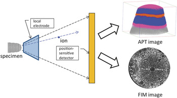
The advent of a true 3DAP that recorded all atom species occurred in the 1980s when position-sensitive detector concepts were adapted to what essentially amounted to IAP-like instruments. Miller (Oak Ridge National Laboratory) conceived of such an instrument and presented his concepts in the mid-1980s.Reference Miller25, Reference Miller26 The first fully operational 3D atom probe was developed in 1988 at the University of Oxford by Cerezo, Godfrey, and Smith and was dubbed the PoSAP.Reference Cerezo, Godfrey and Smith3 It was essentially the schematic in Figure 4 but without the local electrode. One of the authors (Kelly) attended a presentation at the 1988 MRS Fall Meeting in Boston by George Smith, at which time some of the very first data were shown. Cerezo, Godfrey, and SmithReference Panitz2 adapted a wedge-and-strip detector, which has been used in astronomy to a commercial Vacuum Generators APFIM 100 that was in the lab. By adding a 2D detector to a 1D atom probe, they created a working 3D atom probe. The images obtained were spectacular. They contained about one million atoms and showed precipitates and interfaces in materials. As an analytical electron microscopist, Kelly fully appreciated how challenging it would be to do similar work on an electron microscope. This was the first revolution in APT.
Schematic of a short-flight-path atom probe with a local electrode. The detector would be placed close to the specimen to maximize solid angle. If the detector is also capable of modest energy discrimination, then the atom probe (labeled APT) image data may be separated from field ions and a separate field ion microscope (labeled FIM) image may be simultaneously recorded.

Electron-beam-pulsed atom probe
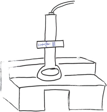
The PoSAP was an extremely successful instrument, as it ushered in a new era in microscopy, but it had its limitations. It took days to collect an image, and it had a ∼15 nanometer field of view. The data collection rate of these instruments was limited by high voltage pulsers available at that time, which could not go to high repetition rates at high voltages. These limitations are what drove us to try to go to much higher repetition rates with the following approach. If we could heat very small volumes quickly, we would have both rapid heating and cooling. Since it was not feasible to focus lasers to submicron spots in an atom probe, this led us to the concept of an electron-beam-pulsed atom probe.Reference Kelly, Mancini, McCarthy and Zreiba27, Reference Kelly, Zreiba, Howell and Bradley28 Focusing electron beams to small diameters (∼200 nm) is possible, so enough energy (∼100 nJ) was delivered in a short enough time (∼100 ps) in a small enough volume (∼106 nm3) that we could achieve high repetition rates with high mass resolution. Thus Larson did his PhD thesis on electron-beam pulsing as another way to get high repetition rates.Reference Larson, Camus and Kelly29 We built an atom probe inside a scanning electron microscope (SEM) and called it the atom probe microscope. This instrument was never successful at demonstrating electron-beam pulsing, but it did suggest that there was a lot of value in having an electron image of an atom probe specimen, and we see this theme returning today. With all of this thinking about electron beam and atom probes, the idea of putting an atom probe inside of a transmission electron microscope (TEM) was a natural next step. Figure 5 is a cartoon that Kelly showed at the 1990 International Field Emission Symposium meeting in a talk about electron-beam-pulsed atom probes. Maybe it was a little bit of wishful thinking, or science fiction, but the merit of putting an atom probe into a TEM is again being pursued (see text later).
A sketch of an electron-beam pulsed atom probe inside the objective lens of a transmission electron microscope. From the 1990 International Field Emission Symposium meeting, Albuquerque, NM. The electron beam would be used for both thermal pulsing and for imaging the tip.

LEAP and the second revolution in atom probe tomography
The next step in the development of the atom probe, and the advent of the second revolution, is the scanning atom probeReference Nishikawa and Kimoto30 invented by Osamu Nishikawa (who also came from Müller’s lab) in 1993. The idea was to have a funnel-shaped electrode and scan it around close to a surface. If there are any sharp points in the area as the aperture passes over, ions will start evaporating through the aperture. The geometry enables a radically different approach to making specimens. Specimens had always been needle shaped, and now Nishikawa was suggesting microtip arrays. This concept had a major impact on how one could think about specimens and instruments.
At this time, we were still trying to address the basic conundrum of the 3DAP; it was a spectacularly successful analytical tool, but it was too slow to be practical. The scanning atom probe started us thinking: Field electron emitter arrays were being developed that had field enhancement factors of up to 10 or more due to proximal electrodes.Reference Spindt, Brodie, Humphrey and Westerberg31 This was key to making a higher data collection rate. If we could lower the voltage, we could go to much higher repetition rates. This all came together in two key thoughts: (1) we could use a local electrode to attain these high data collection rates and not require an electron beam, and (2) we could realize a relative reduction in the energy spread (due to the voltage reduction) and achieve high mass resolution over the entire field of view.Reference Kelly, Camus, Larson, Holzman and Bajikar32 So a local-electrode geometry, like that in Figure 4, mitigated or solved the three biggest issues with the atom probe of the day: (1) specimen geometry (thanks to Nishikawa), (2) data collection rate, and (3) mass resolution for a large field of view. The local-electrode geometry allowed us to go from a 15-nanometer field of view to a 150-nanometer field of view. The speed of the instrument went from about 104 atoms per hour all the way up to 108 atoms per hour. The analytical sensitivity improved from 100 parts per million to 1 part per million. The analyzed volumes increased by 3 orders of magnitude. The mass resolving power has also improved by a factor of 5 to one part in 1500 (due also to other effects such as laser pulsing and reflectron compensators). Instead of working with 10-millimeter long needles, we now work with 100-micron tall microtips, and it is all compatible with laser pulsing. This idea of a local-electrode atom probe seemed to have all kinds of benefits.
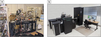
Based on these ideas, in 1994, Larson, Camus, Holzman, and Kelly incorporated MMillennium Instruments. Kelly and Larson carried this forward, but it was not until about 1998 that the first employee was hired, Gribb, the third honoree on the MRS Innovation in Materials Characterization award. It took us about two years to build the alpha prototype, Figure 6a. Note that the alpha prototype had two ultrahigh vacuum SEMs mounted on the side for positioning the tip relative to the local electrode. At the turn of the millennium, we changed our name to Imago Scientific Instruments. In 2002, Mike Miller at Oak Ridge National Laboratory purchased our voltage-pulsed beta prototype instrument, which was delivered in 2003. We started working on laser-pulsed LEAP in earnest in 2002, and in 2006, we shipped the first commercial laser-pulsed atom probe. In 2006, Imago acquired a competitor, Oxford Nanoscience. In 2010, Imago was acquired by Ametek, and we are now part of Cameca Instruments. A photograph of today’s LEAP 4000 is shown in Figure 6b for comparison with the alpha prototype. The system has obviously come a long way from its initial incarnation.
(a) Photograph of the alpha prototype of the commercial local-electrode atom probe (LEAP) at Imago Scientific Instruments (2001). (b) Photograph of a current LEAP 4000 system for comparison with the alpha prototype.

In order for all of these developments to be realized, we needed a lot of things to happen at the right time. We were contemplating generating terabytes of data in 1998; that was a scary thought then, but nowadays, it is not a problem. The CPUs and the graphical processing units back then were not up to processing a hundred-million-atom data set, visualizing it, and so on. The only known way to cool a specimen to 20 K without vibration was using liquid helium, which was a less than desirable option. Fortunately, commercial vibration-isolated mechanical refrigeration systems appeared in 2000 just in time for our needs. The lasers were not stable enough for a commercial offering. The first suitable laser for small-spot laser pulsing became commercially available about one year prior to our adoption. Most importantly, commercial FIB tools did not exist 20 years ago. Given all of this, we now identify three crucial technologies that contributed to the second revolution in APT: (1) the local-electrode geometry, (2) FIB-based specimen preparation, and (3) thermal pulsing primarily with lasers.
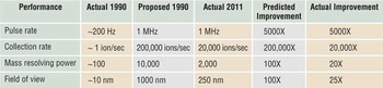
In reviewing the developments of the past 20 years, it is instructive to return to the meeting of the International Field Emission Society in Albuquerque, NM in 1990. Müller founded this society. There was a talk by Kelly and his coauthors regarding his predictions for the future of APT. There are a number of things contained in the two papersReference Kelly, Mancini, McCarthy and Zreiba27, Reference Kelly, Zreiba, Howell and Bradley28 published at that meeting, and basically he said we should pulse at a million hertz; we should collect data at hundreds of thousands of ions per second; we should have mass resolving powers in the vicinity of ten thousand; and we should have fields of view on the order of hundreds of nanometers. That was followed by a prediction at the MRS Fall Meeting in 1993 of things that we felt would be happening in the 21st century,Reference Kelly, Camus, Larson and Holzman33Table I.
Comparison of predictions (1990) with reality (2011) for performance of atom probes.

How radical were these predictions? It was 20 years ago, and at that time, pulse repetition rates were a couple of hundred Hertz. Kelly stood up and said, “I want a million hertz, and 200,000 atoms per second, and mass resolving power, and field of view improvements of two orders of magnitude.” What did the people at this conference say? The French group from the Université de Rouen at this conference decided that Kelly was the Jules Verne of APT, which is the origin of our motivation in preparing this presentation for the MRS Spring Meeting in 2011. It is relatively safe to say that many of the predictions have come true.
FIB-based specimen preparation
The second-third of the second revolution is making appropriate samples for an atom probe from a disparate array of materials. Historically, people have wanted to do site-specific sample preparation for atom probes, where the specimen is obtained from a chosen location, such as a grain boundary, rather than from a random location. Almost 30 years ago, Waugh et al.Reference Waugh, Payne, Worrall and Smith34 made the first attempts to prepare specimens for APT using directed ion beams. About 23 years ago, in what we consider to be the precursor to FIB milling for atom probe preparation, Kathy Alexander and her colleagues at Oak Ridge National Laboratory were using a Gatan “precision ion milling system,” or PIPS, to modify specimens for APT.Reference Alexander, Angelini and Miller35 These early instruments did not have the performance to do the job, but this was the precursor to the FIB work that came in the late 1990s. Larson et al.Reference Larson, Foord, Petford-Long, Liew, Blamire, Cerezo and Smith6 proposed two methods in 1998: one was where ions are scanned in an annular pattern, and then the pattern is made smaller until a sharp needle is formed. A second method involves a sort of whittling away at the sample until a needle is formed. The first method has become the standard method and is currently used by most groups. However, one still could not go into an arbitrary wafer surface or piece of material and find a region of interest and take it out. In the mid-2000s, there began a capitalization on TEM preparation techniques that were being developed in the FIB, which became known as “liftout” methods.
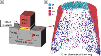
There are two early patents from ImagoReference Kelly, Martens and Goodman36 in 2001 that call for taking a piece out of an arbitrary bulk chunk and putting it in the FIB to sharpen it. Miller and colleaguesReference Miller, Russell and Thompson37, Reference Miller38 at Oak Ridge National Laboratory in 2005 showed that this was feasible, and then work by Thompson and his colleaguesReference Thompson, Lawrence, Larson, Olson, Kelly and Gorman39 in 2006 laid the basic groundwork for techniques that are being used today. We found in this work that finishing up with a low-ion-energy milling stage was critical to preparing quality samples. Next came the dual-beam FIB, which is the current state of the art, and we were able to do high-quality imaging of the specimen with electrons without damage, and then use the FIB only when needed in order to shape the samples. If this is done successfully, we can obtain data such as in Figure 7, which shows a source, drain, channel, and gate oxide in schematic, and a data set from a current generation Intel i5-650 transistor that was de-processed and analyzed in the atom probe. We recently presented this work at the Microscopy of Semiconducting Materials 2011 conference in Cambridge.Reference Larson, Lawrence, Lefebvre, Olson, Prosa, Reinhard, Ulfig, Clifton, Bunton, Lenz, Renaud, Martin, Kelly, Walther, Midgley and Cullis40 Though this type of specimen analysis is not yet routine, the work shows the promise that it will soon be realized.
Atom probe tomography analysis of a high-κ + metal gate transistor: gate oxide/source/channel/drain region. (a) Schematic of the transistor (after MardinlyReference Mardinly, Cullis and Midgley41) and (b) an atom map of the transistor.Reference Larson, Lawrence, Lefebvre, Olson, Prosa, Reinhard, Ulfig, Clifton, Bunton, Lenz, Renaud, Martin, Kelly, Walther, Midgley and Cullis40

Laser pulsing
About one decade after the invention of the atom probe, Kellogg and TsongReference Kellogg and Tsong42 began experiments with the pulsed-laser atom probe. An important part of the first atom probes was that in voltage pulsing: the specimen must have a high electrical conductivity, like that of metals. With laser pulsing, which operates by thermally pulsing the field evaporation, the electrical conductivity does not matter, so nonmetals can be analyzed. Kellogg and Tsong showed that semiconductor materials, glasses, and metals could be analyzed with laser pulsing. The technique did not catch on much, however, because in 1980, lasers were slow, expensive, and unstable. The first 30 years of atom probes was dominated by metals research for this reason. Eventually, given the compelling reasons for using laser pulsing to analyze insulating materials coupled with advances in laser technology, thermal pulsing caught on. The first commercial laser atom probes were offered in 2005 by all of the commercial vendors at the time. Now, virtually every commercial atom probe has a laser. In addition, laser pulsing produces a very low energy spread on the ions. This means it is possible to get very high mass resolving power for long flight times. Liu and TsongReference Liu, Wu and Tsong43 built an 8-meter-long pulsed-laser atom probe that achieved mass resolving powers of 4000.
A look to the future
Given this review of the history of the atom probe, it is interesting to consider where the technology may be headed. Certainly, one direction is how to achieve the ultimate atom probe. A group comprised of Mike Miller of Oak Ridge National Lab, Krishna Rajan of Iowa State University, Simon Ringer of the University of Sydney, and Kelly has proposed the ATOM ProjectReference Miller and Kelly44, Reference Kelly, Miller, Rajan, Ringer, Borisevich, Dellby and Krivanek45 to the U.S. Department of Energy to build a next-generation instrument called the atomscope. The question we hope to address is, “Can atomic-scale tomography be achieved?” That is, “Can we see every atom in a three-dimensional volume of technologically relevant size?” We want to detect 100% of the atoms and position them precisely enough that we may see defects or infer defects. With this information, crystal structure determination in real space would be enabled. If we can supplement that with chemical information such as from electron energy loss spectroscopy, structural information from diffraction patterns, and maybe some physical properties measurements such as inner potential measurements, that would be atomic-scale tomography with major enhancements. Furthermore, with knowledge of every atom, computational materials science would be able to predict physical properties and close the loop on structure-properties relationships.
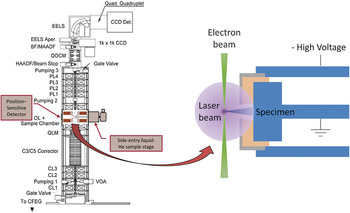
Is this science fiction? The approach we are taking curiously goes back to electron microscopes. We will use an ultrahigh-vacuum scanning transmission electron microscope (STEM) with aberration correction by Nion.Reference Krivanek, Dellby and Lupini46 If we introduce an atom probe into the electron microscope such that the specimen can be imaged and field evaporated, Figure 8, then we get the benefits of imaging from the electron beam with the analysis of the atom probe. The specimen shall be rotated fully, 360 degrees, and the atom probe part will reside inside the pole piece of the STEM. The laser would impinge from the side at any angle in the horizontal. This will allow us to image the specimen with regularity and use the specimen apex shape obtained from surface tangent tomography.Reference Petersen and Ringer47, Reference Petersen and Ringer48 If we know the specimen’s apex shape, then, in principle, we can perfect data reconstruction for every atom that is field evaporated, which is the target.
The Atomscope as proposed in the ATOM Project.Reference Miller and Kelly44, Reference Kelly, Miller, Rajan, Ringer, Borisevich, Dellby and Krivanek45 Left: A schematic diagram of the electron column with an atom probe component in the objective lens module. Right: Specimen geometry with an integrated local electrode.

But what about getting to 100 percent detection efficiency? There are detectors based on superconductorsReference Irwin49 that may do the job. Cooper-paired electrons have a very small binding energy of about 3 meV in metallic superconductors. These become very sensitive signal generators: If an incoming ion arrives with 5 keV and hit something with a 3 meV binding energy, one million broken Cooper pairs result. The freed electrons can be differentiated from the Cooper pairs, and the resulting signal is adequate for the job. In principle, we think we can configure an atom probe detector that will get 100 percent detection efficiency (or maybe 99.9%). An interesting property of these detectors is that the number of Cooper-paired electrons broken is proportional to the incoming energy, so a kinetic-energy signal is available. Current time of flight spectroscopy has some peak interferences such as 14N+ at m/n=14 overlaps with 28Si++. For the same accelerating potential, 14N+ and 28Si++ would have very different kinetic energies. So rather than discriminate these ions based solely on time of flight, we would now discriminate them based on time of flight and kinetic energy.Reference Kelly50 This makes the time of flight precision required much less challenging and allows us to relax some design constraints on the instrument geometry. For example, we may shorten the flight path length, which increases the field of view, just like Panitz’s IAP.Reference Panitz2 The future is beginning to look like the past.
There is another thing that could happen here. We could configure the instrument such that the ions field evaporate solely during periods of slightly elevated applied voltage (i.e., a voltage pulse).Reference Kelly50 If there is any evaporation event or noise that hits the detector between pulses, it would show up at a lower kinetic energy, maybe 4 keV, and the data would be generated during a momentary rise to 5 keV. This would allow us to separate the noise from the data. “Noise-free” imaging would be revolutionary for atom probes. It would also allow us to separate field ions created between pulses from atom probe data created during pulses, as illustrated in Figure 4. Furthermore, we may get enough energy resolving power to unravel the energy spread that occurs in voltage pulsing so we would not need reflectrons. Because peak discrimination would be much better, we could use a shorter flight path length that yields a larger solid angle and higher repetition rates. If we can go to a couple hundred picoseconds flight times through higher voltages, we would be able to work with blunter specimens, which gives a larger field of view and would enable 5 megahertz pulse repetition rates.
If we can deliver noise-free imaging, 100 percent detection efficiency, and putting all the atoms on the crystal lattice, atom probes will have reached another major plateau: atomic-scale tomography.Reference Kelly, Miller, Rajan, Ringer, Borisevich, Dellby and Krivanek45, Reference Kelly, Miller, Rajan and Ringer51 Democritus would be impressed.
Acknowledgments
The authors would like to note that Tye Gribb was also listed as an honoree for the Innovations in Materials Characterization Award. Anybody who has worked on a team building an instrument of this complexity understands that there is a large group of people who has contributed a lot to make this happen, and the three of us are the figureheads accepting this award for the entire team that was originally Imago Scientific Instruments and is now Cameca Instruments, Inc. The assistance of John Panitz in recounting the early history of the atom probe is gratefully acknowledged. We would also like to note that this effort would not be possible without sustained financial investment, and there are numerous private and institutional investors whose interest and shared vision have made this dream a reality. The authors would like to thank David Larbalestier for his enthusiasm and willingness to share the dream and commit resources in the early days to make this all happen. Finally, we would like to thank David Seidman, who has been a very strong and ardent supporter of our efforts, a consumer of our products, and is the person who nominated us for this award.
Thomas F. Kelly is division vice president responsible for atom probe technology and operations at Cameca Instruments, Inc. He received his PhD degree (1981) in materials science from the Massachusetts Institute of Technology. Among his awards are the Presidential Science Award from the Microbeam Analysis Society (2008) and part of the Image team receiving three R&D 100 Awards (2004, 2006, and 2008). He has 10 patents issued and pending and over 150 publications. Kelly can be reached by email at thomas.kelly@ametek.com.
David J. Larson is director of atom probe technology at Cameca Instruments, Inc. He received his PhD degree (1996) in materials science from the University of Wisconsin, Madison. His honors include the position of Visiting Scholar in Corpus Christi College at the University of Oxford, honorary staff in the Key Centre for Microscopy and Microanalysis at the University of Sydney, and the Burton Medal for distinguished contributions to the field of microscopy and microanalysis from the Microscopy Society of America. Larson has 10 patents granted or pending and over 180 publications. Larson can be reached by email at david.larson@ametek.com.