I. INTRODUCTION
Photocatalytic and photoelectrochemical fuel generation provide an appealing route to meet the demand of renewable energy supply. Since discovery of solar water splitting with TiO2 in 1970s, Reference Fujishima and Honda1 semiconductor-based photocatalysis has been intensively investigated. However, no single semiconductor can meet the need of photocatalytic and photoelectrochemical water splitting so far. Reference Li and Wu2 For example, TiO2 shows poor visible-light absorption due to its large band gap (E g = 3.2 eV). Reference Li and Wu2,Reference Walter, Warren, McKone, Boettcher, Mi, Santori and Lewis3 Although narrow band gap semiconductors, such as Fe2O3 (E g = 2.1 eV) and BiVO4 (E g = 2.4 eV), allow for visible-light absorption, they suffer from severe charge recombination. Reference Li and Wu2,Reference Kim and Choi4 Formation of composites is an alternative route to mitigate the concerns of single semiconductors. For instance, deposition of gold nanoparticles on the semiconductor surface has been extensively used to improve the performance of semiconductors in photocatalysis and photoelectrochemical fuel generation. Reference Cushing and Wu5–Reference Atwater and Polman8 However, the underlying mechanism of performance improvement is still under debate because gold nanoparticles may play different roles in different cases.
Gold nanoparticles exhibit strong localized surface plasmon resonance (LSPR) under solar radiation. Reference Cushing and Wu5 If gold nanoparticles are coupled to a semiconductor in an effective way, the plasmonic energy stored in the gold nanoparticle can transfer to the semiconductor, inducing charge separation in the semiconductor. Reference Cushing and Wu5,Reference Cushing, Li, Meng, Senty, Suri, Zhi, Li, Bristow and Wu9–Reference Li, Cushing, Zheng, Meng, Chu and Wu14 Hence gold nanoparticles have been deposited on the semiconductor surface to utilize plasmon to enhance solar energy conversion. Besides the plasmonic effect, gold nanoparticles on the semiconductor surface may play other roles. The Schottky junction can be formed at the gold–semiconductor interface when the metal and the semiconductor are brought together. The intimate contact between each other causes a shift of the Fermi level to reach an equilibration at the interface. As a result, the photo-generated electrons can transfer from the semiconductor to the gold nanoparticles. Reference Subramanian, Wolf and Kamat15,Reference Choi, Chen and Kamat16 Hence the charge extraction can be enhanced by the Fermi level equilibration. Furthermore, the gold nanoparticles on the semiconductor surface may serve as co-catalyst that promotes the redox reaction at the semiconductor–electrolyte interface.
In the present study, hematite is used as the photoanode in a photoelectrochemical cell (PEC) to perform solar water splitting. Gold nanoparticles are deposited on the hematite surface to enhance solar energy conversion. The underlying enhancement mechanisms by the gold nanoparticles are investigated. Given that the gold nanoparticles play multiple roles, including plasmonic enhancement, Fermi level equilibration, and surface catalysis, we attempt to distinguish these roles and to examine which role is dominant in enhancement of solar energy conversion. For comparative study, the gold@silica core–shell nanoparticles are also immobilized on the hematite photoanode surface. The presence of silica shell can prevent the effect of Fermi level equilibration.
II. EXPERIMENTAL
A. Synthesis of hematite nanorod array
The hematite (α-Fe2O3) nanorod array was synthesized according to a well-developed hydrothermal method. Reference Li, Cushing, Zheng, Meng, Chu and Wu14,Reference Vayssieres, Beermann, Lindquist and Hagfeldt17 A precleaned fluorine-doped tin oxide substrate was placed in an autoclave with a teflon liner; and the conductive side was faced downside. The precursor solution contained 0.15 M FeCl3 and 1.0 M NaNO3; and the pH value of the solution was adjusted to around 1.5 with HCl. The autoclave was heated at 100 °C for 3 h. The obtained yellow iron hydroxide film was annealed at 550 °C for 2 h and then held at 800 °C for 20 min.
B. Deposition of Au nanoparticles on hematite nanorod
The Au nanoparticles were deposited on hematite with a co-precipitation technique. Reference Li, Cushing, Zheng, Senty, Meng, Bristow, Manivannan and Wu18 0.1 g of urea was dissolved in a 10 mL of 10 mM HAuCl4 aqueous solution and then quickly heated to 80 °C. The hematite nanorod array was immersed into this solution for 15 min. Thereafter, the hematite nanorod was thoroughly washed with deionized (DI) water, and then annealed at 450 °C for 2 h.
C. Deposition of Au@SiO2 nanoparticles on hematite nanorod
Au nanoparticles were first prepared with sodium citrate reduction method. Reference Cushing, Li, Meng, Senty, Suri, Zhi, Li, Bristow and Wu9 Then a 5 nm thick SiO2 layer was coated on the Au nanoparticles by hydrolysis of the sodium silicate solution. Reference Cushing, Li, Meng, Senty, Suri, Zhi, Li, Bristow and Wu9 The resulting Au@SiO2 nanoparticles were then functionalized with 2-[methoxy(polyethyleneoxy)propyl]trimethoxysilane monolayer, which can be hydrolyzed in water to yield the –COOH group. The hematite nanorod was then immersed into the aqueous solution containing the Au@SiO2–COOH nanoparticles for 24 h (Fig. S1). Finally, the Au@SiO2–hematite was washed with DI water and annealed at 350 °C for 1 h. Herein, the silane monolayer was used as the organic linker to ensure the Au@SiO2 nanoparticles immobilized on the hematite surface. After heat treatment at 350 °C, the organic linker disappeared but the Au@SiO2 nanoparticles remained on the hematite surface.
D. Characterization
Field-emission scanning electron microscope (FE-SEM, JEOL 7600F, JEOL Ltd., Peabody, Massachusetts) and a transmission electron microscope (TEM; JEM 2100F, JEOL Ltd.) were used to observe the morphology and structure of the hematite nanorod and the Au nanoparticles. A Shimadzu 2550 UV-VIS spectrometer (Shimadzu Corp., Tokyo, Japan) was used to acquire the UV-Visible light absorption spectra for the slid-state film and the aqueous solution samples. X-ray photoelectron spectroscopy (XPS; PHI 5000 Versa Probe system, Physical Electronics, Chanhassen, Minnesota) was used to determine the chemical status of elements.
E. Photoelectrochemical performance measurement
Photoelectrochemical testing was carried out in a 1.0 M NaOH solution with a three-electrode PEC using a Gamry Reference 3000™ Potentiostat (Gamry Instruments, Warminster, Pennsylvania). Hematite worked as the working electrode, the Pt wire as the counter electrode and the Ag|AgCl as the reference electrode. A 300 W of Xe lamp with an AM 1.5 G filter was used as the light source. Band- and long-pass filters were used to adjust the wave length region of incident light. Mott–Schottky (M–S) plots were obtained at an AC frequency of 10 kHz using an AC amplitude of 10 mV with a three-electrode configuration. The wave length-dependent incident photo-to-electron conversion efficiency (IPCE) plots were acquired at a bias of 1.23 V versus a reversible hydrogen electrode (RHE) according to the following equation, Reference Li, Cushing, Zheng, Meng, Chu and Wu14
 $${\rm{IPCE}} = {{1240 \times J} \over {\lambda \times {{ I}_{{\rm{light}}}}}}\quad ,$$
where J and I light are the photocurrent and the light intensity measured at the wave length of λ, respectively.
III. RESULTS
A. Microstructure
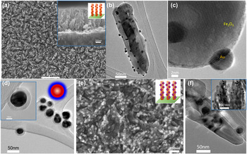
Figure 1(a) shows that the hematite nanorod array had a diameter of 40–50 nm with a height of around 850 nm. Around 10 nm sized Au nanoparticles were dispersed on the surface of hematite nanorods [Fig. 1(b)]. The measured lattice fringes in the high resolution TEM (HRTEM) images corresponded to Au and hematite [Fig. 1(c)]. XPS analysis confirmed the presence of the metallic Au and the oxidized iron in the sample (Fig. S2). For the Au@SiO2 nanoparticles, the average size of Au core was 25 nm and the SiO2 shell thickness was ∼6.5 nm [Fig. 1(d)]. The top-view scanning electron microscope (SEM) image of Au@SiO2/hematite revealed that the Au@SiO2 particles were dispersed on the hematite nanorod array [Fig. 1(e)], which was further confirmed by the TEM observation [Fig. 1(f)].
Au and Au@SiO2 nanoparticles on the hematite nanorod. (a) SEM, (b) TEM, and (c) HRTEM images of the Au/hematite. The inset in (a) shows the cross-section view of the nanorod array. (d) TEM image of Au@SiO2 with the inset showing the magnified view. (e) SEM and (f) TEM images of the Au@SiO2/hematite nanorod array.

B. Optical enhancement
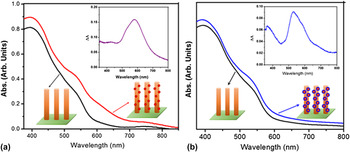
The introduction of Au nanoparticles on the hematite nanorod surface can improve the light absorption due to the plasmonic effect. Figure 2 shows the ultraviolet–visible absorption spectra for the hematite nanorod array before and after deposition of the plasmonic nanoparticles. The bare hematite nanorod array exhibited a light absorption edge up to ∼600 nm, corresponding to a band gap ∼2.1 eV. The light absorption enhancement was calculated by subtracting the absorption curve of metal/hematite with that of hematite, as shown in the insets in Fig. 2. The light absorption enhancement matched the LSPR bands of Au and Au@SiO2 particles, respectively (Fig. S3). Compared to the bare Au nanoparticles in aqueous solution, a red shift of LSPR peak was observed due to the relatively large refractive index of hematite. The insulating SiO2 layer made the LSPR peak change little compared to the free-standing Au@SiO2 in aqueous solution.
UV-Visible spectra of hematite, Au/hematite (a) and Au@SiO2/hematite (b) nanorod arrays. The insets show the light absorption enhancement due to the plasmonic effect. Note that the absorption spectra were obtained by measuring the same hematite nanorod array before and after deposition of Au or Au@SiO2 plasmonic nanoparticles.

C. Photoelectrochemical performance
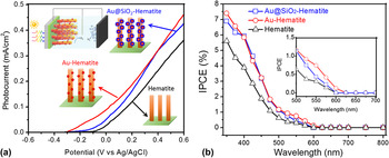
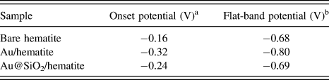
The hematite nanorod array was used as the photoanode in a three-electrode PEC for solar water splitting [see the inset in Fig. 3(a)]. The photocurrent–voltage (J–V) curves show that the photocurrent was enhanced after deposition of both Au and Au@SiO2 nanoparticles. The photocurrents at 1.23 V versus RHE (0.23 V versus Ag|AgCl) of Au/hematite and Au@SiO2/hematite were close to each other, but the onset potential shifted negatively −0.16 V after deposition of Au nanoparticles on hematite. Deposition of Au@SiO2 nanoparticles led to a smaller negative shift (0.08 V) of the onset potential [Fig. 3(a)].
J–V curves (a) and IPCE curves (b) for hematite, Au/hematite and Au@SiO2/hematite. The inset in (a) illustrating the three-electrode PEC for water splitting. The inset in (b) shows the wave length range between 500 and 700 nm.

The wave length-dependent IPCE spectra were acquired under irradiation of monochromatic light at a bias of 1.23 V versus RHE as shown in Fig. 3(b). Above 650 nm, all samples showed a negligible photocurrent, but an increase between 500 and 600 nm can be seen in Au/hematite due to the plasmonic effect.
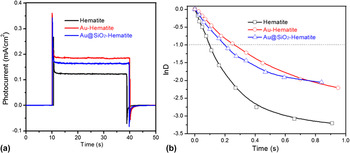
Transient photocurrent was measured to investigate the charge recombination behavior of the photoanodes (Fig. 4). A parameter (D) was introduced as
 $$D = {{\left( {{I_{\rm{t}}} - {{I}_{{\rm{st}}}}} \right)} \mathord{\left/ {\vphantom {{\left( {{I_{\rm{t}}} - {{\rm I}_{{\rm{st}}}}} \right)} {\left( {{I_{{\rm{in}}}} - {{\rm I}_{{\rm{st}}}}} \right)}}} \right. \kern-\nulldelimiterspace} {\left( {{I_{{\rm{in}}}} - {{I}_{{\rm{st}}}}} \right)}}\quad ,$$
where I t, I st, and I in are the time-dependent, steady-state, and initial photocurrent, respectively. Reference Li, Cushing, Zheng, Meng, Chu and Wu14,Reference Tafalla, Salvador and Benito19 The transient time constant is defined as the time when ln D = −1 in the normalized plots of ln D–t, which reflects the behavior of charge recombination. After deposition of Au nanoparticles on hematite, the transient time constant increased from 0.09 s to 0.27 s, which indicated the suppression of charge recombination. After deposition of Au@SiO2 nanoparticles on hematite, the transient time constant became 0.19 s.
Transient photocurrents (a) and dynamic time/ln D–t plots (b) for hematite, Au/hematite and Au@SiO2/hematite, respectively.

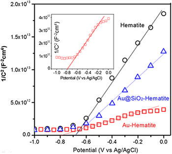
A M–S plot was used to understand the charging effect induced by the Au and Au@SiO2 nanoparticles on the hematite surface. The M–S plots were acquired at an AC frequency of 10 kHz with an AC amplitude of 10 mV (Fig. 5). The intercept represents the flat-band potential (Table I), and the slope reflects the charge carrier density in the electrode. Reference Khan, Chuan, Yousuf, Chowdhury and Cheng20 As shown in Fig. 5 and Table I, deposition of Au nanoparticles on hematite led to a negative shift of the flat-band potential from −0.68 V to −0.8 V and made the slope smaller, indicating higher charge carrier density in the electrode. In contrast, deposition of Au@SiO2 nanoparticles on hematite did not change the flat-band potential although it increased the carrier density in the electrode.
M–S plots for bare hematite, Au/hematite, and Au@SiO2/hematite measured under 10 mV and 10 kHz of frequency. The inset showing the enlarged plot for Au/hematite.

Onset potentials and flat-band potentials (versus Ag|AgCl).

a The onset potential read from the J–V curves.
b The flat-band potential from the M–S plots.
IV. DISCUSSION
The photocurrent of PEC depends on the following process: (i) generation of charge carriers in the photoanode by light absorption, (ii) charge migration to the photoanode surface, and (iii) charge injection into the electrolyte involving the water oxidation reaction at the photoanode/electrolyte interface. The overall photocurrent (J) is determined by
 $$J \sim \alpha \left( {h\nu } \right)\cdot{\eta _{{\rm{lifetime}}}}\cdot{P_{{\rm{inject}}}}\quad ,$$
where α(hν) is the number of photogenerated holes that heavily depends on the wave length of incident light, ηlifetime is the efficiency of hole extraction that reflects the fraction of photogenerated holes extracted to the photoanode surface, and P inject is the charge injection efficiency that reflects the fraction of photogenerated holes involved into water oxidation.
As mentioned in Sec. I, the gold nanoparticles on the photoanode surface can lead to surface catalysis, Fermi level equilibration, and plasmonic effects. If any of these effects alters any among α(hν), ηlifetime and P inject, it will change the photocurrent. When the Au nanoparticles are in direct contact with hematite, the Fermi levels will shift and a Schottky barrier will form [Fig. S4(b)]. Reference Li and Wu2,Reference Khan, Chuan, Yousuf, Chowdhury and Cheng20 The flat-band potential represents the potential offset at the semiconductor/electrolyte interface. The negative shift of the flat band potential upon illumination increases the band bending while not changing the Fermi level equilibration. When hematite is excited, the photogenerated electrons in the semiconductor can transfer to the neighboring Au nanoparticles, leading to accumulation of electrons in the Au nanoparticles [Fig. S4(b)]. This is reflected as a negative shift of the flat band potential (Fig. 5), Reference Subramanian, Wolf and Kamat15,Reference Choi, Chen and Kamat16,Reference Meng, Cushing, Li, Hao and Wu21 The Fermi level equilibration and the resulting charge separation between metal and semiconductor extended the lifetime of charge carriers, as evidenced in the transient time constant of Au–hematite being three times that of bare hematite (Fig. 4). The gold nanoparticles also resulted in a negative shift of the onset potential in the J–V curve [Fig. 3(a)]. Such surface catalysis effect reduced the overpotential of PEC water oxidation on the hematite photoelectrode. Reference Meng, Cushing, Li, Hao and Wu21–Reference Formal, Teetreault, Cornuz, Moehl, Graetzel and Sivula24
An IPCE enhancement can be defined by dividing the IPCEAu/hematite by IPCEhematite, which by Eqs. (1) and (3) gives
 $${\rm{IPC}}{{\rm{E}}_{{\rm{enchancement}}}} = {{\left[ {\alpha {{\left( {h\nu } \right)}_{{{{\rm{Au}}} \mathord{\left/ {\vphantom {{{\rm{Au}}} {{\rm{hematite}}}}} \right. \kern-\nulldelimiterspace} {{\rm{hematite}}}}}}\cdot{\eta _{{{{\rm{lifetime,}}\,{\rm{Au}}} \mathord{\left/ {\vphantom {{{\rm{lifetime,}}\,{\rm{Au}}} {{\rm{hematite}}}}} \right. \kern-\nulldelimiterspace} {{\rm{hematite}}}}}}\cdot{P_{{{{\rm{inject,}}\,{\rm{Au}}} \mathord{\left/ {\vphantom {{{\rm{inject,}}\,{\rm{Au}}} {{\rm{hematite}}}}} \right. \kern-\nulldelimiterspace} {{\rm{hematite}}}}}}} \right]} \mathord{\left/ {\vphantom {{\left[ {\alpha {{\left( {h\nu } \right)}_{{{{\rm{Au}}} \mathord{\left/ {\vphantom {{{\rm{Au}}} {{\rm{hematite}}}}} \right. \kern-\nulldelimiterspace} {{\rm{hematite}}}}}}\cdot{\eta _{{{{\rm{lifetime,}}\,{\rm{Au}}} \mathord{\left/ {\vphantom {{{\rm{lifetime,}}\,{\rm{Au}}} {{\rm{hematite}}}}} \right. \kern-\nulldelimiterspace} {{\rm{hematite}}}}}}\cdot{P_{{{{\rm{inject,}}\,{\rm{Au}}} \mathord{\left/ {\vphantom {{{\rm{inject,}}\,{\rm{Au}}} {{\rm{hematite}}}}} \right. \kern-\nulldelimiterspace} {{\rm{hematite}}}}}}} \right]} {\left[ {\alpha {{\left( {h\nu } \right)}_{{\rm{hemitate}}}}\cdot{\eta _{{\rm{lifetime,}}\,{\rm{hemitate}}}}{\rm{\cdot}}{P_{{\rm{inject,}}\,{\rm{hemitate}}}}} \right]}}} \right. \kern-\nulldelimiterspace} {\left[ {\alpha {{\left( {h\nu } \right)}_{{\rm{hemitate}}}}\cdot{\eta _{{\rm{lifetime,}}\,{\rm{hemitate}}}}{\rm{\cdot}}{P_{{\rm{inject,}}\,{\rm{hemitate}}}}} \right]}}\quad .$$
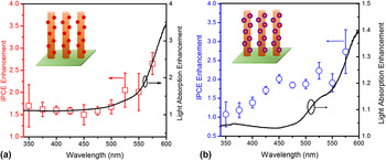
Neither the Fermi level equilibration nor the surface catalysis effects have an influence on α(hν), the number of carriers excited per incident absorbed photon. Instead, the Fermi level equilibration alters ηlifetime and P inject; and the surface catalysis increases P inject, both of which are independent of the wave length of incident light. This is seen in Fig. 6(a), showing a constant IPCE enhancement of ∼1.5 by the presence of Au nanoparticles below 500 nm.
IPCE enhancement for (a) Au–hematite and (b) Au@SiO2–hematite. The IPCE enhancement was calculated by IPCEAu/hematite/IPCEhematite.

In the wave length range of 500–650 nm, the LSPR was excited in the Au/hematite sample [Fig. 2(a)]. It increased the IPCE in this wave length range as shown in the inset in Fig. 3(b). The LSPR can enhance the charge separation in hematite [Fig. S4(a)]. That is, it would increase α(hν), which heavily depended on the wave length of incident light, as shown in Fig. 6(b). It is worth noting that the LSPR effect made a little contribution to the overall enhancement of photocurrent in the present work. The plasmonic enhancement in the metal–semiconductor composites depends on many parameters such as the size, morphology, loading level, geometry, and interface. Reference Thomann, Pinaud, Chen, Clemens, Jaramillo and Brongerman25–Reference Wang, Peng, Hu, Zhang, Hu, Li, Wang, Meng and Lee28 High-efficiency plasmonic metal–semiconductor photocatalysts or photoelectrodes must be designed to enable strong interaction between the plasmonic metal and the semiconductor. Reference Cushing and Wu5 When a plasmonic metal nanostructure is coupled strongly to a semiconductor, the plasmon can enhance the solar energy conversion dramatically. Reference Cushing, Li, Meng, Senty, Suri, Zhi, Li, Bristow and Wu9,Reference Li, Cushing, Zheng, Meng, Chu and Wu14 However, deposition of random small plasmonic metal nanoparticles on the semiconductor surface or simple mixing of small plasmonic metal nanoparticles with semiconductor particles generally leads to very weak interaction between the plasmonic metal and the semiconductor. As a result, the contribution of plasmon to overall solar energy conversion is very limited although the plasmonic metal nanoparticles show strong absorption of sunlight.
In this work, an alternative treatment of hematite surface was the conjugation of hematite with the Au@SiO2 core–shell nanoparticles via a silane monolayer and the follow up heat treatment. Such surface-modification process led to passivation of hematite surface. This reduced the surface states [Fig. S4(c)] that acted as the surface traps of charge carriers (or called as the charge recombination sites), Reference Formal, Teetreault, Cornuz, Moehl, Graetzel and Sivula24,Reference Sivula29–Reference Formal, Graetzel and Sivula31 which was confirmed by the facts that deposition of Au@SiO2 nanoparticles on hematite prolonged the lifetime of charge carriers [Fig. 4(b)]; and there was not any hump in the ICPCE curve of Au@SiO2/hematite as shown in the inset in Fig. 3(b). Surface passivation altered α(hν), ηlifetime, and P inject. Consequently, the IPCE enhancement in Fig. 6(b) was not constant with change in the wave length of incident light.
It is well known that plasmon can enhance the solar energy conversion of a neighboring semiconductor via three mechanisms Reference Cushing and Wu5 : light scattering/trapping, plasmon-induced resonance energy transfer (PIRET) Reference Cushing, Li, Meng, Senty, Suri, Zhi, Li, Bristow and Wu9 and direct electron transfer Reference Tian and Tatsuma11 (DET, also called hot electron injection). Light scattering is evident only when the nanoparticles are large (typically >50 nm). For Au@SiO2/hematite, the plasmon made a negligible contribution to overall solar energy conversion, as indicated in Figs. 6(b) and 3(b). This is not surprising if we keep in mind that the near-field plasmon-enhancement was almost impossible due to: (i) the integral of spectral overlap between the LSPR of particles with the absorption band of hematite was very small, which was unfavorable to the PIRET process; (ii) the SiO2 shell blocked the DET from gold to hematite. The presence of silica shell also excluded the Fermi level equilibration effect in Au@SiO2/hematite.
V. CONCLUSIONS
When bare gold nanoparticles were deposited on the hematite photoanode surface, the photoelectrochemical current enhancement of PEC was originated from combination of the Fermi level equilibration, surface catalysis, and LSPR effect of gold nanoparticles. The Fermi level equilibration and the surface catalysis effects were dominant while the plasmonic effect made a little contribution to the photoelectrochemical current enhancement. The surface catalysis effect reduced the overpotential of water oxidation reaction, and the Fermi level equilibration effect reduced the charge recombination rate. In contrast, in the Au@SiO2/hematite samples, the LSPR of Au@SiO2 nanoparticles had a negligible effect on the photoelectrochemical current although LSPR led to light absorption. The Fermi level equilibration and surface catalysis effects were excluded in the Au@SiO2/hematite samples while the photoelectrochemical current enhancement in the Au@SiO2/hematite samples was mainly due to surface passivation. The results show that the enhancement of photocurrent from plasmonic metal nanoparticles cannot be assigned to a specific enhancement without performing wave length- and time-dependent measurement. This work shows that design of effective metal–semiconductor structures is important to overcoming the charge recombination or absorption problems of a semiconductor for solar water splitting.
Supplementary Material
To view supplementary material for this article, please visit http://dx.doi.org/10.1557/jmr.2016.102.
ACKNOWLEDGMENTS
This work was financially supported by the US Army Research Laboratory (W911NF-14-2-0116) and National Science Foundation (CBET-1233795). S.K.C. and J.B. were grateful to the NSF Graduate Research Fellowship Grants (1102689). The use of WVU shared facility is acknowledged.