I. INTRODUCTION
Functional oxide membranes are of interest in energy, and environmental technologies, as well as in microelectromechanical systems and sensor devices. The ability to preserve the mechanical stability of such freestanding structures under operating conditions is important. Applications of such ultrathin membranes also exist for controlled rupturing upon reaching threshold stimuli: one can envision applications such as drug delivery across an otherwise impermeable membrane that would crack at a certain temperature, thermal/electrical fuse, and so on. For instance, mechanical rupture of several organic/inorganic membranes and capsules are finding potential applications in targeted material delivery, triggered either magnetically or thermally.Reference Hoare, Timko, Santamaria, Goya, Irusta, Lau, Stefanescu, Lin, Langer and Kohane1–Reference Liu, Liu, Liu, Chen and Chen3 Studies of functional oxide materials in such membrane structures are hence of interest.
Transitions accompanied by volume changes and consequently sharp stress changes leading to mechanical failure are an interesting approach to fabricate such structures that will abruptly break upon a critical threshold excitation. Large stress change across the phase transition has been reported for VO2 as the unit cell volume undergoes ∼0.32% shrinkage across the monoclinic–tetragonal transition at ∼67 °C. While the issues concerning the mechanical instability across the structural phase transitions in ferroelectric ceramicsReference Pohanka, Freiman and Bender4–Reference Suchicital and Payne6 and shape memory alloysReference Loughran, Shield and Leo7, Reference Xiong, Liu and Pagounis8 have been investigated, studies on VO2 in this direction are limited. Early studies on VO2 single crystals revealed microcracks and transition patterns in the form of striated structures on the surface of millimeter-sized crystals across the transition.Reference Mitsuishi9 Similarly, line cracks on the surface of epitaxial films were observed as a result of thermal stress relaxation across phase transition above a critical film thickness of 15 nm.Reference Nagashima, Yanagida, Tanaka and Kawai10 The observed microcracks also influence the electrical transport properties and introduced multiple steps in the metal–insulator transition of VO2. Polarized light microscope and x-ray reflection studies revealed reversible domain patterns across the structural phase transition leading to an interpretation of twinning.Reference Fillingham11 In general, structural transition is associated with twin formation, when symmetry of the final phase is reduced compared to the initial one. Such a transition-induced twinning was also observed in monoclinic phase of Cr-doped VO2.Reference Marezio, Dernier and Santoro12 While previous studies on microcracking and transformation twinning across the metal–insulator transition were carried out on VO2 single crystals and thin films, studies on self-supported structures are yet in their infancy. Thermally induced structural phase transition in VO2 is accompanied by an insulator–metal transitionReference Morin13 with consequently large changes in electrical and optical properties and also can be triggered by electricalReference Ruzmetov, Gopalakrishnan, Deng, Narayanamurti and Ramanathan14 and/or opticalReference Michael, Buckman, Rodger, Thierry, Patrick and Alain15 fields in the vicinity of room temperature. Hence, VO2 in the form of membranes has potential technological interest and further serves as a model system for exploration of phase transition-induced mechanical instability. Here, we report on rupture of VO2 on membranes across the thermally triggered phase transition and probe the macro- and microstructural changes by in situ optical and transmission electron microscopy (TEM).
II. EXPERIMENTAL METHODS
VO2/Si3N4 membrane structures were fabricated by depositing VO2 thin film on commercially available Si3N4 membrane (50 nm thick) windows on silicon. The thickness of the VO2 layer is ∼170 nm and lateral dimension of the membrane is 100 × 100 μm. The VO2 films on Si3N4 membrane grids were deposited by RF sputtering at 550 °C. The radio frequency (RF) source gun power was set to be 150 W. During the deposition, total pressure of 10 mTorr was maintained with the flow of operation gas mixture containing 99.75 SCCM Ar and 0.5 SCCM O2. VO2 thin films were also deposited under identical condition on 4-inch Si wafer with HfO2 buffer layer for stress relaxation measurements. Amorphous HfO2 layer of 20 nm is deposited at 250 °C on Si wafer using a Cambridge Nanotech Savannah S200 atomic layer deposition system (Cambridge, MA) prior to VO2 deposition. TEM studies were carried out using JEOL 2010F transmission electron microscope (JEOL USA, Inc., Peabody, MA) operated at 200 kV. Gatan heating holder (Gatan, Inc., Warrendale, PA) was used for in situ TEM studies from room temperature to 125 °C. Thin film stress measurements were carried out using TENCOR FLX-2320 instrument (Tencor Instruments, Milpitas, CA) by in situ wafer curvature method. Slow temperature ramping of 2 °C/min was used for the heating and cooling cycles. Resistance–temperature plots were obtained from current–voltage measurements using probe station interfaced with optical microscope for in situ imaging during the measurement.
III. RESULTS AND DISCUSSION
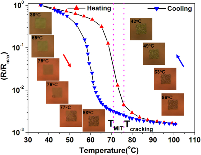
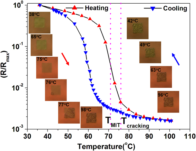
Figure 1 shows the normalized electrical resistance–temperature plot across the insulator–metal transition. The resistance measurements were carried out from room temperature to 120 °C at intervals of 5 °C/min, while the changes in the membrane stability were imaged by optical microscope simultaneously. Nearly, three orders of magnitude change in electrical resistance are observed across the insulator–metal transition that is typical for good quality VO2 films on silicon substrates. Optical microscopy images recorded across the transition show a reversible color change upon the insulator–metal transition. In addition, extensive microcracking is seen across the phase transition. The crack nucleation and propagation across the transition were captured as a movie, and the corresponding images recorded at different temperatures are shown as inset in Fig. 1. While the insulator–metal transition temperature is ∼71 °C (obtained from the derivative of resistance–temperature plot), the phase transition-induced cracks are visually observed starting at ∼76 °C. This offset is due to the fact that for electrical resistance to change significantly, it is enough for a percolating path to be created, while for global stress change and cracking, it may require a greater fraction of the sample to be transformed into the tetragonal phase. In the present case, cracks are observed around 76 °C with the optical microscope and propagate rapidly within next 2 °C of increment as the phase transition-induced stress reaches some critical value and then gradually increases in crack density up to 90 °C. Finally, the microcracks in the membrane are stabilized at ∼100 °C, and no considerable changes were observed during cooling indicating the irreversible nature of deformation.
Normalized resistance ratio of self-supported VO2/Si3N4 membrane measured in-plane as a function of temperature, while the images were captured by optical microscopy in situ. These images are shown as inset for various temperatures spanning the transition boundary.
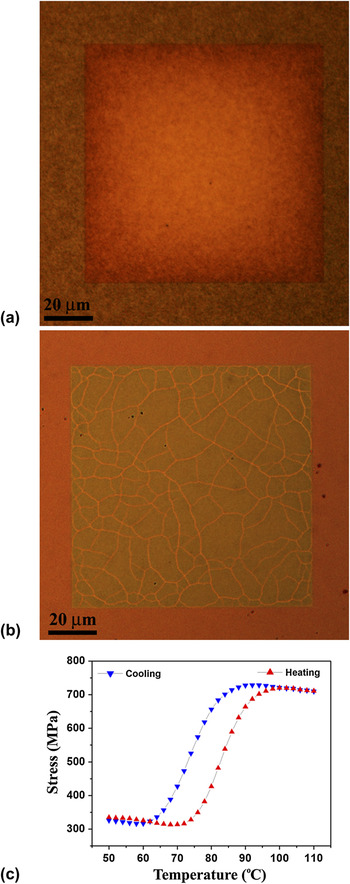
Issues concerning membrane cracking across the phase transformation can be realized from images recorded before and after thermal cycles. Figure 2(a) and 2(b) show as-prepared membrane and after subjecting to two thermal cycles. It is evident that the cracks are distributed all over the membrane. It is important to note that the VO2/Si3N4 film on Si substrate away from the membrane region is stable. This is similar to VO2 thin films deposited on rigid substrate that show stability over numerous thermal cycles in spite of large stress change across the phase transition.Reference Viswanath, Ko and Ramanathan16 Based on the observations, it is clear that the cracking occurs across the phase transition in the membrane portion of the sample. To understand the stress associated with the phase transition and cracking, the stress change across the metal insulator transition (MIT) from the VO2 thin film deposited under identical condition on a 4-inch Si wafer with HfO2 buffer layer was carried out. Figure 2(c) shows the stress–temperature plot of VO2 film showing ∼410 MPa stress change across the transition. Large tensile stress is generated across transition from low temperature monoclinic phase to high temperature tetragonal phase. The residual stress values in the case of VO2/Si3N4 membrane could be different than that for the VO2 film on a thick Si substrate due to substrate effects, whereas it is reasonable to expect the change in stress across the structural phase transition would be similar as they were deposited under identical condition. Note that the biaxial elastic modulus of Si3N4 membrane is higher (∼298 GPa) than the biaxial modulus of Si (∼180 GPa) leading to generation of high tensile stress across the transition.Reference Martins, Malhaire, Brida and Barbier17 It is important to note that the average thin film stress measured at room temperature itself is highly tensile in nature (∼350 MPa) in VO2 deposited on HfO2 layer. Indeed, the flat buckling-free VO2/Si3N4 membrane microstructure also suggests that the VO2/Si3N4 membrane is under tensile stress. In addition, volume shrinkage across the structural phase transition in VO2 on heating leads to further tensile stress generation and cracking of VO2 membrane. Onset of stress change takes place at ∼72 °C and varies as the transition temperature is spanned. The steady-state stress levels and their sensitivity toward temperature across the transition have been reported recently.Reference Viswanath, Ko and Ramanathan16 This suggests that the membrane cracking at 76 °C is associated with the phase transition-induced stress and cracking occurs when the temperature (stress) exceeds a critical value to detach/break unit area of the membrane.
Zoomed in micrograph of VO2/Si3N4 membrane (a) as-fabricated and (b) after subjecting to two thermal cycles. Extensive microcracking of the membrane is evident across the insulator–metal transition. (c) Stress–temperature plot obtained from wafer curvature measurement of VO2 thin films on HfO2/Si wafer.

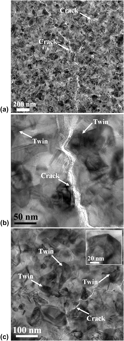
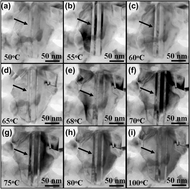
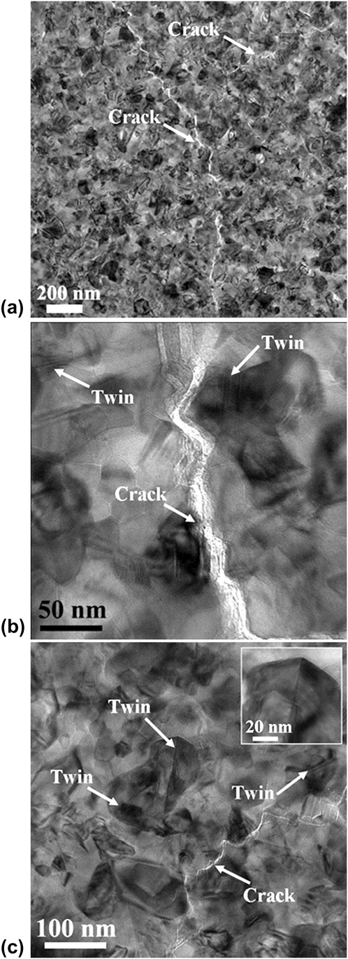
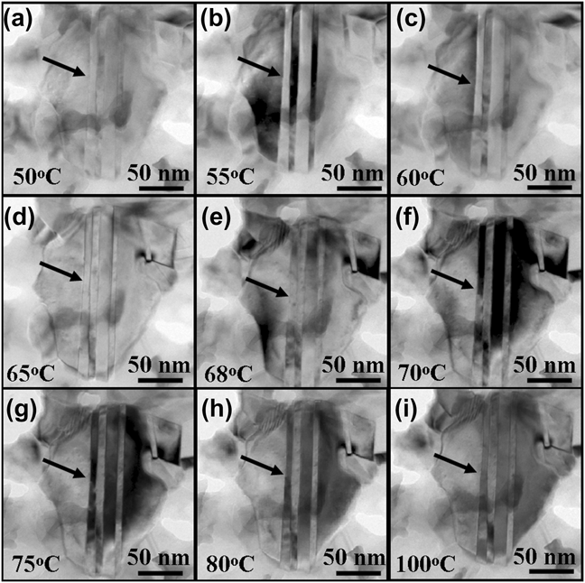
Microstructural studies have been carried out on the VO2/Si3N4 membrane to get more insights into the phase transition-induced rupture. Figure 3(a) and 3(b) shows TEM bright field images of VO2/Si3N4 membrane after thermal cycles and indicates microcracks. It is important to note that the individual VO2 crystallites appear stable away from the cracks. It has been reported that millimeter-sized single crystals of VO2 undergo extensive cracking,Reference Mitsuishi9 while polycrystalline thin films or nanostructures of VO2 show superior stability in their phase transition characteristics.Reference Fan, Huang, Cao, Ertekin, Barrett, Khanal, Grossman and Wu18, Reference Ko and Ramanathan19 This strong size effect on the mechanical stability of VO2 can be related to factors such as anisotropy in the unit cell distortion versus the orientation of the crystallites. In addition, the phase transition-induced stress scales with the size of the crystallite and hence the bulk single crystals may suffer from cracking, while the nanocrystalline or polycrystalline VO2 can relax the phase transition-induced stress. Moreover, fracture costs energy as new surfaces are formed, and it is known that fracture strength depends on surface energy and crystal size.Reference Rice and Pohanka20–Reference Rice, Freiman and Mecholsky22 Hence, bulk crystals/thick epitaxial films are prone to relax the stress by developing cracks as the elastic strain energy can balance surface energy at larger volume to surface ratio.Reference Nagashima, Yanagida, Tanaka and Kawai10 Interestingly, TEM investigations revealed twined microstructure around the cracks indicating possible plastic deformation by twinning across the phase transition. In Fig. 3(b) and 3(c), twinned crystallites are marked near the microcracks. A twinned grain at high magnification is shown as inset in Fig. 3(c). In addition, cracks are passing through the VO2 grains indicating the transgranular fracture, which is evident from the high magnification image shown in Fig. 3(b). Stress distribution and the deformation zone near crack tips have been investigated in detail by numerical simulations in literature, and the results suggest variation in the stress levels required for the twin formation near the crack regions based on microstructural factors such as orientation and grain size.Reference Fischer, Oberaigner and Waitz23–Reference Christian and Mahajan26 In situ TEM studies have been carried out to understand the origin of the twinning in VO2 membrane since both deformation twinning and phase transition-induced twinning (martensitic type) are likely. Figure 4 shows a series of TEM bright field images of twin platelets recorded at different temperatures across the phase transition. It is evident from the in situ TEM observations that the twinned platelets do not change across the phase transition except for the imaging contrast. The changes in the contrast seen across the phase transition are due to the fact that the sample is moving/bending across the phase transition leading to a slight difference in the diffraction contrast. Stable twin microstructure across the phase transition was noted in many different regions. This strongly suggests that the twinning is not necessarily associated with the phase transition. Moreover, twinning is introduced during reheating toward high symmetry tetragonal phase, which is evident from the in situ TEM observations shown in Fig. 5. The arrow in the bright field image shows twin free microstructure at 50 °C and eventually form twin platelets at around 65 °C. Further temperature change does not affect the twin microstructure. We hypothesize that the twins formed may not be directly related to phase transition rather associated with the structural transition-induced cracks that are already present. While the initial crack nucleation takes place at higher temperature than the T MIT during first thermal cycle, crack growth during subsequent cycles lead to twinning at relatively low temperatures. The crack-induced twinning is stable once it is formed, as there is no driving force for detwinning unlike the phase transition-induced twinning. It is found that the critical stress required to initiate twinning in inorganic materials can be as low as 10 MPa (calcite), 150 MPa (jadeite), and varies between 20 and 160 Mpa in many hard material systems.Reference Orzol, Trepmann, Stockhert and Shi27–Reference Tullis29 Hence, the extensive microcracking may promote twinning in VO2 membrane across the phase transition.
TEM bright field images of VO2/Si3N4 membrane recorded at different magnifications. (a) and (b) are low and high magnification bright field images showing the transgranular nature of fracture. Evidence for twinning is observed near the crack regions and marked by arrows in (b) and (c). A twinned grain recorded at high magnification is shown as inset in (c).
Stability of twin platelets observed by TEM during in situ heating (a–i) from 50 to 100 °C in the interval of 5 °C across the insulator–metal transition.
TEM bright field images show the formation of twins during in situ heating (a–i) from 50 to 100 °C across the insulator–metal transition.

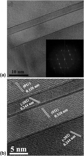
Figure 6 shows a lattice image recorded from VO2 twin platelets of ∼10 nm width and ∼200 nm length. The presence of twinning is also evidenced from the streaking of reflections in the corresponding Fast Fourier Transform shown as inset in Fig. 6(a). High resolution transmission electron microscope (HRTEM) image of the twin platelets show alternative stacking of variants corresponding to (011) and (−202) planes of monoclinic VO2 phase [Fig. 6(b)]. The composition in the vicinity of twinned regions was obtained from energy dispersive spectroscopy (EDS) spectra in the electron microscope acquired using the smallest probe size of ∼5 nm and rough estimate of O/V ratio suggests that the VO2 is nearly stoichiometric and consistent with previous studies by x-ray photoelectron spectroscopy.Reference Yang, Ko and Ramanathan30 This seems to indicate that the twinning observed in the present case is not necessarily due to vacancy coalescence (e.g., recently twin formation due to large nonstoichiometry in VOx of cubic phase has been reportedReference Li, Gauntt and Dickey31). While the nonstoichiometry could induce twinning during growth, the observed twinning during the phase transition is likely related to the cracking. This is also consistent with the sharp R–T plot that shows three orders of transition, which is characteristic of high-quality VO2 film deposited on silicon.
(a) and (b) HRTEM images of twin boundary between two neighboring variants. The corresponding Fast Fourier Transform with streaking is shown as inset in (a).

The observed difference in the insulator–metal transition temperature and crack initiation temperature provides a window of 5 °C to utilize the electrical resistance change properties without irreversible failure. On the other hand, the rupture of a freestanding membrane may be exploited for one time use such as a fuse or for controlled release when the temperature reaches a critical threshold. Note that the phase transition temperature can be tuned over several tens of degrees by doping and deposition parameters and hence increases the range of operating conditions.
IV. CONCLUSIONS
Tensile stress generated across the phase transition can lead to spontaneous cracking across the structural transition in self-supported VO2 on silicon nitride membrane. From TEM, twinning was observed proximal to cracks suggesting crack-induced plastic behavior in VO2 membranes across the transition. The in situ observations correlating the insulator–metal transition characteristics, stress relaxation, and the membrane rupture/deformation could be relevant for designing oxide membrane-based devices.
ACKNOWLEDGMENTS
Financial support from National Science Foundation CCF (Grant No 09-26148) and Focus Center Research Program in the Materials Structures and Devices Focus Center is acknowledged. This work was performed in part at the Center for Nanoscale Systems (CNS), a member of the National Nanotechnology Infrastructure Network (NNIN), which is supported by the National Science Foundation. CNS is part of Harvard University.