I. INTRODUCTION
Pure Sn and Sn-based alloys deposited on electronic components (e.g., composed of Cu) are frequently used for soldering and protection. However, since nearly 60 years it is well known that Sn coatings are very prone to the formation of filamentary Sn whiskersReference Compton, Mendizza and Arnold1, Reference Galyon2 which can potentially cause short-circuit failure of the electronic equipment during operation. Hence, the history of Sn whiskers is characterized by enormous financial damage associated with breakdowns of satellites, computer centers, and military and medical devices.Reference Galyon2 Thus, there exists a great need for reliable whisker mitigation treatments. This is an issue of, in particular recent, great technological and scientific interest.
Sn whiskers are needle-like single crystalsReference Herring and Galt3 which grow spontaneously on the surface of Sn-coated Cu substrates during aging at room temperatureReference Britton4–Reference Tu7 through continuous addition of material to their base.Reference Koonce and Arnold8 Even though the growth mechanism of a Sn whiskerReference Lee and Lee5, Reference Ellis, Gibbons, Treuting, Doremus, Roberts and Turnbull9–Reference Tu, Chen and Wu18 still remains to be revealed, the “driving force” for Sn whisker growth could be related to the build-up of residual mechanical stresses in the Sn coatingReference Lee and Lee5, Reference Tu6, Reference Lindborg15, Reference Boettinger, Johnson, Bendersky, Moon, Williams and Stafford16, Reference Tu, Chen and Wu18–Reference Kato, Akahoshi, Nakamura, Terasaki, Iwasaki, Hashimoto and Nishimura25 and thus whisker growth serves as a stress relief mechanism.Reference Lee and Lee5, Reference Hasiguti13, Reference Lindborg15–Reference Kumar, Reinbold, Bower and Chason20 After Sn deposition on a Cu substrate and subsequent aging at room temperature, Cu diffuses rapidly by an interstitial mechanism into the Sn coatingReference Tu6, Reference Dyson, Anthony and Turnbull26, Reference Anthony and Turnbull27 and the formation of the intermetallic phase Cu6Sn5 takes place on the Sn side of the Sn/Cu interface, preferentially along Sn grain boundaries.Reference Lee and Lee5, Reference Tu6, Reference Chason, Jadhav, Chan, Reinbold and Kumar19, Reference Kumar, Reinbold, Bower and Chason20, Reference Tu and Thompson28, Reference Zhang, Egli, Schwager and Brown29 Continued growth of Cu6Sn5 on the Sn side occurs along the Cu6Sn5/Sn interface by a continuous supply of Cu atoms, which takes place via Cu diffusion through Cu6Sn5 grain boundaries and interstitially in Sn.Reference Tu and Thompson28 Very recently it was shown experimentally that the growth of the intermetallic phase Cu6Sn5 along Sn grain boundaries intersecting the Sn/Cu interface induces in-plane residual compressive stresses, in combination with residual stress gradients (in out-of-planeReference Sobiech, Welzel, Mittemeijer, Hügel and Seekamp22 and in-planeReference Sobiech, Wohlschlögel, Welzel, Mittemeijer, Hügel, Seekamp, Liu and Ice23 directions) in the Sn coating, which act as driving forces for the transport of Sn atoms to the whisker nucleation site and thus control whisker growth. Whisker formation would thus not occur if the intermetallic phase Cu6Sn5 would grow only in a planar morphology at the Sn/Cu interface, as such a planar growth mode would not generate compressive residual stresses (and thus stress gradients) in the Sn coating.Reference Zhang and Schwager30, Reference Sobiech, Welzel, Schuster, Mittemeijer, Hugel, Seekamp and Muller31 Also theoretical studies based on finite-element simulations support a correlation between whisker formation, the morphology of the intermetallic phase Cu6Sn5, and the developing stress gradients.Reference Kato, Akahoshi, Nakamura, Terasaki, Iwasaki, Hashimoto and Nishimura25, Reference Sobiech, Wohlschlögel, Welzel, Mittemeijer, Hügel, Seekamp, Garza, Koyuncu, Liu and Ice32
Even though the morphology of intermetallic phase formation (i.e., growth along Sn grain boundaries) seems to be decisive for spontaneous Sn whiskering in the system Sn on Cu during aging at room temperature,Reference Lee and Lee5, Reference Tu6, Reference Kumar, Reinbold, Bower and Chason20 a rigorous explanation of the observed intermetallic phase formation along grain boundaries in the Sn coatings, as compared to such phase formation along the Sn/Cu interface (and, possibly, along Cu grain boundaries), lacks. This work aims to present a comprehensive understanding of intermetallic phase formation in the system (polycrystalline) Sn on (polycrystalline) Cu during aging at room temperature by interpreting experimental results in terms of interface thermodynamics and interdiffusion kinetics. As a result, a route to avoid whiskering can be proposed. These findings thereby also shed light on the whisker-mitigating effect of Pb in Sn coatings.
Although investigations of intermetallic phase formation are abundant (see above), a detailed, time-resolved evolution of intermetallic phase formation in the system pure Sn on pure Cu lacks.Reference Lee and Lee5, Reference Boettinger, Johnson, Bendersky, Moon, Williams and Stafford16, Reference Kato, Akahoshi, Nakamura, Terasaki, Iwasaki, Hashimoto and Nishimura25 For this reason, the current project incorporates such detailed experimental investigation by means of focused ion beam (FIB) and transmission electron microscopy (TEM) and x-ray diffraction during aging at room temperature for a period of about 1 year. On this basis, a thermodynamic and kinetic interpretation of the evolution of intermetallic phase formation was found to be possible.
II. EXPERIMENTAL
Polycrystalline Sn thin films with a thickness of about 3 μm were electrodeposited onto pure Cu substrates (commercial leadframe material) using an industrial electrolyte by employing a laboratory electrodeposition setup (for further details see Ref. Reference Sobiech, Welzel, Schuster, Mittemeijer, Hügel, Seekamp and Müller21). For x-ray diffraction analysis of phases (see below), Sn thin films with a thickness of about 1 μm were used to enhance the (relative) contribution to the diffraction pattern of the intermetallic phase growing at the film/substrate interface. Directly after Sn deposition, the surface of the specimens was rinsed with methanol and subsequently the specimens were dried and aged at room temperature (i.e., storage at ∼25 °C/25 – 50% relative humidity). The surfaces of the Sn thin films were regularly checked during the initial aging stage for the onset of Sn whisker growth using a scanning electron microscope (SEM). The SEM was also used for local chemical analysis by conventional energy dispersive x-ray analysis.
After different aging times at room temperature, the Sn thin films of separate specimens were stripped off selectively using an etching solution of 92 vol% methanol, 5 vol% HNO3, and 3 vol% HClReference Choi, Jang, Kim, Paik and Lee33 to investigate the evolution of the growth morphology of the intermetallic phase at the Sn/Cu interface.
X-ray diffraction phase analysis employing the conventional (θ/2θ) diffraction geometry (with a step size of 0.02° 2θ and a counting time of 1 s per step) was performed using a Bruker TXS D8 Discover (parallel-beam, Bruker, Karlsruhe, Germany) diffractometer with Cu Kα radiation (emerging from a micro-focus Cu x-ray rotating anode operating at 50 kV/20 mA) and an energy dispersive detector.Reference Wohlschlögel, Schülli, Lantz and Welzel34
To prepare and investigate cross-sections of the Sn layer, the Sn/Cu interface, and the Sn whiskers for different room temperature aging times, a dual-beam FEI Nova NanoLab 600 (Hillsboro, OR) apparatus was used, which allows cutting the specimens with a focused Ga-ion beam and imaging subsequently the prepared cross-section by means of either a focused ion beam or a focused electron beam in scanning mode. The FIB apparatus was also used for preparing thin (∼50–60 nm) cross-sectional lamellae suitable for TEM analysis. The TEM investigations were conducted using a Philips CM 200 (Philips, Amsterdam, Netherlands) microscope operated at 200 kV.
III. THERMODYNAMIC CALCULATIONS
In the following, thermodynamic expressions for the Gibbs energies of interfaces crucial to this paper are summarized. For a detailed treatment of the concerned interface thermodynamics, the reader is referred to the original publications.Reference Sommer, Singh and Mittemeijer35, Reference Jeurgens, Wang and Mittemeijer36
A. Gibbs surface energy of a single-component crystalline phase
The Gibbs surface energy of a single-component crystalline phase <A>,  , can be expressed as

where  is the surface enthalpy, T is the temperature, and
 is the surface entropy. The Gibbs surface energy per mol of surface atoms (e.g.,
 in J/mol) is connected to the surface energy per unit area (e.g.,
 in J/m2) by the contact surface area O< A> per mol surface atoms according toReference de Boer, Boom, Mattens, Miedema and Niessen37

with 
where  is a geometrical factor,
 (with N Av the Avogadro number) is a constant, and V< A> is the molar volume.
B. Gibbs surface energy of a binary crystalline phase
The Gibbs surface energy of a binary crystalline phase <AB> [in this work being either a crystalline solid solution or a crystalline intermetallic compounds (IMCs)],  , can be obtained by considering the energy increase upon fracturing and thus creating a new surfaceReference Sommer, Singh and Mittemeijer35:

where c<i> is the atomic fraction of the component i in <AB>,  , and ΔH <AB> is the enthalpy of formation of the binary crystalline phase. In the case of a crystalline solid solution, the phenomenon of surface segregation (leading to the deviation of the surface composition from the bulk composition) should be taken into account for the calculation of
 , as described in Ref. Reference Sommer, Singh and Mittemeijer35.
The surface energy of a binary crystalline phase <AB> can be calculated from

with V <AB> as the molar volume of the binary crystalline phase <AB>.
C. Gibbs energy of the interface between two single-component crystalline phases
The Gibbs energy of the interface between two single-component crystalline phases <A> and <B>,  , comprises the contributions of the elastic (misfit) energy and the chemical interaction:

(1) The Gibbs interfacial elastic energy  can be related to the energy of a high-angle grain boundary in pure metals, which is about one-third of the averaged Gibbs surface energies for both metals, as shown by the empirical estimationsReference Miedema and Denbroeder38:

As a particular case, the energy of a high-angle grain boundary in <A>, that is, an <A>/<A> interface,  , is assessed byReference Miedema and Boom39

(2) The Gibbs interfacial chemical energy  can be described by means of the corresponding enthalpy and entropy terms:

which can be rewritten as follows:

with  ,
 and
 as partial enthalpies of dissolution of A (B) atoms in <B> (<A>) at infinite dilution (the values of
 and
 can be obtained experimentally, for example, see Ref. Reference Hultgren, Desai, Hawkins, Gleiser and Kelley40, or from the thermodynamic models used for the calculation of a binary A–B phase diagram, see Sec. III. E), R is the gas constant, θi is the Debye temperature of phase <i>, and
 ; see also Ref. Reference Sommer, Singh and Witusiewicz41).
Finally, the grain boundary energy of a single-component crystalline phase <A>,  , and the interface energy between two single-component crystalline phases <A> and <B>,
 , can be calculated as follows:


with  as the average molar volume of the <A> and <B> phases.
D. Gibbs energy of the interface between a single-component crystalline phase and a binary crystalline phase
The Gibbs energy of the interface between a single-component crystalline phase <A> and a binary crystalline phase <AB> (in this work being either a crystalline solid solution or a crystalline IMC),  , comprises the contributions of the elastic (misfit) energy and the chemical interaction, analogous to the Gibbs energy of the interface between two single-component crystalline phases
 [see Eq. (5)]:

Accordingly, both terms can be expressed as


Further, it follows for the chemical contribution:

with  ,
 as the partial enthalpy of dissolution of A atoms in <AB> at finite dilution (at
 ), and
 as the partial entropy of mixing (at
 ) (in the case of solid solutions the possible occurrence of surface segregation has to be taken into account, see Sec. III. B). Note that extra energy terms have to be incorporated if <A> and <AB> do not exhibit the same crystal structure, to ensure the same reference state for all phases.
Finally, the energy of the interface between <A> and <AB> phases can be calculated from

where  stands for the average molar volume of the <A> and <AB> phases.
E. Thermodynamic data
According to the binary Sn–Cu “bulk” phase diagram (see for example Ref. Reference Li, Du, Guo and Li42) and within the temperature range of interest, that is, from 0 to 200 °C, (i) two intermetallic phases (η′-Cu6Sn5 and ε-Cu3Sn) are stable and (ii) the solubility of Cu in Sn, and that of Sn in Cu, can be neglected. In the calculations, the formation of crystalline solid solutions (with compositions of “Cu6Sn5” and “Cu3Sn”), competing with the formation of the IMCs (η′-Cu6Sn5 and ε-Cu3Sn), was also considered (for the solid solutions the possible occurrence of surface segregation was taken into account in the calculation of the surface/interface energies, see Sec. III. B and III. D).
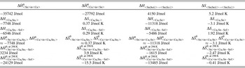
The thermodynamic parameters required for the calculation of (interface) energy values according to the expressions presented in Sec. III. A?III. D were obtained from both the experimental data (Table I) and theoretical calculation (Table II) by employing the quantitative thermodynamic models presented for the system Sn–Cu.Reference Liu, Wang, Ohnuma, Kainuma and Ishida43
Experimental data for some thermodynamic parameters for relevant phases in the system Sn–Cu taken from Refs. Reference Song, Tu and Lee45–Reference Wawra47.

aRef. Reference Song, Tu and Lee45, bRef. Reference Kittel46, cRef. Reference Wawra47.
V, molar volume; C Cu, atomic fraction of Cu; θ, Debye temperature; γs, surface energy (T in K). The notation “sol” refers to solid solution.
Theoretical data for thermodynamic parameters for the relevant phases in the system Sn–Cu.Reference Liu, Wang, Ohnuma, Kainuma and Ishida43

Note that the partial enthalpies and entropies of mixing of Cu and Sn in both considered solid solutions (Cu6Sn5–Sol and Cu3Sn–Sol) hold for T = 298 K. The notation “sol” refers to solid solution.
The Gibbs energies of formation of the IMCs Cu6Sn5 (η′) and Cu3Sn (ε) are expressed as


with T in K.
The Gibbs energy of the formation of a Cu–Sn solid solution phase with a face-centered cubic (fcc) structure is given as

with the excess molar Gibbs energy,  , given by

with T in K and c<i> as atomic fraction of the component i in Cu–Sn solid solution.
To account for the body-centered tetragonal (bct) structure of Sn, the Gibbs energy difference pertaining to the bct–fcc transformation can be accommodated usingReference Dinsdale44:

with T in K.
F. Critical thickness for phase formation
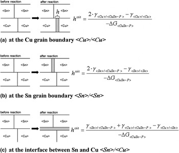
For the system (polycrystalline) Sn layer on (polycrystalline) Cu substrate, three potential sites for the formation of Cu6Sn5 and Cu3Sn (both as IMC and as solid solution) were considered in the present study, as shown schematically in Fig. 1: (a) at a Cu grain boundary <Cu>/<Cu>, (b) at a Sn grain boundary <Sn>/<Sn>, and (c) at the interface between Sn and Cu <Cu>/<Sn>. At each of these sites, the formation of a new phase is associated with the replacement of an interface (grain boundary) with two new interfaces, which can be accompanied with a decrease or an increase in total interfacial energy. If the total interface energy increases due to such phase formation (i.e., 2 × γ <new interface> − γ <old interface> > 0; this inequality holds for the cases considered here, see Fig. 7), a critical thickness h crit (i.e., a critical width for the “slabs” shown in Fig. 1) can be calculated which indicates the minimal thickness of the product phase <CuSn-P> needed to compensate the increase in total interface energy by the (bulk) energy released by <CuSn-P> formation. Beyond this critical thickness h crit, <CuSn-P> formation is energetically favored. Thus, a comparison of the critical thickness values calculated for different <CuSn-P> phases forming at a specific site allows the determination of the phase which thermodynamically will preferably form at this site.
Different possible sites for CuSn-phase (<CuSn-P>; i.e., Cu6Sn5 and Cu3Sn, as solid solution and as compound phase) formation in the system (polycrystalline) Sn on (polycrystalline) Cu; (a) at the Cu grain boundary <Cu>/<Cu>; (b) at the Sn grain boundary <Sn>/<Sn>; and (c) at the interface between Sn and Cu <Cu>/<Sn>. The corresponding equations for the calculation of the critical thicknesses h crit, beyond which the CuSn-phase considered is stable, have been plotted on the right-hand side. Note that ΔG <CuSn-P> in these equations should be expressed as energy per unit volume (see text).

Note that the equations given for h crit in Fig. 1 imply that the Gibbs energy of formation for <CuSn-P> should be expressed as energies per unit volume, whereas the equations and data given in Sec. III. A?III. E refer to energies per mol; the molar volumes for the corresponding conversion have been given in Table I.
IV. RESULTS AND DISCUSSION
A. Microstructural investigation of Sn/Cu specimens
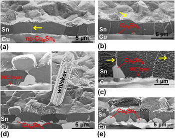
The microstructural evolution of polycrystalline Sn thin films ({321}-fiber texture, layer thickness of about 3 μm and in-plane grain sizes of 2–5 μm) with a columnar grain morphology electrodeposited on polycrystalline Cu substrates (see for further details Ref. Reference Sobiech, Welzel, Schuster, Mittemeijer, Hügel, Seekamp and Müller21) was investigated in detail during aging at room temperature (i.e., ∼25 °C) by employing FIB-based microscopy [FIB machining of Sn on Cu systems induces artifacts in the Sn microstructure. During high-energetic Ga+ ion beam cutting through the Sn on Cu system (e.g., to prepare cross-sections of the bilayer system), Cu atoms are removed from the substrate due to sputtering. Once the ion beam is switched off, Cu atoms from the gas phase react with the freshly prepared Sn surface, preferentially along Sn grain boundaries (as energetically preferred nucleation sites; see results of thermodynamic calculations performed in the present work and presented in Sec. IV. B. 2), and thus form Sn–Cu intermetallics.Reference Osenbach, DeLucca, Potteiger, Amin, Shook and Baiocchi48 Therefore, cross-sectional FIB micrographs of Sn layers on Cu exhibit typically bright Sn grain boundaries (due to significant formation of Sn–Cu intermetallics with a “line-like” morphology) as well as bright spots on the Sn grains due to the presence of fine Sn–Cu intermetallics, which are not formed under (undisturbed) aging conditions. This could be shown unequivocally by preparing FIB cuts which did not extend to the Cu substrate, that is, in such a case the Sn grain boundaries in the exposed section of the Sn layer were completely free of any Sn–Cu intermetallics.] (Figs. 2–4). In addition, detailed TEM analyses of the microstructure at and around a whisker nucleation site (Fig. 5) and x-ray diffraction phase analyses (Fig. 6) were conducted. Here, the focal point of interest was on the formation and growth of intermetallic phases during room temperature aging.
Focused ion beam (FIB) cross-sectional micrographs of Sn/Cu specimens taken after different aging times at room temperature: (a) Fresh (i.e., ∼1 h after Sn deposition); (b) ∼5 days; (c) ∼ 10 days; (d) ∼30 days; (e) ∼300 days. The intermetallic compound, Cu6Sn5 (IMC), formed during room temperature aging, has been indicated in the figure. The bright phase decorating the Sn grain boundaries as well as the Sn surface (see arrows) represents IMC formed as artifact due to FIB cutting (Sec. IV. A).

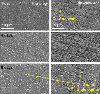
FIB micrographs taken after different aging times at room temperature (in top- and tilt-view) from specimens where the Sn layer was stripped off selectively (see Sec. II). Thus, the growth behavior of Cu6Sn5 at the Sn/Cu interface can be revealed: Cu6Sn5 forms preferentially along Sn grain boundaries, most pronouncedly at Sn grain boundary/interface triple junctions.

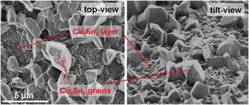
FIB micrographs (top- and tilt-view) taken from a specimen where the Sn coating was stripped off selectively after about 300 days of room temperature aging (see Sec. II), showing the morphology of Cu6Sn5 formed at the Sn/Cu interface.

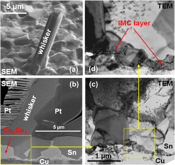
Side-view and cross-sectional micrographs of a Sn whisker of a Sn/Cu specimen taken after an aging time of several weeks at room temperature. (a) SEM side-view. (b) SEM cross-sectional micrograph of the FIB-prepared lamella used for TEM analysis. The Pt-layer was deposited prior to FIB-milling to protect the specimen surface. (c) Bright field cross-sectional TEM micrograph taken from the region marked in yellow in (b). (d) Bright field cross-sectional TEM micrograph, enhanced magnification of the region marked in yellow in (c).

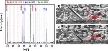
(Left) X-ray diffraction pattern (Cu Kα radiation) of a Sn thin film (thickness of about 1 μm) electrodeposited on Cu, recorded after an aging time at room temperature of about 2 years. Apart from diffraction lines belonging to Sn and Cu, the presence of diffraction lines of only Cu6Sn5 is detectable (the three most intensive reflections of Cu6Sn5 have been indexed in the figure). The PDF-files used for phase analysis have been indicated on top of the figure. (Right) FIB cross-sectional micrographs, taken shortly after diffraction analysis, through the Sn thin film aged for about 2 years: Cu6Sn5 had penetrated through the whole Sn layer of thickness of about 1 μm (see isolated remnants of Sn).

The experimental findings lead to the following time-resolved picture of the microstructural development during room temperature aging:
(i) Directly after Sn deposition, that is, after an aging time of roughly 1 h, no significant intermetallic phase formation has taken place [Fig. 2(a)]. It was reported on the basis of atomic forceReference Zhang, Egli, Schwager and Brown29 and TEMReference Kumar, Reinbold, Bower and Chason20 analyses, that already 1 h aging after Sn deposition suffices to generate very fine-grained intermetallic particles at the Sn/Cu interface. At this aging time, that is, before the onset of significant intermetallic phase growth, the Sn/Cu specimen is still free of hillocks and whiskers.
(ii) Upon continued aging at room temperature, a significant amount of the intermetallic phase Cu6Sn5 [Fig. 6; also verified by energy dispersive x-ray analyses (data not shown)] forms on the Sn side of the Sn/Cu interface, which extends only into the Sn (i.e., no intermetallic phase formation occurred on the Cu side). These findings, which agree with the results reported in Ref. Reference Kumar, Reinbold, Bower and Chason20, were confirmed by time-resolved FIB and x-ray diffraction phase analyses performed in this work for aging periods up to 2 years (Fig. 6). (For this purpose, specimens with a Sn layer thickness of only about 1 μm were used to obtain pronounced diffraction information of the growing intermetallic phase.)
(iii) Initially, Cu6Sn5 formation occurs predominantly at the intersections of the Sn grain boundaries with the Sn/Cu interface (Figs. 2 and 3). Upon continued aging Cu6Sn5 growth proceeds significantly into the Sn coating along the Sn grain boundaries accompanied by lateral (i.e., in directions parallel to the Sn/Cu interface) growth (Figs. 2–4). Pronounced Cu6Sn5 growth takes place particularly at triple junctions of Sn grain boundaries (Fig. 3). As evident from the bright-field TEM micrograph shown in Fig. 5(c), Cu6Sn5 forming along Sn grain boundaries grows as a single crystal (see also the idiomorphic surface morphology of Cu6Sn5 in tilt-view, Fig. 4).
The Sn-layer penetrating growth morphology of Cu6Sn5 is responsible for the development of residual compressive stress parallel to the Sn/Cu interface, in the Sn coating,Reference Sobiech, Welzel, Schuster, Mittemeijer, Hügel, Seekamp and Müller21 and roughly 4 days after Sn deposition (for the investigated Sn/Cu specimens) whisker formation on the surface of the Sn coating occurs.
(iv) Upon prolonged aging at room temperature, Cu6Sn5 formation commenced also on the Sn side of the Sn/Cu interface, that is, on the faces of the Sn grains adjacent to the Sn/Cu interface [Fig. 2(c)], but with an extent (i.e., penetration of the Sn grains) much less than those for the Cu6Sn5 formation along the Sn grain boundaries, as described above. This Cu6Sn5 layer is composed of fine-grained, rather columnar Cu6Sn5 grains [Figs. 4 and 5(d)].
(v) The location of a whisker root at the surface of the Sn layer always coincided with particularly pronounced Cu6Sn5 formation at the Sn/Cu interface at the same lateral positions [Figs. 2(d) and 5(b)].
(vi) Apart from the formation of Cu6Sn5 in the Sn layer and the growth of Sn whiskers out of the Sn layer, the Sn microstructure remained unchanged during aging.
B. Interface thermodynamic calculations for the system Sn on Cu
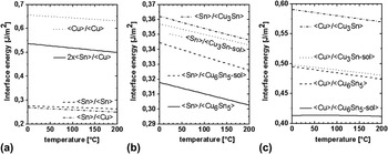
By employing the treatment for interface thermodynamics described in Sec. III. A?III. E, the interface energies of all relevant material combinations (i.e., <Cu>/<Cu>, <Sn>/<Sn>, <Sn>/<Cu>, <Cu>/<CuSn-P>, and <Sn>/<CuSn-P>) were calculated for the temperature range of 0–200 °C (Fig. 7). It follows that CuSn-phase formation at the interfaces is counteracted by the associated formation of new interfaces (i.e., 2·γ <Me>/<CuSn-P>−γ <Me>/<Me> > 0) and as a consequence a critical thickness for CuSn-phase formation can be calculated (Sec. III. F). The corresponding results will be discussed next.
Interface energies for all relevant material combinations as a function of temperature: (a) interfaces between the pure metals <Sn> and <Cu>; (b) interfaces between <Sn> and the CuSn phases Cu3Sn and Cu6Sn5 (as solid solution and as compound); and (c) interfaces between <Cu> and the CuSn phases Cu3Sn and Cu6Sn5 (as solid solution and as compound).

1. Kinetic constraints for the formation of Cu3Sn versus Cu6Sn5
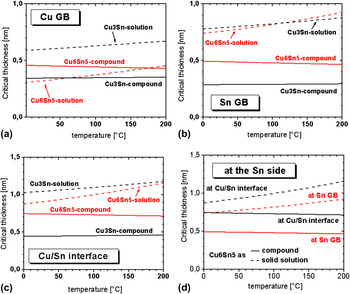
The calculated critical thicknesses h crit for the formation of Cu6Sn5 and Cu3Sn [either as solid solution or as compound) at a <Cu> grain boundary, a <Sn> grain boundary, and the <Sn>/<Cu> interface are shown as a function of temperature in Figs. 8(a)–8(c)].
Critical thicknesses for CuSn-phase (i.e., Cu6Sn5 and Cu3Sn, either as solid solution or as compound) formation at (a) a <Cu> grain boundary; (b) a <Sn> grain boundary; and (c) the interface between <Sn> and <Cu>. In (d) the critical thicknesses for the formation of Cu6Sn5 at the <Sn> side of the <Sn>/<Cu> interface are shown; this figure is a summary of the results shown in (b) and (c).

As a general, first, result, it follows that from a thermodynamic point of view the formation of Cu3Sn is favored over the formation of Cu6Sn5, no matter which site (grain boundary or interface) for phase formation is considered. However, the experimental results (Sec. IV. A) indicate that during aging at room temperature only Cu6Sn5 formation is observed. This discrepancy has a simple kinetic background: (i) at each position at the <Sn> side, upon inward diffusion of Cu, the stoichiometric composition needed for Cu6Sn5 formation will always be reached prior to the stoichiometric composition compatible with the formation of Cu3Sn, and (ii) the formation of Cu3Sn at the <Cu> side is impossible at room temperature because the diffusion of Sn in Cu at room temperature is negligible.Reference Tu6, Reference Dyson, Anthony and Turnbull26, Reference Tu and Thompson28 Therefore, in the following discussion, only the critical thicknesses for the formation of Cu6Sn5 at different sites in the microstructure at the <Sn> side will be considered.
2. Critical thicknesses for the formation of Cu6Sn5 at the Sn side of the Sn/Cu interface
The comparison of the critical thicknesses for nucleation of Cu6Sn5 at each possible nucleation site at the <Sn> side [Fig. 8(d)] reveals that the Cu6Sn5 formation as (ordered) compound is energetically preferred compared to its (disordered) solid solution state, that is, Cu6Sn5 IMC formation will occur directly without passing a (metastable) solid solution state.
The critical thickness for the formation of Cu6Sn5 as IMC at room temperature is lowest at <Sn> grain boundaries (∼0.5 nm), followed by the <Sn>/<Cu> interface (∼0.75 nm). Hence, Cu6Sn5 IMC formation along <Sn> grain boundaries is thermodynamically most preferred. This prediction is in very good agreement with the experimental observations (Sec. IV. A), which showed that Cu6Sn5 compound formation indeed occurs initially along <Sn> grain boundaries intersecting the <Sn>/<Cu> interface.
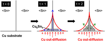
Upon continued aging at room temperature, IMC formation does not proceed only along <Sn> grain boundaries until reaching the <Sn> layer surface. Diffusion of Cu in <Sn> grain boundaries is much faster than that of volume, bulk diffusion of Cu in Sn. This, together with the relatively low value for the critical thickness at this location, causes Cu6Sn5 to form first at <Sn> grain boundaries. [The increased diffusion of Cu along the <Sn> grain boundary intersecting the <Sn/Cu> interface governs the (morphology of the) formation and distribution of Cu6Sn5 in the Sn layer. This is compatible with observations that electrodeposited Sn layers containing co-deposited Cu exhibit significant, initial Cu6Sn5 formation only along <Sn> grain boundaries (i.e., in the form of “isolated” precipitates distributed over the <Sn> grain-boundaries), independent of the substrate material used (e.g., CuReference Boettinger, Johnson, Bendersky, Moon, Williams and Stafford16, Reference Sheng, Hu, Choi, Tu, Bong and Nguyen49 or WReference Williams, Moon, Boettinger, Josell and Deal50), as in this case the Sn layer itself serves as source for Cu atoms.] The formation of Cu6Sn5 at the <Sn>/<Cu> interface requires the transport of Cu by volume diffusion. This, together with the relatively large value for the critical thickness at this (thus less preferred) location, causes Cu6Sn5 to form at a later stage at the <Sn>/<Cu> interface (at the <Sn> side). Obviously, Cu enrichment by volume diffusion of Cu is most pronounced close to <Sn> grain boundaries intersecting the <Sn>/<Cu> interface (Fig. 9): Cu arrives at this location by volume diffusion both from the substrate and from the <Sn> grain boundaries. Only after several days of aging at room temperature Cu6Sn5 formation can also occur along the <Sn>/<Cu> interface remote from locations where <Sn> grain boundaries intersect the <Sn>/<Cu> interface. [Heterogeneous nucleation of Cu6Sn5 and subsequent “island” coalescences lead to the formation of a polycrystalline, closed and rather planar layer of Cu6Sn5 at the <Sn/Cu> interface, as revealed by FIB and TEM analyses (Figs. 2 and 5). This closed layer of Cu6Sn5 acts during further aging at room temperature as diffusion barrier for Cu and thus further (“regular”) growth of Cu6Sn5 proceeds significantly slower as compared to further (“irregular”) growth of Cu6Sn5 along <Sn> grain boundaries intersecting the <Sn/Cu> interface, as observed.] Thus, the development of the irregular growth morphology of Cu6Sn5 can be understood.
Continued growth of the Cu6Sn5, originally formed at the <Sn> grain boundaries intersecting the <Sn>/<Cu> interface, could occur in particular in “diagonal” directions (see green arrows in Fig. 9), to minimize the total interface energy of the system upon grain growth.
Schematic illustration of Cu diffusion and Cu6Sn5 formation processes during room temperature aging (for successive aging time steps t = 0, 1, and 2) at a <Sn> grain boundary intersecting the <Sn>/<Cu> interface, leading to the formation of Cu6Sn5 with an irregular growth morphology. The red, solid line illustrates a Cu iso-concentration profile in the Sn phase. The vertical blue arrow denotes grain-boundary diffusion of Cu along the <Sn> grain boundary: the horizontal blue arrows denote volume-diffusion of Cu originating from the <Sn> grain boundary (further see text).

The above discussion provides an explanation for the morphology and distribution of the developing Cu6Sn5 phase in the Sn layer as the outcome of both thermodynamic and kinetic arguments.
V. WHISKER MITIGATION BY APPLICATION OF INTERFACE THERMODYNAMICS
The origin for Sn whisker formation in the system Sn on Cu has recently been ascribed to the development of stress gradients, parallel and perpendicular to the Sn/Cu interface, in the Sn layer as a consequence of the formation of Cu6Sn5 with an irregular growth morphology (Sec. IV. A).Reference Sobiech, Welzel, Mittemeijer, Hügel and Seekamp22, Reference Sobiech, Wohlschlögel, Welzel, Mittemeijer, Hügel, Seekamp, Liu and Ice23 On the basis of the treatment presented in this paper (see, in particular, Sec. IV. B), the following whisker mitigation treatment can now be proposed.
During aging at room temperature the occurrence of residual stress gradients, especially close to Sn grain boundaries, is caused by the laterally inhomogeneous development of Cu6Sn5, penetrating deeply into the Sn layer from the Sn/Cu interface, along Sn grain boundaries intersecting the Sn/Cu interface. Such gradients would not develop such pronouncedly if a layer-like, planar growth of Cu6Sn5 along the entire Sn/Cu interface into the Sn layer would develop. In view of the results presented in Sec. IV. B (Fig. 8), the formation of planar Cu6Sn5 along the Sn/Cu interface could be achieved if the critical thickness for the formation of Cu6Sn5 along the Sn/Cu interface becomes lower than that for the formation of Cu6Sn5 along Sn grain boundaries, that is, the layer/substrate interface energy must be increased and/or the Sn grain-boundary energy must be decreased. Moreover, a (laterally) closed, planar layer of Cu6Sn5 forming along the Sn/Cu interface acts as diffusion barrier for Cu from the substrate into the Sn coating which decelerates continued intermetallic phase formation in the Sn coating upon continued aging at room temperature.
The above discussion sheds light on the (well-known; see Refs. Reference Zhang and Schwager30, Reference Arnold51) whisker-mitigating effect of Pb: incorporation of Pb into the Sn upon deposition on Cu changes, during subsequent aging, the growth morphology of Cu6Sn5 to the desired, planar one,Reference Zhang and Schwager30, Reference Sobiech, Teufel, Welzel, Mittemeijer and Hügel52 and indeed a Pb-content of even a few wt% suffices to prevent effectively the whisker formation.Reference Arnold51 It is very likely that the presence of Pb drastically reduces the Sn grain-boundary energy: wetting of Sn grain boundaries by Pb leads to Sn/Pb interfaces of energy about half of that of Sn/Sn interfaces (i.e., Sn grain boundaries).Reference Gupta, Vieregge and Gust53 Hence, the incorporation of Pb in the Sn layer in fact implies the application of interface thermodynamics to obstruct whisker formation. This interpretation is also compatible with recent investigations of the whiskering behavior of Sn–Pb coatings, which revealed the absence of whiskering, also in columnar Sn–Pb coatings (in accordance with the above discussion),Reference Sobiech, Teufel, Welzel, Mittemeijer and Hügel52 whereas previous work suggested that the whisker-mitigating effect of Pb is due to the occurrence of an equiaxed microstructure in Sn–Pb coatings.Reference Boettinger, Johnson, Bendersky, Moon, Williams and Stafford16
This thermodynamic approach to whisker mitigation provides a pathway for identifying elements to be incorporated in the Sn coating and which trigger a planar Cu6Sn5 growth morphology and which elements do not impose environmental concerns as Pb does.
VI. CONCLUSIONS
(1) According to “bulk” thermodynamics, reaction in a Sn/Cu system can lead to the formation of the IMCs Cu3Sn and Cu6Sn5. Interface thermodynamics, recognizing the cost of IMC/metal interface formation, allows both the formation of Cu3Sn and Cu6Sn5 at interfaces and grain boundaries, but favors the formation of Cu3Sn at Sn grain boundaries, Cu grain boundaries, and at the Sn/Cu interface.
(2) At room temperature significant diffusion of Cu into Sn can occur, but the diffusion of Sn into Cu is negligible. As a consequence, Cu3Sn formation does not occur initially (at the Cu-side). Instead, at the Sn side of the Sn/Cu system Cu6Sn5 formation (the Sn-rich IMC) occurs. The absence of Cu3Sn at ambient temperature is thus a consequence of diffusion kinetics, and not of thermodynamics.
(3) Interface thermodynamics predict that Cu6Sn5 formation occurs preferentially at the Sn grain boundaries intersecting the Sn/Cu interface, as compared to along the Cu/Sn interface, which agrees with the experimental observations.
(4) Cu6Sn5 formation along the Sn/Cu interface is thermodynamically possible but less favored (larger critical thickness than for Cu6Sn5 formation along Sn grain boundaries) and can only be realized by volume diffusion of Cu and therefore is observed only after prolonged aging.
(5) The irregular growth morphology associated with the formation of Cu6Sn5 penetrating the Sn layer leads to pronounced lateral and vertical residual stress gradients in the Sn layer, especially close to Sn grain boundaries used for Cu6Sn5 formation, thereby driving whisker formation. The concept of interface thermodynamics, presented in this paper, can be used to promote planar growth of closed Cu6Sn5 layers, that is, to favor IMC formation at the Sn/Cu interface, for example by incorporation of a component in Sn that reduces the Sn grain-boundary energy. Thereby, development of residual stress gradients in the Sn layer, which can cause whiskering, is avoided.
(6) The whisker-mitigating effect of Pb can now, for the first time, be rationalized on the basis of interface thermodynamics: wetting of Sn grain boundaries by Pb changes, during subsequent aging, the growth morphology of Cu6Sn5 to the desired, planar one.
ACKNOWLEDGMENTS
The authors are much obliged to the company “Hans Heimerdinger Oberflächentechnik” in Pforzheim, Germany for specimen preparation. The authors would also like to thank Mrs Ulrike Eigenthaler (Max Planck Institute for Metals Research, Stuttgart) for preparing cross-sectional lamellae, by means of FIB, suitable for TEM analysis and Dr. Ewald Bischoff (Max Planck Institute for Metals Research, Stuttgart) for performing the TEM investigations.