I. INTRODUCTION
Quantum computing has been one of the most exciting developments in modern computational technologies and can potentially revolutionize our ways of information processing and communication. The field is actively searching for novel platforms capable of achieving the eventual scaling up. Majorana fermion-based topological quantum computing is one of the most promising candidates. Majorana fermions, which are a type of nonabelian anyons, are able to carry out error-tolerant topological quantum computing.Reference Ivanov1,Reference Catherine2 In conventional p-wave superconductors, electrons form spin triplet Cooper pairs with spinless nature and perfect particle-hole symmetry. Majorana zero-modes can be trapped inside superconductor vortex cores. However, intrinsic p-wave superconductors are rare and fragile in thin films due to broken time-reversal-symmetry in the pairing, thus unlikely to be applicable in practical devices.Reference Ando and Fu3–Reference Sau, Lutchyn, Tewari and Sarma5 Therefore, simulating p-wave superconductors through proximity effect has become a more attractive approach. Recently, signatures of Majorana fermions on semiconductor nanowires with strong Rashba spin–orbit coupling have been reported.Reference Zhang, Liu, Qi, Dai, Fang and Zhang6,Reference Chen, Analytis, Chu, Liu, Mo, Qi, Zhang, Lu, Dai, Fang, Zhang, Fisher, Hussain and Shen7 Such a nanowire approach does however suffer significantly in terms of scalability further down the path. Topological insulators (TIs), a type of newly discovered quantum materials, provide another viable platform. TIs possess robust, topologically protected surface states on their boundaries/interfaces with other topologically trivial materials. These conducting surface states are formed with helical Dirac fermions, with their spin and momentum strictly locked by intrinsic spin–orbit coupling.Reference Xia, Qian, Hsieh, Wray, Pal, Lin, Bansil, Grauer, Hor, Cava and Hasan8–Reference Kitaev11 It was predicted in a recent research study that a p-wave-like superconducting state can be induced by the proximity effect at the interface between a TI and a conventional s-wave superconductor, which can then readily host Majorana fermions.Reference Nayak, Simon, Stern, Freedman and Sarma12 Several groups have succeeded in observing coexisting superconductivity and topological surface states in different kinds of superconductor/TI heterostructuresReference Wang, Liu, Xu, Yang, Miao, Yao, Gao, Shen, Ma, Chen, Xu, Liu, Zhang, Qian, Jia and Xue13–Reference Sun, Zhang, Hu, Li, Wang, Ma, Xu, Gao, Guan, Li, Liu, Qian, Zhou, Fu, Li, Zhang and Jia16 by scanning tunneling spectroscopy (STM), angle-resolved photoelectron spectroscopy,Reference Xu, Alidoust, Belopolski, Richardella, Liu, Neupane, Bian, Huang, Sankar, Fang, Dellabetta, Dai, Li, Gilbert, Chou, Samarth and Hasan17 and transport measurement.Reference Zareapour, Hayat, Zhao, Kreshchuk, Jain, Kwok, Lee, Cheong, Xu, Yang, Gu, Jia, Cava and Burch18 TI films have been grown on NbSe2, Bi2Ca2Cu2O8+δ,Reference Wang, Liu, Xu, Yang, Miao, Yao, Gao, Shen, Ma, Chen, Xu, Liu, Zhang, Qian, Jia and Xue13,Reference Wang, Ding, Fedorov, Yao, Li, Lv, Zhao, Zhang, Xu, Schneeloch, Zhong, Ji, Wang, He, Ma, Gu, Yao, Xue, Chen and Zhou19 and NbN substrates.Reference Koren and Kirzhner20–Reference Koren23 Recently, chiral Majorana fermion modes were found on TIs in contact with Nb electrodes.Reference He, Pan, Stern, Burks, Che, Yin, Wang, Lian, Zhou, Choi, Murata, Kou, Chen, Nie, Shao, Fan, Zhang, Liu, Xia and Wang24 In recent years, TI/superconductor Josephson junctionsReference Williams, Bestwick, Gallagher, Hong, Cui, Bleich, Analytis, Fisher and Gordon25–Reference Pang, Wang, Lyu, Yang, Fan, Liu, Ji, Jing, Yang and Lu28 have attracted great attention in condensed matter physics, with most of them being in-plane junctions. Now, we are aiming at a step further to create high-quality superconductor/TI/superconductor vertical Josephson junctions to track down Majorana modes on the ends of penetrating flux lines.Reference Chiu, Gilbert and Hughes29 TI vertical junctions have potential applications in spintronicsReference Fan, Upadhyaya, Kou, Lang, Takei, Wang, Tang, He, Chang, Montazeri, Yu, Jiang, Nie, Schwartz, Tserkovnyak and Wang30,Reference Kou, He, Lang, Fan, Wong, Jiang, Nie, Jiang, Upadhyaya, Xing, Wang, Xiu, Schwartz and Wang31 and superconductor electronicsReference Chiu, Gilbert and Hughes29 due to the access to both the top and bottom topological surface states. Compared with lateral junctions, vertical Josephson junctions with thinner TI films could better maintain superconducting coherence. Furthermore, controlling the thickness of TIs would modify the coupling and superconducting coherence between the top and bottom surface states.Reference Zhang, He, Chang, Song, Wang, Chen, Jia, Fang, Dai, Shan, Shen, Niu, Qi, Zhang, Ma and Xue32 It is highly desirable to maintain good interface qualities for these purposes. However, vertical junctions and heterostructures are very hard to fabricate and full of challenges, especially for high-quality materials growth compatible with the desired electrode materials and subsequent quality-preserved device fabrication processes. Not only optimizing the quality of the topological materials themselves is critical but also the electrode materials as well as the interfaces should be kept in pristine conditions. In this work, we made a series of experiments using highly textured Nb films as the bottom electrode material and depositing high-quality (Bi0.5Sb0.5)2Te3 in an epitaxial form. More importantly, we developed a two-step growth method to promote efficient nucleation of (Bi0.5Sb0.5)2Te3 films on Nb surfaces, while under the same conditions, direct deposition leads to amorphous-like film growth. This is because in one-step depositions, the excess Te and the high temperature favor strong chemical reactions leading to foreign phases and break the epitaxy. In the two-step method, Bi, Sb, and Te clusters were deposited by physical absorptions at a temperature of 180 °C, lower than the normal growth temperature, then a proper annealing process helps forming a crystallization passivation layer through solid-state epitaxy without inducing much chemical reactions. Therefore, we are able to obtain clean interfaces and good epitaxial passivation. (Bi0.5Sb0.5)2Te3 films in the second step were deposited on the passivation layer at the normal growth temperature. We further present vertical TI Josephson junctions with good IV characteristics, demonstrating the validation of our growth methods.
II. EXPERIMENTAL PROCEDURE
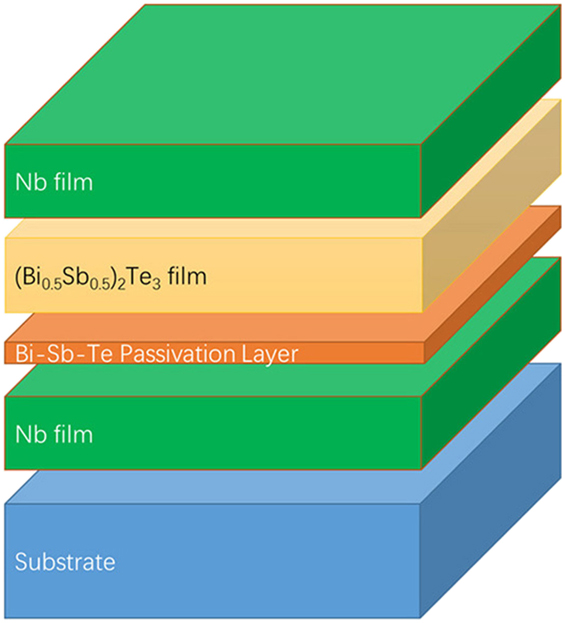
Substrate surfaces’ cleanliness is critical for molecular beam epitaxy (MBE), as any surface disorder or contamination would lead to crystal defects and secondary phases in the epitaxial layers.Reference Zhang, He, Chang, Song, Wang, Chen, Jia, Fang, Dai, Shan, Shen, Niu, Qi, Zhang, Ma and Xue32 In our experiment, the TIs and superconductors were deposited in separate chambers of an ultra-high vacuum (UHV) clustered deposition system (Omicron NanoTechnology GmbH, Taunusstein, Germany), and the substrates were in situ transferred from one chamber to another to maintain clean and well-defined interfaces between layers. The finial Nb/(Bi0.5Sb0.5)2Te3/Nb heterostructure is illustrated in Fig. 1. We used MBE growth for the TI films (Bi0.5Sb0.5)2Te3. We choose this ternary TI such that the Dirac points can be tuned to within the band gap by varying the Sb ratio in this material. Magnetron sputtering was used for the superconductor Nb films. The superconductor material can also be replaced by NbN films. The base pressures of the deposition chambers and the transfer line are better be 5 × 10⁻¹⁰ mbar.
Illustration of the Nb/(Bi0.5Sb0.5)2Te3/Nb heterostructure.

The heterostructure deposition procedure follows several steps. First, the sapphire (0001) substrate was mounted on a holder and physically bombarded with radio frequency Ar sputtering to eliminate contamination on the surface. Second, it was annealed at 700 °C in UHV to recrystallize the surface. The reflection high-energy electron diffraction (RHEED) pattern clearly showed a streaky pattern indicating a well-structured and smooth surface. The substrate was then in situ transferred to a magnetron-sputtering chamber to deposit the Nb film. In our experiment, Nb films were used as the electrodes in vertical Josephson junctions because they offer great stability and compatibility with the subsequent micro/nanofabrication procedures. Similar high-quality Nb film deposition was reported previously.Reference Tang, Zhang, Kwon, Mohebbi, Cory, Peng, Gu, Guo, Jin and Miao34 Nb sputtering was performed under 30 sccm of Ar gas flow and a DC power of 200 W. The base pressure of the chamber was lower than 5 × 10⁻¹⁰ mbar to keep the chamber clean, thus reducing unwanted compounds such as Nb oxides. For NbN film deposition, an additional 2 sccm N2 gas was introduced close to the substrate for reactive sputtering.
Immediately after the bottom superconductor film was prepared, the sample was transferred in situ to the MBE chamber for the (Bi0.5Sb0.5)2Te3 film deposition. High-purity Bi (99.997%) and Sb (99.999%) were co-evaporated from Knudsen cells, and Te (99.99%) was evaporated from a thermal cracker source. Quartz microbalance monitor and beam flux monitor were independently used to calibrate the fluxes beforehand. The entire process was carried out with the flux ratio of Bi/Sb and Te set to 1:10Reference Zhang, Chang, Zhang, Wen, Feng, Li, Liu, He, Wang, Chen, Xue, Ma and Wang33 and the growth rate of the (Bi0.5Sb0.5)2Te3 thin film was controlled at 0.3 nm per minute.
The crystalline quality of the (Bi0.5Sb0.5)2Te3 and Nb thin films were characterized by X-ray diffraction (XRD, with Bruker D8 Advance, Bruker Corporation, Madison, Wisconsin) with Cu Kα radiation (λ = 1.54 Å). The chemical stoichiometry of the (Bi0.5Sb0.5)2Te3 thin films were characterized by X-ray photoelectron spectroscopy (XPS, with Mg Kα source and Omicron Argus 128 channel analyzer, Omicron NanoTechnology GmbH, Taunusstein, Germany). The binding energies in the XPS analysis were standardized by the C 1s peak at 284.6 eV. We further applied atomic force microscopy (AFM, with Veeco Innova, Plainview, New York) to investigate the morphology of the Nb and (Bi0.5Sb0.5)2Te3 surfaces. Scanning tunneling microscopy (STM, with Omicron STM, Taunusstein, Germany) was carried out to obtain atomic resolution surface imaging. High resolution transmission electron microscopy (HRTEM) was performed to further check the structural and interfacial quality of the heterostructures, respectively.
After the (Bi0.5Sb0.5)2Te3 film deposition was done, the sample was transferred back to the sputtering chamber and the top Nb layer was deposited under the same experimental conditions as the bottom Nb deposition. 10 nm Ti and 5 nm Au were then placed as a capping layer to protect the films. The heterostructure was next fabricated into micron-sized vertical Josephson junctions using standard photolithography and ion milling techniques. Josephson current measurements were performed with 4-terminal method in a continuous flow cryostat at 2–7 K temperatures.
III. EXPERIMENTAL RESULTS AND DISCUSSION
A. (Bi0.5Sb0.5)2Te3 film deposition on different substrates
The clear RHEED pattern of a deposited 50 nm Nb film on the sapphire (0001) substrate and the ex situ off-axis XRD scans both indicate a highly textured (110)-Nb film growth. We found that three equivalent in-plane layouts are simultaneously present on the hexagonal sapphire lattice, i.e., three ways of stacking a rectangular (110)-Nb atomic layer onto a hexagonal (0001)-sapphire atom layer. The roughness of the Nb surface was less than 0.5 nm characterized by AFM. We then attempted to directly deposit (Bi0.5Sb0.5)2Te3 on top. Usually growing (Bi0.5Sb0.5)2Te3 films on sapphire (0001) and SrTiO3(111) substrates, the deposition temperature is in the range of 220–300 °C, with 280 °C yielding the best transport properties. RHEED clearly showed streaky patterns and layer-by-layer intensity oscillations, which means crystalline compound appeared on the substrates. When the substrate temperature is lower than 220 °C, the RHEED pattern shows the formation of particles and nanostrips on the surface. On the other hand, at temperatures higher than 300 °C, there appears no pattern of TI films, only patterns from the substrate. We also attempted to deposit (Bi0.5Sb0.5)2Te3 films on the Nb substrate at 280 °C directly, but RHEED patterns did not show any crystalline structures either, only amorphous structures [Supplementary Material Fig. S2(b)]. The surface of the directly deposited film also showed clusters from AFM. We attempted a series of Nb substrate temperatures from 200–300 °C to directly deposit (Bi0.5Sb0.5)2Te3 films. However, RHEED patterns only revealed amorphous-like film growth. We also checked the influence of the (Bi0.5Sb0.5)2Te3 films deposition rates tuned from 0.1 quintuple layers (QLs)/per minute to 5 QLs/per minute. In spite of the various deposition rates attempted, RHEED patterns still revealed amorphous-like film growth suggesting improper (Bi0.5Sb0.5)2Te3 nucleation directly on the Nb surface with the one-step direct deposition.
In some typical MBE growth processes, poor quality film deposition happened due to poor lattice matching between the film and substrate. Although it is expected that (Bi0.5Sb0.5)2Te3 and Nb have a fairly matched lattice constant and structure, our experiments showed that amorphous TIs still prevail on the Nb surface. However, it was demonstrated in the literature that even on SiO2 amorphous surfaces, TIs could achieve highly textured growth through Van der Waals epitaxy.Reference Jerng, Joo, Kim, Yoon, Lee, Kim, Kim, Yoon, Chuna and Kim35 Therefore, we believe that lattice mismatching is not the main reason for the amorphous-like (Bi0.5Sb0.5)2Te3 film deposition in our case. Some other factors are responsible for the failed epitaxial nucleation in the one-step (Bi0.5Sb0.5)2Te3 film deposition.
To find out the reason of the poor-quality deposition, we tried various substrates for (Bi0.5Sb0.5)2Te3 deposition, such as Al2O3(0001), SrTiO3(111), Si(111), textured EuS(111), and epi-MgO(111) on Si(111). The TI deposition quality was first evaluated by RHEED images as in Supplementary Material Fig. S1(a). From Supplementary Material Fig. S1(b), sharp RHEED streaky lines and intensity oscillation were observed for (Bi0.5Sb0.5)2Te3 deposited on Al2O3(0001), SrTiO3(111), and Si(111), which confirmed the desired layer-by-layer growth on these substrate surfaces. The intensity of RHEED pattern oscillation revealed different film deposition qualities, especially for the (Bi0.5Sb0.5)2Te3 deposited on the Si(111) substrate, the RHEED oscillation was very week and disappears with only 4 QL (Bi0.5Sb0.5)2Te3 deposited. RHEED patterns also showed different streaky line width indicating different film qualities, such as film roughness and particle sizes. These results were in good agreement with the AFM observations that the (Bi0.5Sb0.5)2Te3 deposited on SrTiO3(111) substrates showed the most smooth surfaces while some nonuniform (Bi0.5Sb0.5)2Te3 multiplayer islands were appearing on Si(111) substrates. It means the imperfect deposition quality on different substrates.
On the other hand, when (Bi0.5Sb0.5)2Te3 was deposited on MgO, Nb, and NbN surfaces, RHEED patterns always showed amorphous-like deposition. We tried various substrate temperatures and deposition rates, but amorphous growth still exists. These results clearly indicated that the quality of the (Bi0.5Sb0.5)2Te3 film depends sensitively on the substrates, and some mechanisms were blocking the nucleation in our desired heterostructures.
B. (Bi0.5Sb0.5)2Te3 film deposition on the Nb surface with two-step method
To inspect the interface between (Bi0.5Sb0.5)2Te3 and Nb, we deposited ultrathin (Bi0.5Sb0.5)2Te3 films directly on Nb surfaces at the regular growth temperature of 280 °C. The interface chemical environment of the ultrathin (Bi0.5Sb0.5)2Te3 film was measured using XPS in Supplementary Material Fig. S2(a). The ratio of Bi, Sb to Te is lower than 2:3 in these films. It turns out that the Te element is more concentrated compared to the desired (Bi0.5Sb0.5)2Te3 film, which means that direct deposition at 280 °C did not realize the stoichiometric (Bi0.5Sb0.5)2Te3 phase.
Typically, (Bi0.5Sb0.5)2Te3 films will break down when the substrate temperature is higher than 300 °C. From the RHEED patterns, we can observe that the streaky pattern of the film disappeared, and the substrate signal showed up, which means the TI indeed broke down during thermal annealing. However, we followed this method and annealed the one-step deposited amorphous film on Nb. The RHEED pattern changed from the amorphous pattern to the substrate crystal pattern when the substrate temperature increased higher than 800 °C. At this point, the amorphous pattern disappeared and the substrate pattern showed up, which indicates that in the one-step direct deposition process, the nucleated materials at 280 °C are not the TI material, but more mixed with NbTex phases. Therefore, the chemical property change in the one-step deposition might prevent the subsequent (Bi0.5Sb0.5)2Te3 film’s epitaxial nucleation on the Nb surface.
In previous reports, dangling bonds on certain surfaces, such as Si, act as chemically active sites for the adatoms and form secondary phases such as SiSe2, which create rough and disordered surfaces and block further material nucleation. Since Si dangling bonds can be saturated by depositing 0.3 or 1 monolayer Bi thin film and creating a  $\sqrt 3$ Bi terminated Si(111) surface, this was used in multilayer Bi depositionReference Bansal, Kim, Edrey, Brahlek, Horibe, Iida, Tanimura, Li, Feng, Lee, Gustafsson, Andrei and Oh36 and Bi shows good and orderly construction on Si(111) surfaces. On NbSe2 surfaces, the Bi terminated surface also assists the growth of TI films.Reference Wang, Liu, Xu, Yang, Miao, Yao, Gao, Shen, Ma, Chen, Xu, Liu, Zhang, Qian, Jia and Xue13 However, in our experiments, the Nb surface cannot effectively retain Bi atoms, which makes Bi atoms diffuse randomly on the surface. We tried various substrate temperatures to deposit and nucleate Bi atoms on the Nb surfaces, but only amorphous Bi films formed and blocked the ordered deposition of topological materials. Therefore the
 $\sqrt 3$ Bi reconstruction is not a feasible option on the Nb surfaces.
Besides the Bi reconstruction approach, depositing thin TI layers before the actual growth has also been well adopted.Reference Li, Wang, Kan, Guo, He, Wang, Wang, Wong, Wang and Xie37 In a relevant study, a thin Bi–Se film was first deposited at cryogenic temperature (∼100 K), and then the sample was annealed at the normal growth temperature to promote the formation of Bi2Se3 single crystals. This method effectively avoids the strong chemical interaction between the surface and first TI layer, which blocks the improper nucleation at the interface. The importance of this method is to achieve an amorphous film deposition at the beginning and then convert into crystal structure with annealing.
Following this method,Reference Jerng, Joo, Kim, Yoon, Lee, Kim, Kim, Yoon, Chuna and Kim35 we found that it still cannot effectively avoid the strong chemical interaction between the Nb surface and the first TI layer (especially between Nb and Te). For thinner (Bi0.5Sb0.5)2Te3 films (lower than 10 QLs), the strong interaction blocks the adatoms’ diffusion. The excess Te and the high annealing temperature favor strong chemical reactions leading to foreign phases in the material and break the film epitaxy. The big amorphous Bi–Sb–Te particulates change into large defects and textures after annealing. Thus no single crystal was formed during the annealing process. The bottom layers are not flat and not continuous and cannot fully cover the substrate. In the annealing process, the undesired particles continuously increase in size. We therefore propose a new kind of two-step method to fabricate a passivation layer that is thin, flat, more compact, and with good crystallization at the interface.Reference Jerng, Joo, Kim, Yoon, Lee, Kim, Kim, Yoon, Chuna and Kim35 One can expect that this layer is used to saturate the surface chemical sites and effectively blocks the TI’s direct chemical contact with the substrate.
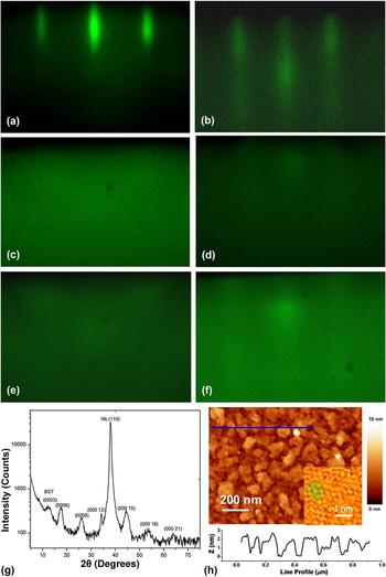
In our two-step deposition, when the surface temperature is nearly 180 °C, Bi, Sb, and Te start to condense into clusters and particles. The RHEED pattern shows small weak specular spots and streaky diffraction patterns [Fig. 2(b)]. When we continued to deposit Bi, Sb, and Te materials at this temperature, the RHEED pattern gradually disappears and becomes dark, which means that the Bi, Sb, and Te passivation layers can only form one monolayer’s crystalline structure at this low temperature.
RHEED patterns for the (Bi0.5Sb0.5)2Te3 two-step growth procedures: (a) Nb substrate. (b)–(e) Passivation layer deposition process. (b) In the first deposition-annealing cycle, right after the Bi, Sb, and Te deposition at 180 °C, (c) after annealing to 240 °C, (d) in the second deposition-annealing cycle after the deposition at 180 °C, (e) after annealing to 230 °C, and (f) epitaxially grown (Bi0.5Sb0.5)2Te3 films after the final step. (g) XRD profile of (Bi0.5Sb0.5)2Te3 on Nb with two-step growth methods. (h) AFM image of the (Bi0.5Sb0.5)2Te3 film. The inset shows an STM image with atomic resolution on one of the terraces.

Therefore we deposited only 0.5 nm passivation layers at the low deposition temperature and then annealed to the regular growth temperature of 280 °C with a slow ramping rate of ∼3 °C/min. The RHEED pattern intensity of the sample showed the specular spots’ brightness increases in this annealing process. The pattern appears clearer above 240 °C, suggesting that the annealing process helps crystallization in the passivation layer [Fig. 2(c)]. After the first cycle annealing process, we decreased the deposition temperature to 180 °C, then increased the coverage of the deposited passivation layer to nominally 1 nm [Fig. 2(d)]. After this, the temperature was again increased to 280 °C [Fig. 2(e)]. We adopted several such cycles to deposit a total of 1–2 nm Bi, Sb, and Te passivation layers and kept the passivation layers well crystallized. This is the process of the first step–the passivation layer deposition.
The mechanisms can be understood as follows. At low temperatures, the formation of Bi, Sb, and Te atoms into a passivation layer is dominated by physical absorptions on the Nb surface. The desired TI film cannot be grown at this temperature. The interaction between the passivation layer and Nb is weak (from the XPS experiment, to be discussed later), which avoids forming stable foreign phases at the interface and helps the desired (Bi0.5Sb0.5)2Te3 nucleation and epitaxy on top. HRTEM (to be discussed later) further revealed that these particles were eventually fully crystallized owing to solid-state epitaxy. The crystalized passivation layer on the Nb surface acted as a pseudo-substrate for the epitaxial growth of the following (Bi0.5Sb0.5)2Te3 layers with less lattice mismatch and little nucleation barrier.
After the passivation step, a 1–2 nm Bi–Sb–Te crystallized layer is formed. The second step is to bring the sample temperature up to the normal deposition temperature (250–290 °C) and perform the normal (Bi0.5Sb0.5)2Te3 film deposition. Figure 2(f) shows the RHEED pattern for a typical (Bi0.5Sb0.5)2Te3 film deposition after the two-step method. With the (Bi0.5Sb0.5)2Te3 film deposited, the RHEED pattern gradually showed bright streaky pattern and specular spots, indicating that the film has a flat surface morphology.
C. Characterization of (Bi0.5Sb0.5)2Te3 films following two-step method
The quality of (Bi0.5Sb0.5)2Te3 films on Nb was next characterized by XRD. Figure 2(g) displays the symmetric θ–2θ scans in the Bragg–Brentano configuration with 2θ in a range of 10°–100°. For (Bi0.5Sb0.5)2Te3 films deposited with the two-step method, the good crystallinity was confirmed by sharp XRD peaks. The peak positions are consistent with the family of {003} reflections, such as (003), (006), (009), and (0015), suggesting the well-orientated c-axis growth. The peaks broadening along 2θ is mainly due to the small film thickness (5 QL film). These results are consistent with the in situ RHEED observation. XRD off-axis scans on the (105) reflections of (Bi0.5Sb0.5)2Te3 films also correlate well with the expected six peaks in the pole figure. As a comparison, poor crystalline quality was observed in films directly deposited on Nb at 280 °C, reflecting in-plane amorphous characteristics as discussed in the former sections.
Figure 2(h) presents an AFM topography image of a (Bi0.5Sb0.5)2Te3 film on Nb. The thickness of this film is nearly 30 nm. Many small hills and some terraces can be clearly observed. We measured the height of the hills to be roughly 1 nm, indicating the (Bi0.5Sb0.5)2Te3 film has some island-like growth at this thickness.Reference Wang, Li, Guo, Ho and Xie38 The film on top of each hill has a flat surface with the rms roughness of about 0.36 nm. This is not a perfect single crystal surface compared with the (Bi0.5Sb0.5)2Te3 film on SrTiO3 substrates where the islands have clear triangular sharp and smooth surface. The reason is that our passivation layer is not a perfect single crystal, which affects the top layer growth and makes the hills’ surfaces not perfectly smooth and uniform, especially at large thickness. From the inset of Fig. 2(h), one can see an STM atomic resolution image taken from one of the terraces. The hexagonal structure reveals good crystalline quality of the (Bi0.5Sb0.5)2Te3 film on Nb.
D. Structure of the passivation layer
To investigate the structure and functionality of the passivation layer, cross-sectional TEM analysis was performed and revealed the quality of the interface between (Bi0.5Sb0.5)2Te3, the passivation layer, and the Nb layer. Figure 3 shows a film of 30 QL (Bi0.5Sb0.5)2Te3 on top of 60 nm Nb. An epitaxial layered structure can be clearly observed, with very high structural perfection. The first QL and the interface do not show any amorphous features. Moreover, the interfaces without half or cracked QLs indicated that the Bi, Sb, and Te passivation layer is an ordered (Bi0.5Sb0.5)2Te3 crystal. It is evident that the two-step deposition method indeed prevents amorphous (Bi0.5Sb0.5)2Te3 formation. Nb surface dangling bonds are saturated and good Van der Waals epitaxy in (Bi0.5Sb0.5)2Te3 layers was achieved. The top (Bi0.5Sb0.5)2Te3 layer in turn promotes solid-state epitaxy on the passivation layer, leading to good interface quality.
HRTEM images for (Bi0.5Sb0.5)2Te3 thin films on Nb.

We also investigated the lattice constant evolution with the (Bi0.5Sb0.5)2Te3 thickness on different substrates during the deposition process. The RHEED streaky pattern spacing at different thicknesses of (Bi0.5Sb0.5)2Te3 films can be used as an indicator for changes happened to the lattice constant during the growth. From the RHEED pattern line profile monitoring of (Bi0.5Sb0.5)2Te3 films on Si(111) and SrTiO3 substrates [Supplementary Material Fig. S3(a)], the lattice constant of the first layer (at the beginning of deposition) is largely the same as the rest layers, indicating that strain is fully relaxed from the first layer. We can conclude that on these substrates, VdW interactions between the TI and the Si substrate could not support strains as the bonding is too weak. These results indicate that the films’ epitaxy can be established even if large lattice mismatch is present, as long as a hexagonal surface is used to register the orientation of the nucleated layers through VdW interactions. After 4–10 QL (Bi0.5Sb0.5)2Te3, the RHEED intensity oscillation stops and the streaky pattern lines’ width reaches the maxima [Supplementary Material Fig. S3(b)], which means the layer-by-layer growth cannot be sustained after a critical thickness and island-like growth emerges.
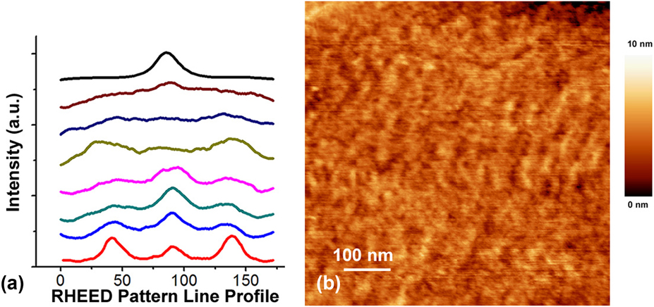
As a comparison, from the RHEED intensity of (Bi0.5Sb0.5)2Te3 films on Nb following the two-step method, the lattice constant of the Bi–Sb–Te passivation layer in the first step [fourth green line in Fig. 4(a)] is smaller than the normal (Bi0.5Sb0.5)2Te3 film in the second step [from fifth pink to bottom red several lines in Fig. 4(a)]. Although the passivation layer is crystalized, it may not be single crystalline. From the RHEED image, the passivation layers are more like textured, not polycrystalline or amorphous. The HRTEM image shows the interface between Nb and (Bi0.5Sb0.5)2Te3 has one QL fuzzy feature at this interface. It means the Bi-Sb-Te passivation layer is only one monolayer thick, and only becomes weakly epitaxial after annealing. We used AFM to make deeper study on this passivation layer, as shown in Fig. 4(b). The rms roughness of this passivation layer is lower than 0.4 nm, nearly the same as the hill top surface roughness. More cycles of the deposition-annealing process in the passivation layer deposition may decrease the roughness of the passivation layer and lead to a smoother (Bi0.5Sb0.5)2Te3 film surface. The passivation layer surface morphology is a smooth and continuous film without pin holes or larger features. The reason why the passivation layer is only weakly epitaxial is that particles in the passivation layer may have a hard time to correctly nucleate at the first layer. Therefore in the first step, we need more growth-annealing cycles to make the passivation layer crystalline and cover properly.
(a) RHEED streak intensity of (Bi0.5Sb0.5)2Te3 thin films on Nb with film thickness. From top to bottom: Nb substrate, passivation layer deposition 0.1 ML, passivation layer deposition nearly 1 ML, passivation layer after annealing, 1 QL deposition, 2 QL deposition, 4 QL deposition, and 15 QL deposition. (b) AFM image of the passivation layer.

The lattice constant of the (Bi0.5Sb0.5)2Te3 film on Nb at the second step is almost the same as (Bi0.5Sb0.5)2Te3 on Si substrates. The lattice relaxation starts mostly in the second step [fifth pink line in Fig. 4(a)], which implies the absence of strain between the passivation layer and the top (Bi0.5Sb0.5)2Te3 layers. The passivation layer effectively blocks the interaction between the (Bi0.5Sb0.5)2Te3 layer and the Nb surface; therefore, only very weak Van der Waals (VdW) interaction remains at the interface. And the other function of the passivation layer is to provide a flat crystalline surface for efficient adatom nucleation and diffusion.
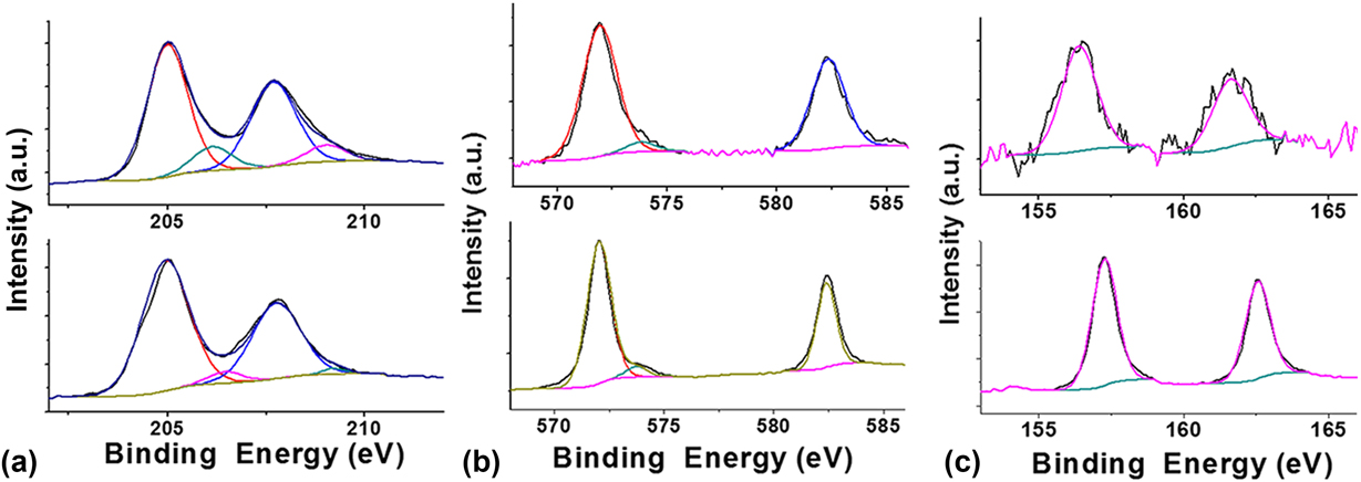
We carried out in situ XPS to characterize the chemical stoichiometry and purity of the passivation layer and the finial (Bi0.5Sb0.5)2Te3 film (Fig. 5). The chemical stoichiometry of Bi/Sb:Te is nearly 2:3 in the passivation layer from the first step and 2:3 in the (Bi0.5Sb0.5)2Te3 film from the second step. Then, we checked the elements’ chemical binding energy shift. The top image of Fig. 5(a) shows the Nb 3d peak before depositing the passivation layer, and the bottom image is Nb 3d after the passivation layer deposition. The top images of Figs. 5(b) and 5(c) are Te 3d and Bi 4f peaks of the passivation layer, and the bottom images are Te 3d and Bi 4f peaks after 6 QL (Bi0.5Sb0.5)2Te3 deposition. The Te 3d peak is fitted using two peaks from Te 3d 5/2 and 3d 3/2, respectively. The Bi 4f peak is fitted with the Bi 4f 7/2 and 4f 5/2 peaks. As the (Bi0.5Sb0.5)2Te3 deposition continues, the Nb 3d peak intensity keeps decreasing while the intensity of the Bi 4f and Te 3d peaks increases. Before and after the passivation layer deposition, the Nb peaks change very little in the line shape and peak position; in addition, the Bi, Sb, and Te peaks in the passivation layer do not change much comparing with the top (Bi0.5Sb0.5)2Te3 layer. These indicate that the negligible chemical reaction occurred between the (Bi0.5Sb0.5)2Te3 layers and the Nb surface because the passivation layer is physically adsorbed and effectively blocks the chemical interaction between the Nb substrate and the (Bi0.5Sb0.5)2Te3 layer.
XPS of the (a) Nb 3d, (b) Te 3d, and (c) Bi 4f core levels of (Bi0.5Sb0.5)2Te3 thin films on Nb following the two-step growth method.

Except for Nb surfaces, we can also apply the two-step method to deposit (Bi0.5Sb0.5)2Te3 on other strong interaction surfaces, such as on the NbN surfaces as shown in Fig. 6. NbN is also a good superconductor with the superconductor transition temperature higher than that of Nb. The RHEED and XRD results show that (Bi0.5Sb0.5)2Te3 is well crystallized on NbN using this two-step growth method. This two-step method also works on epi (0001)-MgB2 and epi (111)-MgO surfaces and achieves single crystal (Bi0.5Sb0.5)2Te3 deposition. To demonstrate that the two-step deposition method applies to more general substrates, we tried to deposit (Bi0.5Sb0.5)2Te3 on Si(111) and SrTiO3(111) surfaces as examples. We readily got perfect (Bi0.5Sb0.5)2Te3 films because the passivation layers more easily form crystalized phase on these surfaces without complications.
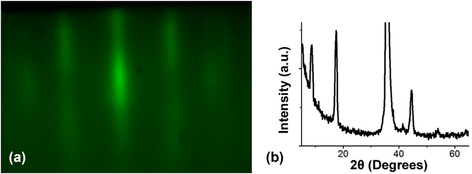
RHEED patterns for (Bi0.5Sb0.5)2Te3 with two-step growth procedures on an NbN surface: (a) epitaxially grown (Bi0.5Sb0.5)2Te3 films after the second step finished. (b) XRD profile of (Bi0.5Sb0.5)2Te3 on NbN.

E. Nb–(Bi0.5Sb0.5)2Te3–Nb heterostructure
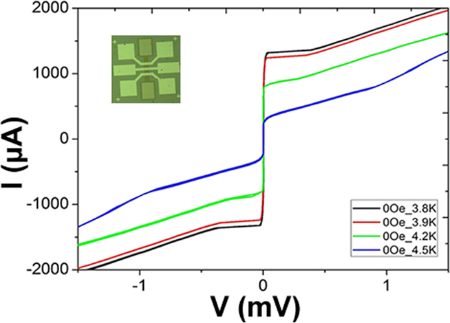
After optimizing the (Bi0.5Sb0.5)2Te3 growth on Nb, we continued to construct Nb/(Bi0.5Sb0.5)2Te3/Nb vertical heterostructures to proximity-couple the TI film on both surfaces. The top Nb layer was prepared by magnetron sputtering at room temperature with same conditions as the bottom Nb layer growth. The superconducting transition temperatures of both Nb layers (50 nm) were measured to be 7.8 K. The fabrication process of the vertical Josephson junctions is similar to the fabrication of epitaxial MgB2 vertical Josephson junctions.Reference Li, Zhang, Yang and Miao39 A picture of the final device is shown in the inset of Fig. 7.
I–V curve of a vertical Josephson junction with 50 nm–Nb/7 nm–(Bi0.5Sb0.5)2Te3/50 nm–Nb and an area of 8 × 16 μm, measured at 3.8 K. The inset is an optical image showing geometry of the device.

Figure 7 shows a typical I–V curve measured from the TI Josephson junction with an area of 8 × 16 μm at different temperatures. (Bi0.5Sb0.5)2Te3 acts as the tunneling barrier and its thickness is about 7 nm. According to the I–V curves, the critical Josephson current at 3.8 K is about 1.8 mA. The I cR N product is about 2.3 mV, comparable to the expected Nb superconducting energy gap. The hysteresis suggests that the junction is underdamped. The good performance of such vertical topological Josephson junctions not only demonstrates the high quality of the deposited (Bi0.5Sb0.5)2Te3 but also paves roads for effectively trapping Majorana fermions within magnetic flux lines. Carefully tailoring the junction geometry can further enable the manipulation of these elusive particles towards quantum information processing.
IV. CONCLUSION
In this article, we used Nb as the superconductor electrode material and deposited epitaxial TI (Bi0.5Sb0.5)2Te3 films on it. We optimized the quality of (Bi0.5Sb0.5)2Te3 thin films grown on Nb by following a two-step MBE deposition method. Bi, Sb, and Te clusters were first deposited at a temperature lower than the normal growth temperature, and the sample was properly annealed to form a compact passivation layer, then we resume the growth of (Bi0.5Sb0.5)2Te3 at the normal growth temperature. The critical growth parameters for the passivation layer and the final film were identified with the help of in situ RHEED as well as ex situ XRD, AFM, XPS, and HRTEM. We found that in one-step depositions, the excess Te and the high temperature favor strong chemical reactions leading to foreign phases and breaking the epitaxy. In the two-step process, the first step at low temperature is dominated by physical absorptions, while the annealing process helps crystallization through solid-state epitaxy without inducing much chemical reactions. Therefore, we are able to obtain clean interfaces and good epitaxy. Finally, Nb/epitaxial (Bi0.5Sb0.5)2Te3/Nb heterostructures were obtained and subsequently patterned into Josephson junctions showing clear Josephson currents, which further confirms the high quality of the materials created with our deposition techniques.
Supplementary Material
To view supplementary material for this article, please visit https://doi.org/10.1557/jmr.2018.195.
ACKNOWLEDGMENTS
This work was supported by Natural Sciences and Engineering Research Council of Canada (NSERC) Discovery Grant Nos. RGPIN-418415 and RGPIN-04178, Ontario Early Researcher Award (ERA), the Canada First Research Excellence Fund, Chinese Academy of Science Pioneer Hundred Talents Program, and the Union funding of National Synchrotron Radiation Laboratory of China. The infrastructure would not be possible without the significant contributions of the Quantum Valley Investments, the Canada Foundation for Innovation, the Ontario Ministry of Research & Innovation, and Industry Canada.