I. INTRODUCTION
Nowadays needs for more multifunctional and compact size systems promote the necessities for small mobile terminals including cell phones, short- and long-range communication devices, handheld portable wireless equipment for internet connection, radio frequency identification, etc. Similarly, small equipment and devices used for data transmission and navigation (GPS systems) necessitate small antennas. Microstrip antennas (MSAs) are very popular in microwave and radio frequency (RF) designs because of their inherent advantages such as low profile, conformability, design simplicity, and low cost [Reference Balanis1].
A number of techniques have been described in the literature to reduce the size of a MSA. One such conventional method of size reduction is incorporation of slots and slits in the patch of a MSA. This reduces the resonant frequency of the antenna, but the performance of antenna suffers [Reference Chen, Wu and Wong2–Reference Chen, Chou and Chiu5]. Some recent developments in the antenna size miniaturization are the inclusion of different fractal geometry and use of different meta-material structures. A dual-reverse-arrow fractal geometry was introduced in a triangular patch antenna in [Reference Orazi and Soleimani6]; as a result a reduction in the antenna size was achieved with a low radiation efficiency and bandwidth. For improving the radiation efficiency an air gap was also introduced with in the structure, but structure became complex and non-planar. A number of antennas inspired by reactive impedance surface (RIS) in combination with slots, complementary split-ring resonators (CSRR), and other meta-material structure have been proposed to design smaller antennas [Reference Kumar and Vishwakarma7–Reference Dong, Toyao and Itoh10]. In [Reference Cai, Wang, Shi and Zhang11], a Hilbert shaped RIS and Wunderlich-shaped fractal CSRR were utilized for size reduction with low substrate thickness. A meta-surface with complimentary pattern was placed on the top of the antenna in [Reference Zhu, Cheung and Yuk12] for miniaturization; in this, the size reduction was achieved on the cost of complexity in the fabrication. The use of meta-materials as a high effective permeability (μ eff > 1) substrate for antenna miniaturization was also reported in [Reference Farzami, Forooraghi and Norooziarab13, Reference Cai, Wang, Zhang, Zong, Wang and Xu14]; designing of these antennas at a particular frequency is very complex due to the drastic change in the material parameters with a small change in the frequency.
A recent emerging technique based on artificially engineered electromagnetic meta-materials is electromagnetic bandgap structure (EBG). These periodic structures were previously proposed at optical regime and were known as a photonic bandgap (PBG) structure or photonic crystal (PC). In [Reference Suntives and Abhari15], a mushroom-type EBG structure operating in the slow wave region was used for microstrip patch antenna miniaturization. The fabrication of this type of antenna having mushroom-type EBG is very complex due to the presence of number of layers and vias. The antenna efficiency of this structure is also low as compared with the conventional antenna. Beside this, the uniplanar compact EBG (UC-EBG) structures are a type of EBG structures which are simple and easy to fabricate since they do not necessitate vias [Reference Yang, Ma, Qian and Itoh16, Reference Chang, Qian and Itoh17]. The use of slow wave region (pass-band) of UC-EBG structures in the antenna design offer size reduction with improved performance, which takes into account of radiation efficiency [Reference Kim, Kim, Yook and Park18–Reference Egels, Deleruyelle, Pannier and Bergere20]. The UC-EBG in pass-band can also effectively reduce the radar cross-section (RCS) of MSA outside operating band. In literature a distorted UC-EBG (DUC-EBG) is utilized for reducing RCS of the microstrip printed dipole antenna [Reference He, Jin and Geng21, Reference Ling, Gong, Lu, Yuan, Wang and Liu22].
In this paper, a miniaturized coaxial feed curved-slotted microstrip patch antenna over a fractalized-UC-EBG (F-UC-EBG) ground plane is proposed at 1.57 GHz GPS band. First, the effect of slots in the patch for antenna miniaturization is carried out, and then the ordinary ground plane is replaced by the F-UC-EBG for further miniaturization with improved performance. The UC-EBG is fractalized to achieve high slow wave factor in the lower frequency region. Here F-UC-EBG is used in the slow wave region for further decreasing the resonant frequency and improving the antenna radiation performance. To the best of authors’ knowledge, the effective use of F-UC-EBG and curved slotted patch in the antenna miniaturization with improved performance was not reported earlier [Reference Chen, Wu and Wong2–Reference Egels, Deleruyelle, Pannier and Bergere20, Reference Liu, Yin and He23–Reference Elsheakh and Abdallah25]. The proposed compact antenna reports a good radiation efficiency of 81.59% even with a small antenna size of 0.184λ 0 × 0.184λ 0 × 0.0236λ 0 at 1.57 GHz GPS band as compared with the antennas reported in the literature [Reference Chen, Wu and Wong2–Reference Suntives and Abhari15], [Reference Kim, Kim, Yook and Park18–Reference Egels, Deleruyelle, Pannier and Bergere20, Reference Liu, Yin and He23, Reference Pflaum, Thuc, Kossiavas and Staraj24]. The proposed miniaturized MSA is a linearly polarized antenna which is designed, fabricated, and tested. The CST Microwave Studio simulation tool is used to design and optimize the antenna structures.
II. CURVED SLOTTED MICROSTRIP PATCH ANTENNA
The microstrip patch antenna acts like a λ/2 microstrip transmission line which operates at its dominant mode and radiates from its two edges [Reference Balanis1]. The resonant frequency of a square patch MSA at its dominant mode can be obtained as
 $${f_r} = {c / 2}\left( {l + h} \right)\sqrt {{{\rm \varepsilon} _e}}, $$
 $${\varepsilon _e} = \left( {{{({{\rm \varepsilon} _r} + 1)} / 2}} \right) + \left( {{{({\varepsilon _r} - 1)} / 2}} \right){\left( {1 + \left( {{{12h} / W}} \right)} \right)^{ - {1 / 2}}},$$
where c is the speed of light, l is the resonant length of the square patch (patch width W = l for square patch), h is the height of the substrate, εe and ε r are the effective and relative electric permittivity of a dielectric substrate respectively. The exact estimation of the resonant frequency relies on the factors, for example, ground plane size and metal thickness.
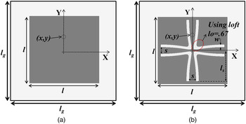
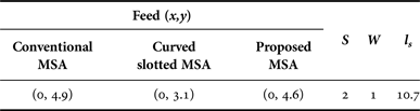
The design procedure of the proposed curved slots loaded microstrip patch antenna over F-UC-EBG ground plane starts with the design of a conventional microstrip patch antenna over an ordinary ground plane that operates at 3 GHz as shown in Fig. 1(a). The conventional antenna consists of a square patch radiator printed on a grounded FR4 substrate (ε r = 4.3, tan δ = 0.025) with thickness of h = 4.5 mm. The dimensions of the square patch and the ground plane are (l × l) = 21.6 × 21.6 mm2 and (l g × l g ) = 35 × 35 mm2, respectively. All the designed antennas are excited by a coaxial feed probe at a point (x, y) with respect to the patch center. The antenna design parameters are given in Table 1. The thickness of copper in all the antenna designs is kept to be 0.017 mm.
Geometry of the antennas: (a) conventional microstrip patch antenna, and (b) curved slotted microstrip patch antenna.

Antenna design parameters (in mm) with loft value l 0 = 0.67.

To reduce the size of the conventional square patch MSA, four curved slots with equal arm length l s , loft value l 0, and narrow slot width w are introduced along the orthogonal direction of the square patch radiator as shown in Fig. 1(b). The two arms of each curved slot are aligned in parallel at a distance s from the center lines of the square patch. By increasing the arm length and loft value of the curved slots, the fundamental resonant frequency of the curved slotted square patch is significantly decreased.
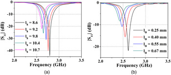
Figure 2 shows |S11| of the curved slotted MSA for different curved slot length l s and loft value l 0. It is observed from Fig. 2(a) that, as the curved slot length l s increases with fixed loft value l 0 = 0.25, the resonant frequency of the curved slotted MSA decreases, this is due to the increment of current path length around the curved slots. Further decrement in the resonant frequency is observed as the curved loft value is increased from 0.25 to 0.67 with fixed l s = 10.7 mm, shown in Fig. 2(b). The optimized value of the curved slot length and the loft is l s = 10.7 mm and l 0 = 0.67, respectively.
Variation of |S11| for the curved slotted MSA over an ordinary ground plane with (a) curve length l s , and (b) curve loft value l 0.

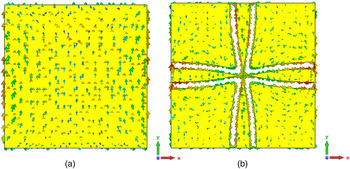
Figure 3 illustrates the current distribution on the surface of the patch at resonance for the conventional microstrip patch antenna and the curved slots loaded microstrip patch antenna. From Fig. 3(a), the current on the conventional square patch flows in a straight path from one radiating edge to another radiating edge. As the curved slots are inserted into the square patch, the current on the patch and the field underneath the patch resonate from one edge of the patch and take the longer path around the curved slots to reach the opposite edge which is apparent from Fig. 3(b). This longer path of the current on the curved slotted patch causes the downshift in the resonant frequency or miniaturization in the physical size of the antenna.
Current distribution on the surface of the patch at resonance: (a) conventional microstrip patch antenna, and (b) curved slots loaded microstrip patch antenna.

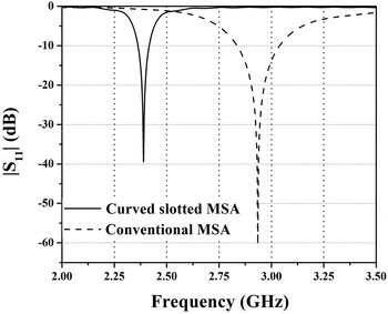
Simulated |S11| for the conventional and curved slotted MSAs are compared in Fig. 4. The simulation results shows, the conventional microstrip patch antenna designed at 3 GHz resonates at 2.93 GHz; this might be due to the finite ground plane size and the metal thickness. It is observed that the curved slotted MSA radiates at 2.38 GHz, a relatively lower frequency as compared with the conventional microstrip patch antenna at 2.93 GHz, which is due to the increment in the current path around the patch radiator. This downshift in the resonant frequency of 18.77% suggests that the curved slotted MSA over an ordinary ground plane is 38.30% miniaturized as compared with the conventional MSA. If a conventional MSA is designed to resonate at 2.38 GHz, the square patch size would be 27.5 × 27.5 mm2. In Section-III and IV, the detailed design process for the F-UC-EBG structure and the proposed antenna are discussed, respectively.
Simulated |S11| for the curved slotted MSA and the conventional MSA.

III. F-UC-EBG GEOMETRY AND DESIGN FOR THE PROPOSED ANTENNA
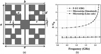
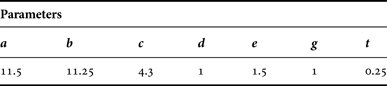
It is difficult to achieve miniaturization and good performance simultaneously, particularly at lower frequencies. The UC-EBG structures have found useful applications in miniaturization and performance enhancement of the MSA. In this article, UC-EBG is fractalized by second order iteration with a scaling ratio of (e/c) = 0.3 and (d/ ((2 × g) + t)) = 0.4 to achieve high slow wave factor in the lower frequency region for miniaturizing the designed curved slot loaded microstrip patch antenna of Section-II. Figure 5(a) shows F-UC-EBG unit cell geometry. The F-UC-EBG unit cell design parameters are given in Table 2. Each unit cell of the F-UC-EBG structure is linked to its four adjacent neighbors through narrow strips. Each of these strips has an inset to increase the inductance per unit length (L) of the microstrip line. Furthermore, the gaps between adjacent lattices produce a coupling capacitance, increasing the capacitance per unit length (C). We can change L and C, thereby controlling the slow-wave effect through the change in the geometry of the strips and the gaps.
(a) Unit cell of the F-UC-EBG structure, and (b) slow-wave factor of F-UC-EBG structure.

F-UC-EBG unit cell dimensions (in mm).

The slow wave effect introduced in the transmission zone of the F-UC-EBG structure below the bandgap region in the relatively lower resonant frequency is utilized for the antenna size reduction. Figure 5(b) shows the slow-wave factor of the 3 × 3 F-UC-EBG array structure on a dielectric (FR4) slab of height 4.5 mm in conjunction with that of conventional microstrip line below. The cut-off frequency of F-UC-EBG structure is around 2.45 GHz that can be controlled by adjusting the unit cell dimensions. It is observed that the slow-wave factor (β/K 0) of F-UC-EBG structure below the cut-off frequency is significantly higher than that of conventional microstrip line even at very low frequencies. This slow-wave effect introduced within the structure is due to the increased inductance and capacitance per unit length. Since the equivalent inductance and capacitance increased, that will decrease the phase velocity on the antenna to minimize the antenna size.
IV. PROPOSED ANTENNA AND EXPERIMENTAL RESULTS
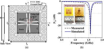
The proposed miniaturized antenna is obtained by replacing the ordinary ground plane of the curved slotted microstrip patch antenna by a F-UC-EBG ground plane, as shown in Fig. 6(a). Due to increased equivalent inductance and capacitance of F-UC-EBG ground plane with in its slow wave transmission zone, the resonant frequency of the curved slotted microstrip patch antenna is downshifted and hence further miniaturization is achieved. The proposed curved slotted MSA over the F-UC-EBG ground plane resonates at 1.57 GHz as shown in Fig. 6(b). The shift in the resonant frequency of the proposed antenna as compared with the conventional MSA at 2.93 GHz is 46.41%. This shift in the resonance of the proposed antenna corresponds to a size reduction of 74.76%. This reduction in the size of proposed patch antenna is calculated with respect to a conventional MSA with a patch size of 43 × 43 mm2 resonates at 1.57 GHz.
(a) Geometry of the proposed curved slotted MSA over F-UC-EBG ground plane, and (b) measured and simulated |S11| of the curved slotted MSA over the F-UC-EBG ground plane. The inset at upper left shows fabricated proposed antenna prototype.

All the antennas are designed with good impedance matching. The proposed antenna is fabricated using Leiterplatten-Kopierfräsen (LPKF) Printed Circuit Board (PCB) prototyping machine. The fabricated proposed antenna is shown in the inset of Fig. 6(b). The measurement of the fabricated proposed antenna is carried out using Agilent vector network analyzer (VNA). The measured and simulated |S11| are shown in Fig. 6(b) and are in good agreement. The resonant frequency of the proposed antenna from measured |S11| is 1.56 GHz. There is a minor difference in the simulated and measured |S11|, which is due to the fabrication tolerances, specially the effect of the effect of stacking the layers of FR4 substrate to achieve the desired thickness of 4.5 mm.
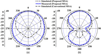
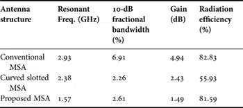
Figure 7 shows measured and simulated radiation patterns in both the principal planes (XZ and YZ) for the proposed MSA at 1.57 GHz. For comparison, a conventional MSA at the same resonance is simulated and its radiation pattern is also plotted in the same plot for both the principle planes. Because resonance is resulting from both the curved slotted patch and the F-UC-EBG ground plane, the proposed antenna is having dipole-like (omnidirectional) patterns with a very low level of cross-polarization unlike the conventional MSA. However, this backside radiation coming from defected ground plane structure does not affect the beam-width at −3 dB. There is a good agreement in the simulated and measured radiation pattern in both the planes. A minor difference in the simulated and measured radiation patterns might be due to the effect of the reflecting environment and the presence of the SubMiniature version A (SMA) connector assembly on the back of the antenna. These omnidirectional characteristics towards the back of the antenna are good for Global Positioning System (GPS) applications at 1.57 GHz band. The simulated gain and radiation efficiency for the proposed antenna are plotted in Fig. 8. It is clearly visible that there is a very small variation in the gain and radiation efficiency of the antenna throughout its operating band. The antenna exhibits an average gain of 1.45 dB over its operating frequencies. At 1.57 GHz GPS band the proposed antenna with 74.76% miniaturization is having a gain and radiation efficiency of 1.49 dB and 81.59%, respectively. The simulated gain, radiation efficiency, and 10-dB fractional bandwidth of all antenna structures are also tabulated in Table 3. In comparison with the conventional MSA, the proposed antenna exhibits a relatively lower gain and bandwidth which is expected as it is electrically small. It is observed that radiation efficiency and 10-dB fractional bandwidth of the proposed antenna is improved with miniaturization as compared with the curved slotted MSA. This enhancement in the antenna performance is due to the better impedance matching at lower frequency by the use of the F-UC-EBG ground plane.
Measured and simulated radiation patterns of the curved slotted MSA over the F-UC-EBG ground plane (proposed MSA) with simulated conventional MSA patterns at 1.57 GHz: (a) XZ Plane, and (b) YZ Plane.

Simulated gain and radiation efficiency of the proposed antenna against frequency.

Comparison of performances of the antennas.

V. CONCLUSION
A curved slotted MSA over the F-UC-EBG ground plane is proposed with compact size and improved performance. The antenna is studied over an ordinary ground plane and the F-UC-EBG ground plane. It can be culminated from the results that the use of curved slots in the patch reduces the antenna size, but the use of the F-UC-EBG structure in the ground plane within its slow wave region improves the antenna radiation efficiency with further reduction in the antenna size. Beside this, the antenna fractional bandwidth is also improved with acceptable gain when the ordinary ground plane of the curved slotted patch antenna is replaced by the F-UC-EBG ground plane. The proposed antenna with good radiation efficiency and omnidirectional characteristics at 1.57 GHz is 74.76% miniaturized and finds appropriateness in GPS applications for portable and handheld communication systems.
 Saurabh Kumar received his B.Tech. degree in Electronics and Communication Engineering from Uttar Pradesh Technical University, Lucknow (India) in 2008 and received his M.Tech. degree in Digital Communication from Guru Gobind Singh Indraprastha University, Delhi (India) in 2010. He is pursuing his Ph.D. degree from Indian Institute of Information Technology, Design and Manufacturing, Jabalpur (India) since 2012. His research interest includes planar and microstrip patch antennas, artificial materials like meta-materials, electromagnetic theory, RF, and microwave engineering, etc.
 Dinesh Kumar Vishwakarma is an Associate Professor of Electronics and Communication Engineering at Indian Institute of Information Technology Design and Manufacturing (IIITDM), Jabalpur India. He received his Ph.D. degree in Electrical Communication Engineering from Indian Institute of Science, Bangalore in 2005. He was a visiting foreign researcher in Japan from 2006 to 2009. Prior to this he was employed in Ministry of Communication & IT through Indian Engineering Services. His research interests include computational electromagnetics, microwave circuits, antenna and wave propagation, photonics and optical communication.