Introduction
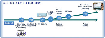
In the past, materials have been developed much earlier than devices that have been applied later. After scientists discovered new materials and defined the basic principles of their synthesis, they found applications in devices that eventually became products. For example, we know that liquid crystals were discovered in 1888,Reference Reinitzer1 but it was about 80 years before RCA produced the first liquid-crystal display (LCD), and Sharp did not introduce the first LCD product until 1975. Thirty years later, in 2005, Samsung commenced mass production of larger sized (82 in.) thin-film transistor (TFT) LCDs (Figure 1).
Materials innovation leading device creation (flat-panel display). The discovery of liquid crystal in 1888 led to the first liquid-crystal display (LCD) 80 years later. Sharp introduced the first LCD product in 1975, with Samsung mass producing larger sized (82”) thin-film transistor (TFT) LCDs in 2005.

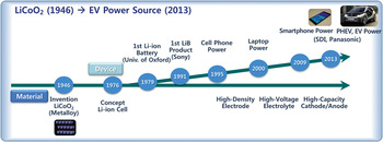
The realization of LCD devices was thus the result of utilizing new functionalities of evolutionary liquid-crystal materials. Lithium batteries followed a similar development. Lithium cobalt oxide was invented by Metalloy in 1946, who filed the first patent on this material. However, the first lithium-ion battery was not developed until 1979 at Oxford University, and another 20 years passed before Sony introduced the first product in the market in 1991.Reference Ellestad and Babbitt2 Since that time, these batteries have evolved as a power source for smartphones, laptops, and even for plug-in hybrid vehicles or for pure electric vehicles (Figure 2).
Materials innovation leading device creation (Li-ion battery). LiCoO2 was first invented in 1946 by Metalloy. It was not until 1979 that University of Oxford researchers developed the first lithium-ion battery, and 20 years later, Sony introduced the first product on the market. These batteries have evolved as a power source for smartphones, laptops, and even for plug-in hybrid vehicles (PHEVs) or for pure electric vehicles (EVs). Note: LiB, lithium-ion battery.

In the past, materials have been discovered before an application was found. At the beginning of the analog era, when cathode ray tubes were introduced, cathodoluminescent materials were already available. However, when the 3G era began in 2000, the evolution of display devices was very fast, and the customers for these devices became demanding; materials were therefore developed to fulfill their requirements. Many highly efficient phosphor materials are available today, but we would like to increase their efficiency; however, we lack deep blue phosphorescent materials. This means that device market requirements are currently somewhat ahead of materials development. In the case of quantum dot (QD) light-emitting diode (LED) materials, we are working very hard to develop highly efficient, low cost, environmentally friendly QD materials, but such devices are already required by the market.
The development of electrolytes has been important for use in batteries. For heavy duty applications or analog devices such as portable devices, aqueous electrolytes (acid or alkaline electrolytes) can be applied such as in lead acid, nickel cadmium, or nickel metal hydride batteries. Since the invention of the lithium-ion battery, they were applied to smartphones, even in electric vehicles, and now we are trying to develop smaller wearable devices. However, development of electrolyte systems, including cathode and anode active materials, still lags behind customer demand for increased energy density, which is directly related to the operating time and driving range of electric vehicles.
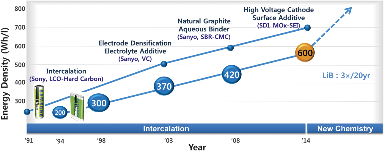
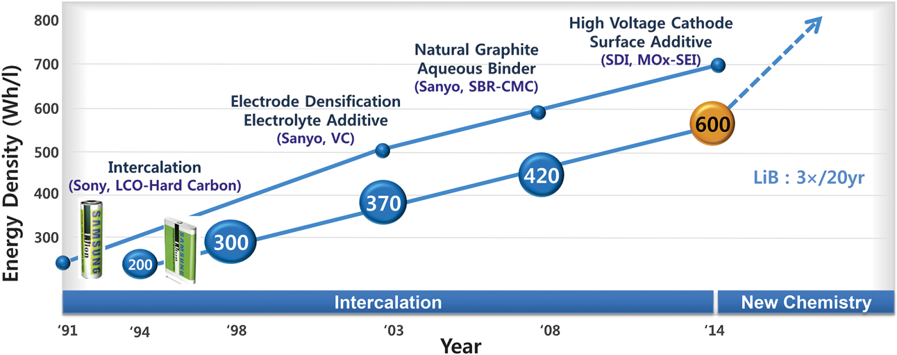
The life cycle of devices is currently much faster than that of materials. Moore’s law states that transistor density doubles and cost is halved every two years. The first lithium-ion battery was marketed in 1991, and the prismatic cell was on the market in 1994, the year I started lithium-ion battery research. At that time, the energy density of the prismatic lithium-ion cell was 200 Wh/l. Over the next decade, researchers and engineers worked hard to improve this. As a result, cathode materials have been changing from lithium cobalt oxide (LCO) to high voltage cathode materials, and hot carbon anode materials have been changing to natural graphite to increase the energy density and also to help the stability of cathode and anode materials. Surface additives have been introduced and electrolyte additives have been developed, but energy density has only been enhanced by a factor of 3 in 20 years (Figure 3). We need a new chemistry for lithium-ion batteries to overcome the low energy density. However, the current market expansion of smartphones is demonstrating a limit to the device revolution.
Device life cycle (Li-ion battery). Developments over the last 20 years have led to a 3× increase in battery energy density. Note: LiB, lithium-ion battery; LCO, lithium cobalt oxide; VC, vinylene carbonate; SBR-CMC, styrene-butadiene rubber/carboxymethylcellulose; MOx, metal oxide; SEI, solid electrolyte interphase.
Prior to 2000, the mobile phone market was worth about $91 billion. Since then, wireless communication has moved from 1G to 4G speed, the long-term evolution (LTE) or LTE-A standard has been utilized, and communication has shifted from voice texts to digital multimedia broadcasting (DMB) using high-speed Internet applications. There has also been a shift from devices with monochromic LCD displays, and full color organic light-emitting diode (OLED) displays are now used in smartphones with touchscreens and curved designs. This revolution has led to an extraordinary market expansion of more than $250 billion in 2010.3 However, in the last two or three years, there has been a marked retardation in the rate3 of growth. How can we achieve another device revolution? The answer may lie in flexible devices or foldable devices with very high energy density batteries and long-lasting battery power. This can only be achieved using novel materials, and this represents a challenge for materials scientists and engineers.
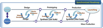
How do we meet the demands of the mobile device user through the application of new materials? In order to do this, materials and devices must be developed simultaneously from the beginning stage of research. We can correlate materials simulation and device simulation at the beginning of the design stage. After that, new materials can be synthesized, and the laboratory scales for these materials can be tested and evaluated by the device developers at the prototyping level. The results can then be fed back to the materials scientists, who can modify the material properties to fit the device applications. Using such a synchronized roadmap, mass production of the materials can be started at the same time as the product launch. Even before launching the product, pretesting at the pilot level can verify that the synthesized materials are suitable for production at the device level (Figure 4).
Accelerating materials and devices research and development via synchronized roadmap.

Display device innovation
Future displays must be flexible, highly efficient, and with high color reproduction. We now have rigid displays in devices, but in the future, they need to be flexible. Consider the market in curved OLED televisions (TVs), which currently have a 4000 mm radius. In order to have a real foldable or flexible device, the curvature should be less than 5R (R is the radius in mm), even less than 1R; eventually they will need to be stretchable. We need the luminescent efficiency to increase from the current 45 cd/A to 70 cd/A. Color reproducibility, on the basis of National Television System Committee (NTSC) numbers, is currently about 75%, and this must be increased to above 130%. For such devices, foldable films, transparent electrodes, phosphorescent materials, and very high contrast luminescent materials are needed.
At present, an ultrahigh definition TV uses approximately 8 megapixels, and this can be increased to 16 megapixels. Mobile applications should be flexible starting from 5R to 1R, and eventually they must be stretchable. In order to have this roadmap for device development, we must start the research and engineering at the same time. LED materials currently achieve around 100 lm/W, and this must increase to more than 250 lm/W to fit to the N + 2 generations of the device, where N is now. OLED materials now have highly efficient red and green emitting materials, but we need deep blue phosphorescent materials both for TV and mobile display device applications.
Perhaps in the future, we may gain some advantage by mixing fluorescent and phosphorescent materials, so-called thermally delayed activated fluorescence materials. To make these mobile display devices flexible and foldable, we need to change every rigid material on the surface in order to have window films and polarizing films with a curvature of 1R or 5R, and also a flexible transparent electrode. For the stretchable devices, we need to have a stretchable TFT and a stretchable electrode.
Battery innovation
Today, battery innovation for electric vehicles and mobile applications is a tradeoff between higher density and safety considerations. Currently, LCO and nanocomposite materials (NCMs) are used for the cathode and graphite for the anode materials. Battery life for mobile applications is typically two to three days or less, but the market requires at least five days. The driving range of an electric vehicle with a regular sized prismatic cell lithium-ion battery is now about 150 km from a single charge, but we need a range of up to 400 km. This is probably the limit of current lithium-ion chemistry, but motorists demand more than 500 km, so we need to change the chemistry to materials such as lithium-sulfur or lithium-air batteries.
In order to meet both device requirements, we need to use different anode and cathode materials. In the meantime, a nanocomposite of the currently available LCO or lithium magnesium oxide (LMO) materials could possibly be used. Silicon could be used as a substitute for graphite. Currently, batteries for electric vehicle applications have an energy density of 130 Wh/kg, but we need to increase this to 400 Wh/kg, which is the limit of lithium-ion battery technology today. The energy density needs to increase to 600 Wh/kg, and in order to have a product to do this, we need to start research on materials such as lithium metal or air catalyst materials. For mobile applications, such as the Galaxy or iPhone 5 and 6, the current energy density is 600 Wh/l. We could increase that to 900 Wh/l by changing some of the chemistry of the anode materials and eventually reach more than 1000 Wh/l.
In order to meet these demands, we need to change the four major battery materials from the cathode, anode, electrolyte, and separators. The cathode and anode materials are very important to enhance the energy density, the electrolyte supports the stability, and the separator supports the safety of the cell. The NCM cathode material supplies about 170 mAh/g, and some of the nanocomposites such as LCO or LMO can increase this up to 250 mAh/g. By introducing sulfur composites or oxygen into the lithium, this can be increased even further. Graphite anodes currently allow about 360 mAh/g, but this can be increased by utilizing silicon and lithium metal. In addition to the high energy density materials for the cathode and anode, we require the materials to be electrochemically stable, so the electrolyte is also very important. We need an electrolyte that is stable at up to 4.5 V and even 5 V. Also, the liquid organic electrolyte needs to be changed to a solid polymer or ceramic to increase the energy density and also improve safety.
Research activities at SAIT
The Samsung Advanced Institute of Technology (SAIT) is the corporate R&D center for the Samsung Group. It has a staff of about 1100 researchers in device systems and materials. In materials research, we are focused on fundamental research in materials for electronic devices. SAIT has a three-tier R&D structure: the first stage is frontier research and new business technology seeding. After we complete development at the laboratory level, we transfer it to the business unit R&D center to provide the next-generation product and technology platform, and finally this is transferred to the development team in the business unit for final production. We have five core technologies in materials science and engineering: organic semiconducting materials, inorganic nanomaterials, optical film materials, battery materials, and metabolic engineering. A few examples from each of these technologies are explained here.
OLED materials have been piloted at the device level. The research target for these OLED materials for mobile applications is 70 cd/A, with a T95 (the time at which efficiency has decreased by 5% from its initial value) of 300 hours. Red phosphorescent materials have been available since 2011, and last year, we made our first green phosphorescent materials. Now we are working hard to develop deep blue materials, so if we combine these, we can increase the efficiency by a factor of three. For example, last year the performance of the green host was about 70 cd/A, and now we are approaching 130 cd/A. By combining with the common layers of hold transport layer and electron transport layer structures, we have increased the T95 lifetime (lifetime at 95% efficiency) from 120 hours to about 300 hours, and we expect to eventually reach 400 hours.Reference Hudson, Wang, Helander, Lu and Wang4,Reference Kim5
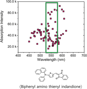
Another application of the organic semiconducting materials group is for organic photodiode (OPD) materials. One example is a complementary metal oxide semiconductor (CMOS) image sensor; by increasing the resolution from 16 megapixels up to 24 megapixels using silicon materials, we found a steady decrease in contrast. By placing the green organic absorbing materials on top of the silicon material, we can obtain adequate sensitivity even at high resolution. To achieve this, we first performed simulations to find the right green organic absorbing material, which had a high absorption sensitivity at a wavelength of 550 nm. Organic photodiode materials on silicon image sensors can provide a high sensitivity compared with pure inorganic materials. This resulted in a patent for application to image sensors in organic CMOS systems (Figure 5).Reference Ro6
Green absorbing materials simulation targeting 16 MP complementary metal oxide semiconductor image sensor. Simulations show that high absorption sensitivity is obtained at a wavelength of 550 nm (green box).Reference Ro6

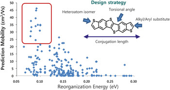
In another application, organic thin-film transistors, we tried to increase the mobility in flexible transistors to above 50 cm2/Vs.Reference Park7 By simulating new designs of molecules such as acene or heteroacene, we have exceeded the mobility of silicon. By controlling heteroatom isomers and alky/aryl substitution and changing the torsional angles and the conjugation length, we discovered many different types of new materials. Some of these materials have already been synthesized, with mobility above 15 cm2/Vs, and now we are synthesizing materials with potential mobility above 30 cm2/Vs. This means that in the future, organic transistors can be used to make flexible and stretchable device circuits (Figure 6).Reference Park7
Novel organic molecules design targeting a 50 cm2/Vs flexible transistor. Many different types of new materials were discovered by controlling heteroatom isomers and alkyl/aryl substitution and changing the torsional angles and conjugation length (upper right schematic). Some of these synthesized materials have mobilities higher than 15 cm2/Vs (red box).Reference Park7

We have an active research program at Samsung in inorganic materials, and the example I have chosen is from the area of high-efficiency thermoelectric materials. Our target is to have a coefficient of performance (COP, ratio of the energy transferred to the electric energy used) greater than 3.5 for a cooling device using thermoelectric materials. We started to design low thermal conductivity materials by applying grain-boundary engineering to maximize the dislocations on the largest surface area of the grain boundary, and we obtained a COP of more than 2.5 for a ΔT (T, temperature) of about 10 K, with a zT max, the thermoelectric dimensionless figure of merit, of about 1.8.
Next, we considered films for foldable applications. Utilizing OLED materials combined with foldable films, we can construct a device that can be folded once or twofold, and inward and outward, that will provide another innovation in mobile devices. In order to do this, hard and foldable films are needed. Polyimide materials can serve this purpose when fabricated in the following process. First, the solvent casting method is used to produce a soft 50 μm film of polyimide. Then, hard coating materials are added. The result is equivalent to about 8H pencil hardness, which is 1H lower than regular glass materials, and transmittance is almost 90% at the moment.Reference Kim, Won and Jung8,Reference Cho, Androsov, Ko and Mikhail9 The polyimide monomers must be designed to minimize the charge transfer complex of the polymer chains.
In addition to these window films, we also require anti-reflecting foldable polarizable films. Currently available polarizable films for rigid applications are based on polyvinyl acetate films, sandwiched between cellulose triacetate films, but this has a thickness of about 90 μm,10 which is impossible to fold into 5R and 1R. We are now developing ultrathin polarizer films by using polypropylene materials embedded with dichroic dye materials as a single layer.Reference Lee, Moon, Won, Kim and Jung11 A new material should be designed for the dichroic dye material by utilizing molecular structures of the rigid-rod aromatic dyes, which can easily be oriented toward the stretching direction when the films are processed. The materials under testing have a color shift of blackness (number of black pixels) less than 3.5, and folding to 3R is available.
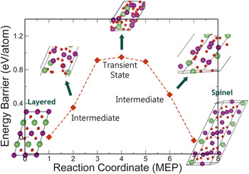
In terms of battery research, the target for electric vehicles is 400 km for a single charge. We need to select the highest cathode capacity material. Inside the chemistry of the lithium-ion battery, a nanocomposite of the overlithiated layered oxide has the highest energy density currently obtainable, about 250 mAh/g. However, we still do not fully understand the degradation mechanism of this material, so we are working to discover how this material degrades and to understand the voltage drop during the charging and discharging by the cycling. We performed composition design using density functional theory (DFT) calculations to suppress the phase change during the charging and discharging and found that with a high energy barrier, we can maintain the layer of the structures from the end of the cycling. We are currently conducting an in-depth study of over-lithiated oxide materials (Figure 7).Reference Mun, Park, Yoon, Park, Choi, Kang, Kim and Doo12,Reference Kong, Longo, Park, Yoon, Yeon, Park, Wang, Santosh, Doo and Cho13
Density functional theory simulation for high capacity cathode materials targeting 400-km electric vehicle driving with single charge. By suppressing the phase change during charging and discharging and if a high energy barrier is used, the layer of the structures from the end of cycling can be maintained.Reference Mun, Park, Yoon, Park, Choi, Kang, Kim and Doo12,Reference Kong, Longo, Park, Yoon, Yeon, Park, Wang, Santosh, Doo and Cho13 Note: MEP, minimum energy path.

Many different types of silicon anode structures and synthesis methodologies are discussed in the literature and developed by companies. This is a very challenging area of research. One approach is to utilize a silicon core covered with a carbon shell to form a nanofiber for enhancing the cycle life.Reference Lee, Yang, Jung and Yu14 We have developed a material with a silicon core covered with a polyacrylonitrile shell, and we can maintain the silicon buffers inside covered with a carbon shell. This is at a very early stage of material development, and now has the capacity density of 1100 mAh/g with about three times longer cycle life than the bare silicon materials. However, this is not the final solution. There are many different methodologies to be realized using silicon anode materials.
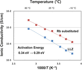
The electrolyte is very important for high energy density batteries, with the aim of changing the anode from graphite or silicon to lithium metal. In order to use lithium metal as an anode, we need to control dendrite formation during the alloying and de-alloying of the lithium metal. The electrolyte is required to have very good mechanical properties, maintaining the same ionic conductivity as the organic electrolyte. This type of design of the block copolymers, combined with an ionic liquid, will increase the mechanical strength of the solid polymer electrolyte while maintaining almost the same ionic conductivity.Reference Lee, Yang, Choi and Lee15 For batteries to be 100% safe in the future, we need ceramic electrolytes. Sulfide systems or oxide systems are available, and there is considerable research in this area. For processability and also stability of the chemicals, we focus on oxide-based garnet structures. If we use rubidium-substituted garnet structures, we can get about 10–3 Siemens/cm at ambient temperature. This type of polymer electrolyte for lithium metal batteries and ceramic electrolyte for all-solid batteries will enhance the energy density as well as the safety of batteries in the future (Figure 8).Reference Park, Lee, Kim, Baek, Ito and Aihara16
Plot of ionic conductivity versus temperature for electrolytes. Ceramic electrolyte (Rb-substituted garnet structure, red data) targets 1.5× longer life than LLZ (blue data) and is the ultimate safe solid-state battery. Note: T, temperature; LLZ, Li7La3Zr2O12.Reference Park, Lee, Kim, Baek, Ito and Aihara16

Calculation methodology and materials informatics
We started our research into all the applications, described previously, with a synchronized roadmap of the device and materials. For faster progress in the laboratory as well as accurate testing, we developed a number of methodologies.
In the very early stage, tacit knowledge was the basis of experiments. From the 1980s up to 2000, the US Department of Energy (DOE) experimental methodology was used, and the Teoriya Resheniya Izobretatelskikh Zadatch (TRIZ) theory of inventive problem solving was also found to be a very useful tool for the design of experiments. Following the DOE, we use factorial design, the Taguchi method, and optimization methodology. We have been able to make a number of breakthroughs using these TRIZ and DOE methodologies, but it is still very time consuming. Enhancement of computing power has enabled us to perform many simulations and modeling of materials for high throughput screening.
High throughput screening methodology, connected with advanced analytical science, can produce so-called materials informatics. Materials informatics in our center is at an early stage of development, but high throughput screening is proving successful. When we first started computations of organic semiconducting materials, we included two fragments, A and B, in the design tool, then calculated the energy levels (highest occupied molecular orbital or lowest unoccupied molecular orbital levels), which required three hours of computing time; calculation of the absorption intensity and absorption peak to calculate the absorption level required another five hours; then calculation of the reorganization energy took more than a day. We then discovered another methodology: Auto Designer. If we take the same A and B fragments, we can perform the same calculations in eight hours—a decrease in the simulation time from 1.5 days to 0.3 days for one material. This means that we can perform an increased number of simulations and produce a larger quantity of material data in a shorter time period.
Another example for battery materials is a high throughput calculation for the redox potential of organic materials using automated DFT calculations and data interpretation for electrolyte materials. We found many types of organic materials, with 5- and 6-membered rings and foreign elements. Based on this materials screening, we can map out these data for the redox potential. We now have about 140 compounds that have been screened. We can thus utilize this information for film formation of cathode materials with oxidation potential less than 4 V.Reference Park, Kang, Im, Doo and Chang17
Using materials informatics, we can also study genomes and proteins to apply to biomolecules; there is existing chem-informatics to study chemicals in the form of small molecules for drug applications. Materials scientists would like to start studying chemicals in the bulk state to apply to organic and inorganic materials.
This methodology can also be applied to OPD design. We can calculate some materials properties for organic CMOS imaging sensor (OCIS) materials, and then calculate the forward chaining, so-called quantitative materials-to-product relationship (QMPR). If we have sufficient data, we can go backward from the device properties and select the materials molecular properties, so-called QPMR. Our dream is to perform such materials informatics on every material, but we are only at the beginning stage of understanding the molecular blend matrix in terms of OCIS materials.
Quantum mechanics simulations can be used to obtain the full width at half maximum of materials. By utilizing such informatics, we can select some known materials and then use the results of the simulation to compare with published data; the accuracy is better than 90% on average. We can then simulate unknown materials; we have been able to obtain 85–90% accuracy with this method. If this material is included in an actual synthesis, we have proved that the accuracy is about 75%.
The advanced methodology of the experiment must be correlated with the analytical science result. We perform two different methods of analysis: one is a combinative analysis, in which we find properties of the materials using experiments in situ and ex situ. For example, for the overlithiated oxide cathode, we analyzed structural deformation to study the phase of the oxidative state and atomic level changes during charging and discharging of the cathode materials. By utilizing in situ x-ray diffraction, in situ x-ray absorption near edge structures, and also ex situ transmission electron microscopy correlated with the simulation data, we found that degradation of the nanocomposite of the overlithiated oxide mostly occurs in the LMO phase at the beginning stages of the cycle life. This gave us a clue to find dopant materials that can suppress these reactions.
Another methodology is complementary analysis. To observe and analyze one spot in a specific area, we have developed many kinds of analysis methodologies at the same position of the specimen using scanning electron microscopy, atomic force microscopy, Raman mapping, and infrared imaging at the same location at the interface of a silicon anode material. We found that the solid electrolyte interphase (SEI) is not uniformly distributed but is localized, and this helped us to find electrolyte additive materials for SEI formation in a uniform area of the silicon anode material.
Summary
I have described some examples of the methodology of experiments performed using a synchronized device and materials roadmap. If we move from creation of new materials to the massive global marketplace by utilizing this kind of methodology, materials functionality can be added to materials, and these materials can be used in innovative novel devices.
If we can evolve new innovations in this way, we can increase the market value for display devices and the semiconductor and battery devices market to more than $550 billion by 2018.18 The display materials market is currently more than $100 billion, and the battery market is more than $10–20 billion. Hopefully, with roadmap alignment and advanced methodologies described, we can accelerate materials innovation for new functionalities in devices.

Hyuk Chang is Director of the Materials Research Center at Samsung Advanced Institute of Technology (SAIT), a corporate research center of Samsung Electronics, South Korea. He holds a PhD degree in metallurgical engineering from the University of Utah (1990) and worked in the Materials Science and Engineering Department at the University of Illinois at Urbana-Champaign as a research associate prior to joining Samsung in 1992. In 2011, he was appointed Samsung Fellow, the highest honor given to Samsung’s researchers and engineers, in recognition of his technological leadership. He has been working on electrochemical energy conversion and storage materials research, and has developed functional materials for fuel cells and rechargeable batteries for application to mobile devices and electric vehicles. He has over 120 technical publications and holds 30 US patents. Chang can be reached by email at hyuk.chang@samsung.com.