Introduction
Strain is a key parameter controlling various physical phenomena coupled to the electronic band structure and defect distribution in materials. Local strains can be used to modify material properties as well as mechanical strength or the lifetime of the material.Reference Li, Shan and Ma1 Measuring and controlling the strain at the nanoscale is fundamental for tailoring both functional and mechanical properties. Elastic strain engineering is widely used in the semiconductor industry to improve the performance of modern devices.Reference Chidambaram, Bowen, Chakravarthi, Machala and Wise2 Strain fields are getting increasingly complex, showing nanoscale nonuniform distributions, requiring measurement techniques with high spatial resolutions. Similarly, local stresses around individual defects and their behavior during deformation are the fundamental factors determining the mechanical response of a material, requiring knowledge of the local elastic strain over time.Reference Hirth and Lothe3
Elastic strain is fundamentally the displacement of individual atoms from their relaxed position, and its components are directly linked to the stress components via the elasticity constants.Reference Nye4 These stresses and strains are not easy to determine, as variances in chemical composition influence the atomic distances, and manufacturing processes induce locally varying residual stresses. A quantitative stress and strain measurement therefore often requires certain assumptions (such as a stable local composition), and only allows for relative measurements. The local elastic strain can only be evaluated with respect to a reference region, which is assumed to be relaxed. This allows for the measurement of relative local changes in lattice parameters. Furthermore, if the investigated material is being deformed, a distinction has to be made between elastic strain related to local distortions of the lattice and plastic strain. The local elastic strains occurring during deformation are directly related to the local stresses; it is important to note that they are transient and thus have to be measured in situ during loading of the specimens.Reference Gammer, Kacher, Czarnik, Warren, Ciston and Minor5
A wide range of strain mapping techniques have been developed, which can be divided into imaging techniques and diffraction techniques. The local plastic strain can be determined by digital image correlation (DIC). This technique tracks multiple features to map the local plastic distortion in the sample.Reference Quinta da Fonseca and Di Gioacchino6 Using transmission electron microscopy (TEM), atomic resolution can be achieved by imaging atomic columns, which directly determines the local elastic strain from the lattice distortions.Reference Hÿtch, Putaux and Penisson7,Reference Hÿtch and Minor8 Most frequently, however, diffraction techniques are used to measure the local elastic strain, using the Bragg relation that directly links the positions of diffraction peaks to the lattice parameters. This includes the use of x-ray diffraction (XRD),Reference Li, Shan and Ma1 neutron diffraction,Reference Krawitz and Holden9 and electron diffraction.Reference Hÿtch and Minor8
Complex strain distributions require that the local strain is measured with high spatial resolution across the full field of view. Because samples have a given thickness and a two-dimensional (2D) signal typically results from a three-dimensional (3D) sample, there is a projection problem. The resolution of a method must be assessed in terms of a volume giving rise to a single strain value. In addition, for most approaches, only the 2D strain tensor is accessible and the specimen needs to be carefully oriented. These problems can be overcome with tomography approaches.Reference Sedmák, Pilch, Heller, Kopeček, Wright, Sedlák, Frost and Šittner10
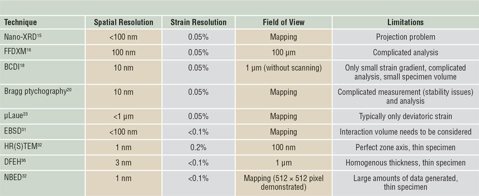
When comparing different strain-mapping techniques, spatial resolution, maximum field of view, and achievable strain resolution are the most crucial parameters. Table I overviews the typical parameters and the main limitations for the different methods. While there has been success in improving the spatial resolution for all methods, it is important to relate the desired length scale with the grain size of the investigated materials. If the resolution is significantly smaller than the grain size, the local strain distributions throughout an individual grain are mapped. On the other hand, if the resolution is significantly larger than the grain size, the Debye–Scherrer diffraction pattern, resulting from a large number of grains, can be used for strain mapping.Reference Zeilinger, Todt, Krywka, Müller, Ecker, Sartory, Meindlhumer, Stefenelli, Daniel, Mitterer and Keckes11
Summary of the most important techniques for elastic strain mapping.

Nano x-ray diffraction (XRD), full-field diffraction x-ray microscopy (FFDXM), Bragg coherent diffraction imaging (BCDI), Bragg ptychography, Laue microdiffraction (µLaue), electron backscatter diffraction (EBSD), high-resolution (scanning) transmission electron microscopy (HR[S]TEM), dark-field electron holography (DFEH), and nanobeam electron diffraction (NBED).The main limitations and typical parameters are compared for all methods.
Strain mapping using XRD
XRD is a vital tool for measuring spacing between atomic planes, and the diffraction process is best visualized by the intersection of a sphere with a radius depending on the wavelength—the Ewald sphere—with the reciprocal lattice. In the case of Laue diffraction, a polychromatic beam is used and a large number of diffraction peaks are accessible.Reference Li, Shan and Ma1 On the other hand, if monochromatic x-rays are used, the sample has to be correctly oriented to measure the desired Bragg reflections. The strain in the measurement frame depends on both the geometry and the strain tensor, with respect to the sample reference frame. Thus, the full strain tensor can be obtained by measuring multiple different reflections.
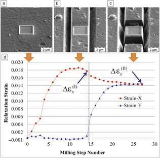
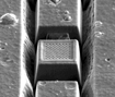
Often, residual stress in a material is of interest and strain is converted to stress using the elasticity constants. If a principal stress direction is known, assumptions can be made to reduce the required number of strain measurements. Most prominent is the measurement of the residual stress in a thin film.Reference Noyan and Cohen12 A different approach to measure residual stresses is based on incremental focused ion-beam milling. Upon material removal, stress redistribution results in material relaxation, and different geometries have been proposed to measure this stress.Reference Noyan and Cohen12,Reference Treml, Kozic, Zechner, Maeder, Sartory, Gänser, Schöngrundner, Michler, Brunner and Kiener13 Figure 1 shows the use of four-slot milling for residual stress analysis of a CrN thin film on a micron scale.Reference Sebastiani, Eberl, Bemporad, Korsunsky, Nix and Carassiti14
Residual stress evaluation via four-slot focused ion beam milling of a CrN coating. (a) A Pt pad serves as a reference surface for digital image correlation (DIC). (b) In step I, a two-slot milling sequence is performed for uniaxial stress relief followed by (c) a second milling sequence in step II for full biaxial stress. (d) Using DIC, the relaxation strain as a function of milling step can be calculated and used to determine the average residual stress in the coating at the micron level. The x direction is normal to the extent of the first slots and the y-direction parallel to the first slots. Strain-X is strain in the x direction, Strain-Y is strain in the y direction.Reference Sebastiani, Eberl, Bemporad, Korsunsky, Nix and Carassiti14

While traditionally XRD yields one global value, recently, the use of finely focused synchrotron radiation has enabled scanning over a specimen, allowing local elastic stress and strain to be determined locally.Reference Cornelius, Davydok, Jacques, Grifone, Schülli, Richard, Beutier, Verdier, Metzger, Pietsch and Thomas15 Nowadays, x-ray beam diameters below 100 nm can be reached at various beamlines. Recent instrumentation allows for fast scanning x-ray microscopy, where a 2D map is recorded containing a full reciprocal space pattern for each position of the sample. If the energy of the incident x-ray beam is varied, even the 3D distribution in reciprocal space can be recorded, without needing to tilt the specimen.Reference Cornelius, Davydok, Jacques, Grifone, Schülli, Richard, Beutier, Verdier, Metzger, Pietsch and Thomas15
An alternative approach to obtain the entire information comprising real and reciprocal space is full-field diffraction x-ray microscopy (FFDXM). To draw an analogy to TEM, the two approaches would correspond to scanning diffraction and dark-field imaging. The advantage of FFDXM over scanning XRD lies in the large field of view and its relatively short acquisition time of few seconds.Reference Simons, King, Ludwig, Detlefs, Pantleon, Schmidt, Snigireva, Snigirev, Poulsen, Stöhr, Snigireva, Snigirev and Poulsen16 A second rather new development is the use of Bragg coherent diffraction imaging (BCDI). In the diffraction signal, the phase is lost and it is not possible to obtain the real-space object directly, but this can be overcome using complex phase-retrieval algorithms. Continuous progress in instrumentation and computation has allowed strain mapping with a spatial resolution below 10 nm. The technique even permits 3D imaging of strain in single nanocrystals and determination of the full strain tensor by measuring multiple reflections.Reference Hofmann, Tarleton, Harder, Phillips, Ma, Clark, Robinson, Abbey, Liu and Beck17,Reference Newton, Leake, Harder and Robinson18
While BCDI is a promising technique, its use for strain mapping of materials containing many defects or large strain gradients remains challenging.Reference Pfeifer, Williams, Vartanyants, Harder and Robinson19 Another possibility is Bragg ptychography, a scanning BCDI technique, which exploits data redundancy to recover information about the sample and illumination. It is more robust and allows 3D imaging of strain, defects, and crystalline plane rotations in extended samples.Reference Takahashi, Suzuki, Furutaku, Yamauchi, Kohmura and Ishikawa20,Reference Godard, Carbone, Allain, Mastropietro, Chen, Capello, Diaz, Metzger, Stangl and Chamard21
Finally, Laue diffraction can be used to measure elastic strain.Reference Zhang, Castelnau, Bornert, Petit, Marijon and Plancher22 The dilatational component of the strain tensor can only be measured if the reflection energy positions are also measured. The strong point of Laue diffraction lies in the possibility of measuring very small lattice rotations by following the movement of diffraction spots on the detector, allowing to track deformation gradients throughout the experiment. Careful analysis of the shape and position of Laue spots allows resolution of crystal defects. Measuring the accumulation of defects such as dislocations provides information on defect structure evolution and correlation to local plastic strain. With the development of Laue microdiffraction mapping, it is possible to scan a sample with submicrometer resolution.Reference Kirchlechner, Keckes, Motz, Grosinger, Kapp, Micha, Ulrich and Dehm23
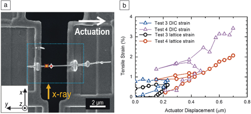
The increased brightness and coherence of modern synchrotron sources in conjunction with faster detectors has opened up the possibility of combining XRD with in situ deformation.Reference Cornelius and Thomas24 Laue microdiffraction determines lattice orientation, deviatoric strain tensor, and local rotations, and is compatible with various mechanical testing geometries, including compression and bending. Similarly, Bragg coherent diffraction can be combined with in situ deformation. Figure 2 shows a recent example demonstrating strain mapping in an individual Au nanowire during deformation using Bragg coherent diffraction.Reference Shin, Cornelius, Labat, Lauraux, Richard, Richter, Blanchard, Gianola and Thomas25 Finally, x-ray nanodiffraction can be combined with in situ deformation techniques to map strain during loading.Reference Zeilinger, Todt, Krywka, Müller, Ecker, Sartory, Meindlhumer, Stefenelli, Daniel, Mitterer and Keckes11
Bragg coherent diffraction imaging during in situ deformation. (a) An individual Au nanowire is mounted on a microelectromechanical systems-based tensile stage. (b) During the tensile tests, lattice strain from Bragg peak analysis was measured and compared to the plastic strain obtained using digital image correlation (DIC). The differences in elastic strain between tests 3 and 4 are caused by slightly different scan areas.Reference Shin, Cornelius, Labat, Lauraux, Richard, Richter, Blanchard, Gianola and Thomas25

Strain mapping in the scanning electron microscope
The scanning electron microscope (SEM) is a versatile instrument offering a variety of analysis techniques, such as the ability to map chemical distributions, image surface topographies and dislocation structures, or to determine local crystallographic orientations using electron backscatter diffraction (EBSD). The latter involves the acquisition of Kikuchi diffraction patterns from each probe position during scanning and using the Kikuchi bands to obtain the local orientation. More recent developments involve the acquisition of high-resolution patterns and analyzing small relative deformations among various patterns. This yields the deformation tensor, including out-of-plane strains, independent of the crystal orientation.Reference Wilkinson, Britton, Jiang and Karamched26 This so-called Wilkinson method is a new technique that has been applied successfully to various materials systems.
While the spatial resolution of EBSD is good, care has to be taken that the signal is not merely from the surface, but results from the electron beam interacting with the sample volume. In addition, obtaining high-quality Kikuchi patterns can be challenging in the case of highly strained specimens. Recently, the use of transmission Kikuchi diffraction, relying on the use of a thin sample and collecting the pattern in transmission, has allowed a significant increase in spatial resolution.Reference Yu, Liu, Karamched, Wilkinson and Hofmann27,Reference Sneddon, Trimby and Cairney28
In situ deformation in the SEM has become increasingly common through the development of a wide variety of compatible testing platforms, including nanoindenters and tensile stages.Reference Dehm, Jaya, Raghavan and Kirchlechner29 Deformation localization observed through surface steps provides a great deal of information on deformation mechanisms. To quantify local plastic strain, DIC can be used; recent developments involving the use of small markers enable DIC at a subgrain level.Reference Quinta da Fonseca and Di Gioacchino6,Reference Stinville, Vanderesse, Bridier, Bocher and Pollock30 Of special interest is the local elastic strain at an individual grain level. Recent work has demonstrated the exciting possibility of combining EBSD strain mapping with in situ deformation testing.Reference McLean and Osborn31
Strain mapping in the TEM
TEMs are particularly powerful tools for strain mapping, due to the ability to spatially resolve strain at the nanoscale with high precision.Reference Ozdol, Gammer, Jin, Ercius, Ophus, Ciston and Minor32 In addition, modern TEMs offer a wide range of techniques, ranging from analytical methods to diffraction and imaging. One obvious drawback is that TEMs require the use of rather thin specimens. This can induce strain-relaxation effects.Reference Jacob, Androussi, Benabbas, François and Lefebvre33
The highest resolution can be obtained from very thin samples, and if the crystal is oriented along the zone-axis, atomic-resolution TEM allows imaging of the lattice structure. High-resolution TEM (HRTEM) is frequently used to image the projected lattice, but care has to be taken as the contrast also depends on other parameters such as sample thickness, defocus, and lens aberrations.
High-angle annular dark-field (HAADF) scanning TEM (STEM) can be used as an alternative. In this mode, the contrast in the image directly represents the positions of the atomic columns. Drift and scanning artefacts strongly influence the strain analysis, but recently, the use of data processing has been shown to reduce this problem.Reference Ophus, Ciston and Nelson34 Imaging the lattice requires the specimen to be on an exact zone axis throughout the entire field to reduce it to a diameter of several hundred nanometers.
Traditionally, the local strain is measured in Fourier space using geometric phase analysis (GPA).Reference Ozdol, Gammer, Jin, Ercius, Ophus, Ciston and Minor32 This involves a filter centered on a Bragg spot in the Fourier transform and calculating the inverse Fourier transform. While the displacement can only be measured in the direction of the chosen reciprocal lattice vector, the use of multiple spots allows computation of the 2D deformation tensor. On the other hand, the strain can be computed from the atomic-resolution images by directly locating the positions of the atoms, which are frequently used in combination with HRSTEM.Reference Mahalingam, Haugan, Brown and Eyink35 Furthermore, dark-field electron holography (DFEH) is a recent technique that is based on directly measuring the phase of the diffracted beams. DFEH is routinely used in the semiconductor industry owing to its precision and ability to map rather large fields of view, but it requires a dedicated microscope equipped with an electrostatic bi-prism. Alternatively, in-line DFEH is based on the use of focus series reconstruction.Reference Houdellier, Hu, Snoeck and Hy36,Reference Koch, Özdöl and Van Aken37 In addition to the geometric phase related to the local distortion, there are other contributions such as electrical and magnetic fields in the specimen, the specimen thickness and other dynamical effects, requiring a sample with homogenous thickness and uniform orientation, which causes the main limitation to the technique.
Nanobeam electron diffraction (NBED) is a promising method in overcoming these limitations and is becoming increasingly popular. NBED uses the positions of the Bragg spots in a zone-axis diffraction pattern. A benefit of electron diffraction is the strong interaction of electrons with matter that makes it possible to obtain diffraction patterns from small sample volumes. Traditionally, a parallel electron beam is used, yielding diffraction with sharp Bragg peaks but limited resolution in real space, typically on the order of 3 nm. The use of a more converged electron beam allows for subnanometer resolution strain mapping. The beam size and thus spatial resolution of the technique is dictated by the maximum convergence angle that can be used without overlap between the disc-shaped Bragg spots. The resulting diffraction pattern yields isolated diffraction discs; modern disc recognition algorithms determine their positions with subpixel accuracy.Reference Pekin, Gammer, Ciston, Minor and Ophus38,Reference Mahr, Müller-Caspary, Grieb, Schowalter, Mehrtens, Krause, Zillmann and Rosenauer39
For strain mapping, the electron beam is scanned across the region of interest and for every probe position, a full diffraction pattern is acquired. The diffraction pattern requires sufficient resolution to track small shifts in the Bragg peaks, thus yielding large amounts of data—easily several hundred gigabytes. NBED has previously been limited by the speed of conventional CCD cameras. Recently, the use of direct electron detectors in combination with efficient evaluation algorithms has enabled strain mapping of areas with high spatial resolution.Reference Ozdol, Gammer, Jin, Ercius, Ophus, Ciston and Minor32 Difficulties for thick specimens stemming from dynamical and inelastic scattering effects can be overcome through zero-loss energy filteringReference Hähnel, Reiche, Moutanabbir, Blumtritt, Geisler, Höntschel and Engelmann40 and precession electron diffraction (PED).Reference Wang, Rouviere, Murray, Bernier and Bruley41 While PED can be used with many conventional TEM instruments, the precessing tilted incident electron beam increases the obtained spot size.
The techniques previously discussed develop their full potential when combined with in situ testing techniques. In situ testing in the TEM has made enormous progress, and modern in situ deformation specimen holders allow for high-resolution measurements of load and displacement. In addition, the local plastic strain can be acquired using DIC, which can provide additional insights if deformation localization occurs.Reference Chisholm, Bei, Lowry, Oh, Syed Asif, Warren, Shan, George and Minor42
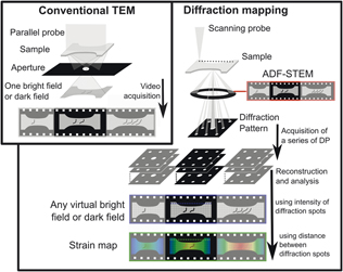
Still, fundamentally, deformation is controlled by defects, and their behavior is defined by local stresses rather than a global stress. Uncovering their physical nature requires true nanoscale strain mapping. While HRTEM imaging provides the required resolution for mapping the strain field around dislocations, local mistilts of the TEM specimen due to bending are inevitable during deformation, hindering atomic-resolution imaging. Ultrathin samples are the exception, allowing HRTEM imaging, even during in situ deformation.Reference Zheng, Cao, Weinberger, Huang, Du, Wang, Ma, Xia and Mao43,Reference Wang, Liu, Guan, Yang, Sun, Cheng, Hirata, Zhang, Evan, Chen and Han44 NBED, on the other hand, offers the required robustness that is necessary to apply strain mapping to standard deformation geometries. Figure 3 shows the experimental setup for NBED, where mapping is carried out during in situ deformation allowing local time-resolved strain maps to be obtained.Reference Gammer, Kacher, Czarnik, Warren, Ciston and Minor5
Experimental procedure of the in situ nanobeam electron diffraction (NBED) technique. In a conventional deformation experiment in the transmission electron microscope (TEM), a sample is deformed, and a video is acquired using a chosen imaging condition. During NBED mapping, a video is acquired in using the annular dark-field (ADF) detector in scanning transmission electron microscopy (STEM) mode, while at the same time a full diffraction pattern (DP) is recorded for each beam position. The series of NBED patterns contains a vast amount of information and the intensity of the Bragg spots allows for the reconstruction of virtual dark-field videos, while their position allows to determine the local elastic strain.Reference Gammer, Kacher, Czarnik, Warren, Ciston and Minor5

Strain mapping in amorphous materials
Elastic strain measurement by diffraction techniques is mostly used for crystalline specimens. It can in principle also be applied to amorphous materials. While, diffraction patterns from amorphous materials show diffuse rings rather than spots, the distortions of these rings are related to mean atomic distances and therefore directly reflect the elastic strain in the materials. The measurement of local elastic strain in amorphous materials was first demonstrated using XRD and is now used for mapping residual strains as well as to analyze the local elastic strain during in situ deformation.Reference Poulsen, Wert, Neuefeind, Honkimäki and Daymond45,Reference Scudino, Shakur Shahabi, Stoica, Kaban, Escher, Kühn, Vaughan and Eckert46 Due to the limited resolution of XRD, the use of electron diffraction has been demonstrated, enabling mapping of the local strain in amorphous materials with nanometer resolution.Reference Gammer, Ophus, Pekin, Eckert and Minor47,Reference Ebner, Sarkar, Rajagopalan and Rentenberger48
Conclusion
There have been enormous advances in the development of strain-mapping techniques owing to novel instrumentation. To date, materials scientists can choose from a wide variety of methods that can be combined with different testing approaches on multiple length scales. Static experiments allow nanoscale mapping of complex elastic strain states in modern strain-engineered devices or residual strains in heterogenous samples. In situ strain mapping has the potential to measure transient elastic strains associated with the fundamental deformation processes occurring on the nanoscale, such as dislocation interaction. In addition, plastic strain can be determined locally during in situ deformation.
It is expected that in the near future, data processing and experimental procedures will mature, allowing nanoscale quantitative strain mapping to become a routine analysis technique in a wide range of fields. This will enable a more direct comparison with theoretical models and thus facilitate the design of advanced materials. Accurate local strain characterization is relevant to many different fields of materials science. Therefore, it is important to consider the different definitions of strain and to compare sample geometries and strain mapping techniques carefully when planning an experiment.

Christoph Gammer has been senior scientist with the Erich Schmid Institute of Materials Science in Leoben, Austria, since 2016. He received his PhD degree in physics from the University of Vienna, Austria, in 2011. He was subsequently a research fellow at Lawrence Berkeley National Laboratory. His research focuses on transmission electron microscopy techniques for the study of complex materials. His numerous awards include the Fritz Grasenick Award of the Austrian Society for Electron Microscopy. He has presented more than 25 invited talks. Gammer can be reached by email at christoph.gammer@oeaw.ac.at.

Marie-Ingrid Richard is an associate professor at Aix-Marseille University, France. She has also been a visiting scientist at the ID01/European Synchrotron (ESRF) Nanoprobe Beamline, France, since 2012. She obtained her PhD degree in physics from Joseph Fourier University, France, in 2007. She conducted an x-ray diffraction-based study at ESRF and CEA-Grenoble, France. Her current research focuses on structural investigations (strain, defects, shape, and composition) in small dimensions using novel x-ray techniques such as Bragg coherent diffraction imaging and fast scanning diffraction microscopy. Richard can be reached by email at mrichard@esrf.fr.

Chris Eberl has been a full professor for Micro and Materials Mechanics at the University of Freiburg and deputy director of the Fraunhofer Institute IWM, Germany, since 2014. Since 2018, he is scientific coordinator for the Fraunhofer Cluster of Excellence Programmable Materials. He received his MS degree in materials science in 2001, and his doctorate in 2004 from the University of Stuttgart, Germany. After completing postdoctoral research at Johns Hopkins University, he led an independent “Microreliability” research group at the Institute for Applied Materials (IAM)–Materials and Bio Mechanics (WBM) at the Karlsruhe Institute of Technology (KIT) from 2007 to 2012. Eberl can be reached by email at chris.eberl@iwm.fraunhofer.de.