I. INTRODUCTION
Boron carbide is known as one of the hardest materialsReference Chen, McCauley and Hemker1, Reference Wu, Kiely, Klemmer, Hsia and Howard2 and as a semiconductor with band gap dependent on boron-to-carbon stoichiometry.Reference Golikova3, Reference Schmechel and Werheit4 Because of its unique electronic properties and radiation hardness,Reference Emin5, Reference Carrard, Emin and Zuppiroli6 boron carbide has recently drawn attention to power harvesting and sensing applications such as betavoltaicsReference Emin5 and neutron detectors.Reference Harken, Day, Robertson and Adenwalla7 Some prototype devices based on boron carbide thin films have been reported.Reference Billa, Caruso, Brand, Friedman, Manasreh, Buyanova, Munkholm and Auret8–Reference Hwang, Byun, Ianno, Dowben and Kim15 Electron deficiency of three-center two-electron bonds in the basic structural unit of boron carbide, i.e., icosahedron, causes boron carbide to be an intrinsic p-type semiconductor.Reference Emin16 Traditionally, n-type boron carbide can be obtained by incorporating some transition metals (such as V, Cr, Fe, and Ni)Reference Dowben, Kizilkaya, Liu, Montag, Nelson, Sabirianov and Brand17 or rare earth elementsReference Mori and Nishimura18 such as Y, Er, and Lu. However, recent research shows that boron carbide thin films deposited using plasma-enhanced chemical vapor deposition (PECVD) with the composition of B5C may display the properties of either n-type or p-type semiconductor, depending on the isomeric precursors used, i.e., metacarborane (m-B10C2H12) or orthocarborane(o-B10C2H12).Reference Caruso, Billa, Balaz, Brand and Dowben9 Consequently, heteroisomeric diodes have been fabricated.Reference Caruso, Billa, Balaz, Brand and Dowben9, Reference Caruso, Lunca-Popa, Losovyj, Gunn, Brand, Durstock, Friedman, Gaudiana and Rockett19 One of the advantages of heteroisomeric diodes is that no requirement to vent the vacuum system for changing the precursors to fabricate junction reduces the possibility to introduce oxide layer at the junction, because boron carbide is easily oxidized when exposed to air.Reference Bao and Chrisey20 In addition, both n-type and p-type boron carbide thin films deposited by PECVD possess high resistivity (1010 Ω-cm),Reference Billa, Caruso, Brand, Friedman, Manasreh, Buyanova, Munkholm and Auret8, Reference Caruso, Billa, Balaz, Brand and Dowben9 which favors the creation of wider depletion region. It was reported that the depletion region extending to B5C films can be larger than 1 μm when Si substrates were used to form the heterojunction.Reference Byun, Hwang, Dowben, Perkins, Filips and Ianno11 The wide depletion region, which can effectively collect the electron–hole pairs produced by energetic particles emitted from a radioisotope, improves the conversion efficiency of the electronic devices to harvest radioisotope energy and the sensitivity of neutron detectors, because of their long range in the semiconductors.Reference Rappaport21
Boron carbide thin films were often deposited by using CVD techniques, especially PECVD.Reference Sezer and Brand22 In PECVD using precursors such as B10C2H12, boron carbide (B5C:H) thin films are formed by dissociating hydrogen from precursor molecules and then by building up of PECVD radicals. It is possible that hydrogen may still exist in the deposited thin film. The selected area diffraction (SAD) pattern and high-resolution transmission electron microscopy (HRTEM) image, detailed in the later section, reveal that the structure of B5C:H thin films is amorphous. Because of inherent disorder, the amorphous boron carbide (a-B5C:H) thin films contain a large amount of dangling bonds, which create states inside the band gap and act as carrier traps to reduce the mobility or as recombination centers to reduce the lifetime of charge carriers. Both of these effects are highly undesirable for most electronic devices, especially for voltaic devices, because the defects will greatly reduce the conversion efficiency. A good example of the effect of dangling bonds on electronic properties of a semiconductor is given by amorphous Si (a-Si). Pure a-Si is a material of little use for photovoltaic devices because of the extremely high density of dangling bonds and intragap state density in the material (>1019 cm−3),Reference Poortmans and Arkhipov23 which results in the recombination of photo-excited excess carriers and the pinning of Fermi level which excludes controllable doping. The properties of a-Si are drastically improved by alloying with hydrogen, which passivates most of the dangling bonds and reduces the in-trap state density to 1016 cm−3 or less.Reference Poortmans and Arkhipov23 The conversion efficiency of solar cells based on a-Si:H can be as high as 9.3%.Reference Schropp and Zeman24
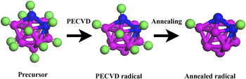
Although the ability to generate semiconducting boron carbide by plasma-enhanced decomposition of carboranes permits the development of high-temperature boron carbide devices at low temperature, it is necessary to control hydrogen content to improve the properties of these devices. For a-B5C:H thin films deposited by PECVD, it is required to strip the exopolyhedral hydrogen atoms from the precursor molecules to form semiconducting thin films, such as o-B10C2H12 for slightly p-type acceptor and m-B10C2H12 for n-type donor-dominated semiconducting materials.Reference Byun, Hwang, Dowben, Perkins, Filips and Ianno11, Reference McIlroy, Zhang, Dowben and Heskett25, Reference Caruso, Bernard, Xu and Dowben26 Similar to a-Si, it is also necessary to keep a certain hydrogen content in the deposited thin films to passivate the dangling bonds to improve electronic properties. Therefore, there is a tradeoff of hydrogen content for electronic properties of a-B5C:H thin films. It is possible to precisely control the hydrogen content by combining PECVD process with annealing process, as shown schematically in Fig. 1. The hydrogen kinetics during the deposition and the annealing is very important for optimizing the processing conditions and improving electronic properties of a-B5C:H thin films. However, there are hitherto no such data reported for boron carbide thin films deposited by PECVD. In this work, we present the very interesting problem of quantitative determination of the hydrogen concentration in a-B5C:H thin films deposited by PECVD from a single-source precursor and after annealing. And then, we study the kinetics of hydrogen during PECVD and annealing process.
Schematic sketch of process procedures to prepare amorphous boron carbide (a-B5C:H) thin films from a carborane precursor: ortho-B10C2H12. Green ball presents hydrogen atom; blue ball presents carbon atom; pink ball presents boron ball.

II. EXPERIMENTAL
The a-B5C:H thin films were deposited on n-Si (111) substrates by PECVD with a mixture of sublimed o-B10C2H12 and Ar gas. Ar was introduced into the chamber as source gas for the plasma. Simultaneously, a radio frequency (rf) discharge was used to maintain the plasma at a frequency of 13.56 MHz with power of 50 W. The reactor plates were heated up and held at 623 K. The chamber pressure was kept at a dynamic equilibrium pressure of 170 mTorr. Four samples (OG1, OG2, OG4, and OG5) were deposited at different precursor fluxes: 9, 18, 36, and 45 sccm, respectively. The ratios of precursor flux to Ar gas were 0.18, 0.36, 0.72, and 0.9, respectively. Additional four small samples cut from sample OG4 were annealed at 673–973 K under the protection of Ar in a tube furnace for 1 hour at intervals of 100 K with the ramping rate at ∼2.3 K/min and then cooled in the furnace to room temperature. The flow rate of Ar was about 700–800 sccm. The cross section of sample OG5 was used to perform HRTEM experiment on JEOL 2010 TEM machine with the acceleration voltage of 200 kV. Nuclear resonance analysis (NRA), described below, was done at the Ion Beam Laboratory, University at Albany, State University of New York. The energy of 15N beam in NRA was slowly increased in steps of 10 keV for resonance from the beginning energy of 6.36 MeV. The emitted γ rays were detected by bismuth germinate detector. Hydrogen concentration was analyzed using Allprof software at a constant density (2.50 g/cm3) for all samples and calibrated using NRA to measure hydrogen concentration in polystyrene (C8H8)n, in which the hydrogen concentration is 50 at.%.27 To investigate the effect of oxygen on hydrogen removal during the annealing, Rutherford back-scattering spectrometry (RBS) was used to measure the oxygen concentration before and after annealing. RBS was also performed at the Ion Beam Laboratory, University at Albany, State University of New York, with 4He+ beams of 3.04 MeV. The x-ray photoelectron spectroscopy (XPS) was performed in a Physical Electronics 5400 system using monochromatic Mg Kα x-rays (1253.6 eV) at a base pressure of ∼10−10 Torr. The XPS system was calibrated by using an Au sample as a reference. Sputter cleaning of the sample surface was achieved by ∼1 uA/cm2 4 keV Ar+ bombardment.
NRA was used to determine the hydrogen concentration quantitatively and the depth of thin films because hydrogen can be detected by using the following resonance reactionReference Bagley, Aspnes, Adams and Benenson28:

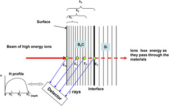
This process is shown schematically in Fig. 2. A 15N+ beam is incident normal to the surface of thin film. Under resonance condition, accelerated 15N+ particles interact with hydrogen atom nuclei, giving off γ rays and other secondary particles. The emitted γ ray at 4.965 MeV is characteristic of this reaction, and the number of γ rays detected at any incident energy is proportional to the hydrogen concentration at the respective depth in the thin film, as shown in the insert in Fig. 2. If 15N+ beam has the correct resonance energy and if it hits hydrogen atoms on the sample surface, γ ray emission will occur. If the hydrogen is below the surface of the sample, 15N+ beam will not generate γ rays unless the beam energy is increased to compensate for the energy reduction of nitrogen beam caused by the interaction with the sample. Therefore, the hydrogen concentration can be determined by measuring the number of γ rays and comparing to a calibrated standard sample. Because the ion beam loses energy constantly and linearly as it passes through the same material, the thickness of a-B5C:H thin films can be calculated by dividing the difference in energy between the resonance energy of 6.385 MeV and the incident beam energy, by the stopping energy.
Schematic representation of measurement of hydrogen concentration and thin film depth-profiling technique using nuclear reaction analysis. Gamma rays result from nuclear reaction between ions and hydrogen atom nuclei, and the yield of γ rays is proportional to the concentration of profiled hydrogen as shown in the insert. E th is the resonance energy that can produce γ rays from hydrogen on the sample surface, whereas E 1, E 2, and E 3 are higher energies required to produce γ rays from hydrogen below the sample surface.

III. RESULTS AND DISCUSSION
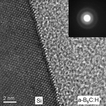
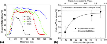
The rectifying I–V curves for boron carbide/n-Si (111) junction indicate that a-B5C:H thin films deposited by PECVD are p-type semiconductors. A HRTEM image of a cross section of a-B5C:H thin film deposited on Si substrate is shown in Fig. 3. The disordered lattice image indicates that no long-range order exists in a-B5C:H thin film, which is confirmed by the diffuse halos of SAD pattern shown in the insert of Fig. 3. Figure 4 shows the effect of o-B10C2H12 flux on the hydrogen concentration in a-B5C:H thin films deposited using PECVD. The ratio of precursor to Ar gas in gas mixture is also shown in Fig. 4. The hydrogen profile in Fig. 4(a) shows that the thickness of OG1, OG2, OG4, and OG5 samples is about 40, 85, 105, and 130 nm, respectively; hydrogen concentration is almost homogenous along the depth of thin films; higher o-B10C2H12 fluxes result in higher hydrogen concentration in the thin films. The resultant higher hydrogen concentration in thin films with the increase in precursor flux can be easily understood. That is, when the precursor flux is higher, the possibility of hydrogen dissociated from the precursor by ions in the plasma is lower after the precursor enters the plasma region and before the PECVD radicals condense into solid state to form thin film. In addition, as shown in Fig. 4(a), the maximum atomic hydrogen concentration in sample OG1 is about 35%, but it is about 45% in sample OG2. The latter brings the hydrogen concentration close to the stoichiometric hydrogen concentration (50 at.%) of the precursor. When the flow rate is 45 sccm, the average hydrogen concentration in sample OG5 is about 50 at.%. The intensity of the B–H peak in the FTIR spectrum also confirmed that hydrogen concentration increases with the increasing precursor flux.Reference Schulz, Lutfurakhmanov, Maya, Sandstrom, Bunzow, Qadri, Bao, Chrisey and Caruso29 It should be noted that hydrogen concentration in sample OG5 at the specific depth of thin film is higher than 50 at.%. It is necessary to review the PECVD process before providing any explanation. The deposition process in PECVD is very complicated because the physical and chemical interactions in the plasma and on the growing film surface are dependent on the rf power and frequency, the substrate temperature, the gas pressure and composition, the magnitude and the pattern of the gas flow, etc. Similar to the process of deposition of a-Si films using a silicon-containing gas, the process of the deposition of a-B5C:H thin films by PECVD could be described in four steps.Reference Schropp and Zeman24 The primary reactions are electron-impact excitation, dissociation, and ionization of precursor molecules. The plasma thus consists of neutral radicals and molecules, positive and negative ion, and electrons. Next, the reactive neutral species move to the substrate by diffusion. After that, surface reactions, such as hydrogen abstraction, radical diffusion, and chemical bonding, occur. Finally, hydrogen molecules are released from the subsurface, and the growing surface relaxes. In addition, B4C and α-boron are considered as inverted molecular crystals because the strength of their intraicosahedral bonds is weaker than that of their intericosahedral bonds.Reference Emin16 Therefore, besides the PECVD radical shown in Fig. 1, it is likely to have other radicals (CxByH1-x-y) due to the breakdown of icosahedrons of the precursor molecules by ions in the plasma. Hydrogen chemisorptions of these radicals could cause the increase of hydrogen concentration in a-B5C:H thin films. Other defects such as voids and porosity, if they exist, also contribute to the hydrogen concentration because hydrogen could be trapped by dangling bonds of these defects. Data fitting, presented in Fig. 4(b), shows that the hydrogen concentration is an exponential function of the precursor flux.
High-resolution transmission electron microscopy image with the insert of selected area diffraction pattern for the a-B5C:H film deposited on Si (111) substrate by plasma-enhanced chemical vapor deposition.

(a) The atomic hydrogen concentration of a-B5C:H thin films under different precursor fluxes and (b) the variation of atomic hydrogen concentration with precursor flux.

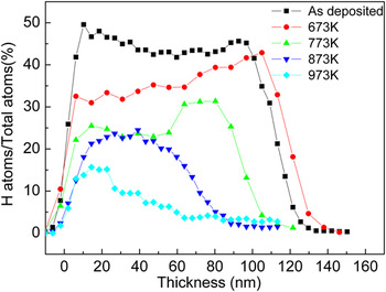
As described before, annealing can be used to control hydrogen concentration and improve the electronic transport of a-B5C:H thin films after deposition. Figure 5 shows hydrogen concentration in a-B5C:H thin films after annealing for 1 h at different temperatures. The average hydrogen concentration decreases with the increasing annealing temperature. Hydrogen removal in a-B5C:H thin films is done in a two-step process during the annealing. The first step is hydrogen dissociation from the PECVD radicals in a-B5C:H thin films. The second is the diffusion of hydrogen atoms to the surface of thin films, where they are carried away by the protection gas. If the former dominates, the kinetics of the removal is said to be reaction controlled. Otherwise, it is diffusion controlled. As shown in Fig. 5, the hydrogen depth profiles of as-deposited thin film and the samples annealed at 673 and 773 K have similar and near flat shapes, which implies that the diffusion of hydrogen atoms toward the sample surface is faster than that of hydrogen dissociation from PECVD radicals in the thin film. Therefore, hydrogen removal is dominated by the dissociation during the annealing, and the kinetics of hydrogen removal is reaction controlled.
The atomic hydrogen concentration of as-deposited a-B5C:H thin film and a-B5C:H thin films annealed at different temperatures.

The process of thermal dissociation of hydrogen in the a-B5C:H thin films can be described by

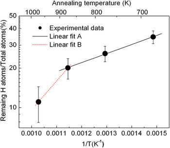
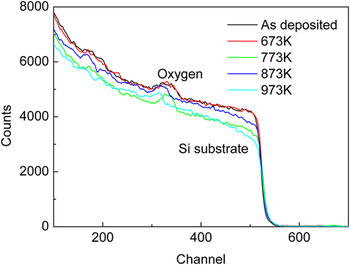
where Z is the hydrogen concentration in the thin films, Q is the activation energy to dissociate hydrogen from either B–H bonds or C–H bonds, A is a constant, k is the Boltzmann constant, and T is the temperature in Kelvin. Figure 6 shows the plot of the logarithmic hydrogen concentration versus the reciprocal of the temperature. It can be seen that there is a linear relationship between the logarithmic hydrogen concentration in the thin films and the reciprocal of annealing temperature from 673 to 873 K with the activation energy of about 0.14 eV, calculated from the slope of the fitted line A. But, hydrogen concentration in the film annealed at 973 K deviates slightly from the linear relationship. The estimated activation energy from fitted line B is ∼0.44 eV in the temperature range from 873 to 973 K. As shown in Fig. 7, RBS spectra indicate no change for the oxygen concentration (∼14%) in the thin films after the annealing, which rules out the effect of oxygen on the hydrogen dissociation during the annealing. Theoretically, if each of the C atoms in the icosahedron is bonded to hydrogen atom, the hydrogen concentration would be 16.7 at.%, which is very close to the maximum hydrogen concentration (15.7%) of thin film annealed at 973 K. In combination with the activation energy, this indicates that hydrogen atoms are dissociated from C–H bonds at higher temperature but from B–H bonds at lower temperature. Additional evidence is that the energy of C–H bond is higher than that of B–H bondReference Sneddon30; the C–H bond length is shorter than B–H bond length.Reference Baughman31 Therefore, the activation energies for hydrogen dissociation from B–H bonds below 873 K and from C–H bonds above 873 K in the a-B5C:H thin films are 0.14 and 0.44 eV, respectively.
The relationship between average remaining hydrogen concentration in the annealed thin films and the annealing temperature.

Rutherford back-scattering spectrometry spectra for as-deposited a-B5C:H thin film and the a-B5C:H thin films annealed at different temperatures.

The insert in Fig. 2 shows the relationship between the thin film depth and hydrogen concentration profile. The thickness of the films, as measured by NRA and shown in Fig. 4, decreases with increasing annealing temperature, which was confirmed by scanning electron microscopy observation. There are two possible reasons that could lead to the decrease in thickness of the thin film after the annealing. One is that the thin film becomes denser when some hydrogen atoms are removed after the annealing because hydrogen concentration is determined from NRA with the assumption that the density of thin films is not changed after the annealing. The other is that the possibility of evaporation of B5CHx during the annealing decreases the thickness of the films.
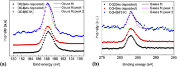
The high-resolution XPS spectra of B1s and C1s core levels obtained for as-deposited and annealed a-B5C:H thin films are shown in Fig. 8. To remove the surface boron–carbon-oxide and surface contaminant, the surfaces of all samples were precleaned by Ar+ beam bombardment. It can be seen that there is no obvious difference for both B1s and C1s spectra between sample OG2 and sample OG4. The single and strong peaks of B1s and C1s spectra for these two samples are located at 188.4 and 283.2 eV, respectively. Therefore, it can be inferred that the binding energies of B1s and C1s for B–H bonds and C–H bonds fall into the similar binding energy range to B–C bonds in boron carbide. In contrast, both B1s and C1s spectra of annealed thin film (OG4) show a dominant peak with a very small shoulder at higher binding energy. These dominant peaks and the shoulders are deconvoluted by Gauss distribution curves. As shown in Fig. 8(a), the Gauss fit of B1s core level shows that a dominant peak is centered at 188.3 eV with the small shoulder at 189.5 eV. The shoulder could be related to B–C bondsReference Jacobsohn, Schulze, Maia da Costa and Nastasi32 in certain chemical environment after hydrogen dissociation from the as-deposited thin film. It is believed that both B1s and C1s spectra are composed of several different intrinsic chemical states of boron carbide originated in its quite complex structure that presents several nonequivalent sites such as intraicosahedral sites and intericosahedral sites.Reference Bao and Chrisey20 Similarly, the Gauss fit of C1s core level shows that a dominant peak is located at 283.2 eV with the small shoulder at 285.2 eV. The binding energy of 285.2 eV is related to C–C bonds.Reference Jacobsohn, Schulze, Maia da Costa and Nastasi32 The close ratio of C1s intensity to B1s intensity for as-deposited thin film and annealed thin film indicates that the thickness of the films after annealing could be caused by the evaporation of B5CHx.
The x-ray photoelectron spectroscopy spectra of (a) B1s core level and (b) C1s core level for as-deposited and annealed a-B5C:H thin films.

IV. CONCLUSIONS
The hydrogen concentration of a-B5C:H thin films deposited using PECVD and after annealing was characterized by nuclear reaction analysis. The hydrogen concentration of the deposited a-B5C:H thin films using a single-source precursor is 35 to 50 at.%. The hydrogen concentration in the a-B5C:H thin films increases exponentially with the increasing precursor flux and could be higher than the stoichiometric hydrogen concentration of the precursor. Annealing is also an effective process to control the hydrogen concentration. After annealing, the hydrogen concentration in a-B5C:H thin films decreases with the increasing annealing temperature. The kinetics of hydrogen removal during annealing is controlled predominantly by its dissociation from PECVD radicals in the deposited thin film. The activation energy of about 0.14 eV is used to dissociate the hydrogen atoms from the B–H bonds, but higher energy (0.44 eV) is required to strip the hydrogen atoms from the C–H bonds. The binding energies of B1s and C1s core levels for B–H bonds and C–H bonds fall into the similar binding energy range for B–C bonds in boron carbide.
ACKNOWLEDGMENTS
The authors wish to thank Dr. Antony N. Caruso and Dr. Joseph Sandstrom at North Dakota State University for the preparation of thin films. The authors are also grateful to Dr. Art Haberl at the Ion Beam Laboratory, University of Albany, State University of New York, for helpful discussion.