I. INTRODUCTION
Today's mobile communication infrastructure demands for high flexibility, low cost, and high efficiency [Reference Lanzani, Kardaras and Boppana1]. As a consequence, the radio frequency (RF) power amplifier (PA) as the most power consuming part in the transmitter architecture needs to be optimized further. Several solutions applying analog PA concepts [Reference Tuffy, Zhu and Brazil2, Reference Mahmoud Mohamed, Boumaiza and Mansour3] have been used for this purpose in the last years.
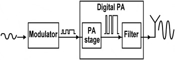
At the same time, there is a clear trend towards complete digital transmitter architectures [Reference Hori4] in order to enhance multi-band capabilities of the hardware, improve compactness, and reduce cost. In this regard, digital PA concepts like class D amplifier or class S amplifier (D/S) have proven to be good candidates [Reference Hori4, Reference Wentzel and Heinrich5]. Figure 1 illustrates the block diagram of such a digital PA. The signal to be transmitted is encoded in a binary pulse sequence and amplified. The analog signal is restored by a filter after the PA only.
Block diagram of digital PA.

A particular challenge for these amplifiers is the design of the reconstruction filter. Stringent requirements in terms of reduced insertion loss, high selectivity, broadband input impedance behavior, and compactness must be fulfilled. Table 1 collects the full specifications of the PA to be designed in this work. In addition, a very compact (typically 50 × 50 × 20 mm3) and efficient design is desired, but without any specified values as the targeted PA approach is the first of its kind in the digital regime. Moreover, at the input, it is operated in a non-50 Ω environment, in order to present optimum termination impedance to the final stage of the PA over a multi-octave bandwidth (BW). Several filter designs have been presented in the last years for this purpose, mainly very simple lumped-element output circuits with poor selectivity [Reference Hori4–Reference Li and Vandewege7] or high insertion loss [Reference Wang, Thiel and Negra8].
Complete specifications of the PA to be designed in this work.

However, lumped-element filters with more complex topologies have also been proposed to synthesize, for instance, dual-band responses [Reference Joshi and Chappell9]. This shows that complex lumped-elements filters could be useful for microwave applications. As alternatives to lumped-elements filters, large-size high-Q combline filters [Reference Serebryakova10] with relatively long connection lines to the PA output have been reported.
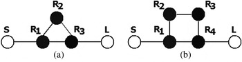
This paper investigates, to the authors’ knowledge for the first time, the design of higher-order lumped-element filters for this purpose, which are highly selective but maintain compactness. The designs target the voltage-mode class-D/S final-stage topology and are based on the trisection and quartet topology shown in Fig. 2. The synthesis, design, and characterization of the quartet lumped-element filter advances this paper compared with the work published in [Reference Martinez-Mendoza11]. The focus is on a compact solution because a short connection between PA output and filter input is strictly required in order to prevent impedance transformations which strongly affect digital PA performance. Results demonstrate that considerable improvement in PA efficiency can be obtained using these alternative topologies, instead of the simpler structures employed in the past.
Coupling schemes explored in this work; (a) trisection topology, (b) quartet topology.

II. SYNTHESIS AND DESIGN CONSIDERATIONS
In this section, the synthesis and design of a trisection lumped-element filter and of a quartet lumped-element filter (see topologies in Fig. 2), suitable for PA operation will be detailed.
In both cases, the design target is a filter with a maximum equiripple BW of 300 MHz maximum with an input return loss of 20 dB and a center frequency of f c = 800 MHz. The designed filter should realize a real input impedance value of 40 Ω within the BW which corresponds to the optimum output impedance of the GaN HEMTs in the final PA stage. Outside the desired BW input impedance should be close to an open circuit to ensure proper low-loss PA operation. This is a non-trivial task when high selectivity is required and the topology is different from the inline version. In the following two subsections we show how these goals can be effectively achieved with the design strategy proposed.
At this point it is important to note that the theory applied in the design strategy is only accurate for narrow band prototypes (with relative BWs of up to 10%) [Reference Cameron12, Reference Cameron, Mansour and Kudsia13]. In our case the specifications require filters with a fractional BW of 37%. Consequently, the synthesis process will produce filter prototypes which will not be perfectly tuned. However, they can be used as initial designs in a subsequent optimization process. In general, we found that the initial designs are quite close to the final circuits, so simple gradient based techniques proved to be very effective for the optimization processes.
A) Lumped-element trisection filter
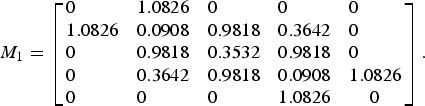
First, our design consists of a third-order filter with 20 dB return loss exhibiting one transmission zero located at the right side of the passband (ω = −3 in the lowpass prototype domain). Using the synthesis technique presented in [Reference Cameron12], the coupling matrix for this filter is found to be:
 $${M_{1}} = \left[ {\matrix{ 0 \hfill & {1.0826} \hfill & 0 \hfill & 0 \hfill & 0 \hfill \cr {1.0826} \hfill & {0.0908} \hfill & {0.9818} \hfill & {0.3642} \hfill & 0 \hfill \cr 0 \hfill & {0.9818} \hfill & {0.3532} \hfill & {0.9818} \hfill & 0 \hfill \cr 0 \hfill & {0.3642} \hfill & {0.9818} \hfill & {0.0908} \hfill & {1.0826} \hfill \cr 0 \hfill & 0 \hfill & 0 \hfill & {1.0826} \hfill & 0 } }\right].$$
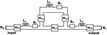
It is well known that such a coupling matrix represents a lowpass circuit filter that can be expressed in its parallel or series configuration [Reference Cameron, Mansour and Kudsia13]. At this point it is important to note that for the targeted voltage-mode class-D/S PA, the series circuit configuration (i.e. using impedance inverters and series resonators as shown in Fig. 3) must be used as starting point for the transformation process. This is essential because the parallel configuration exhibits an out-of-band impedance behavior unsuitable for the power amplifier.
Trisection lowpass filter configuration, based on impedance inverters and series inductor elements.

The next step consists of denormalizing the unitary source/load impedance values (R S = R L = 1), by scaling them to the inverse of their final required values (R S = 1/40 Ω and R L = 1/50 Ω). This can be easily achieved by scaling the value of the first and last inverters accordingly. It is well known that any element R i, Mij, and L i, of a network as the one shown in Fig. 3 can be scaled to new values R i′, Mij′, and L i′, as long as the normalized impedance inverters K ij remain constant:
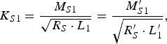 $$K_{S1} = \displaystyle{{M_{S1}} \over {\sqrt {R_S \cdot L_1}}} = \displaystyle{{M_{S1}^{\prime}} \over {\sqrt {R_S^{\prime} \cdot L_1^{\prime}}}}, $$
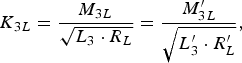 $${K_{3L}} = \displaystyle{{{M_{3L}}} \over {\sqrt {{L_3} \cdot {R_L}}}} = \displaystyle{{{M_{3L}^{\prime}}} \over {\sqrt {{L}^{\prime}_3 \cdot {R}^{\prime}_L}}}, $$
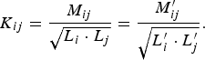 $${K_{ij}} = \displaystyle{{{M_{ij}}} \over {\sqrt {{L_i} \cdot {L_j}}}} = \displaystyle{{{M_{ij}^{\prime}}} \over {\sqrt {{L}^{\prime}_i \cdot {L}^{\prime}_j}}}. $$
Note that the values of the frequency-invariant reactances B i must also be adjusted with the new value of its associated inductor B i′ = M ii × L i′.
At this point, the first and last inverters (M S1, M 3L) may be removed. First we scale them to unity, and next we remove them by inverting the values of R S and R L to obtain the final right source/load impedances (R S = 40 Ω and R L = 50 Ω). The strategy presented here to remove the input/output inverters is much more convenient than the classical approach based on representing these inverters with two reactance elements. Using the classical two reactance elements approach, the equivalence is achieved at the center frequency, and rapidly degrades for large BWs. On the contrary, the approach proposed here is valid for all frequencies, leading to a better response for broadband designs.
The scaling of the input/output inverters to unity will also change the values of L 1 and L 3, which simultaneously determine the value of the inverter M 13. Note that the inductor L 2 can be fixed to any value as long as relation (4) holds, giving us some flexibility. Once L 2 is fixed, inverters M 12 = M 23 will also be fixed.
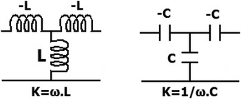
Now, the inductive elements in the lowpass prototype must be transformed to series LC resonant circuits in the bandpass filter and, subsequently, the remaining inverters must be substituted by equivalent lumped-element sections with the circuits shown in Fig. 4.
Impedance inverters equivalence.

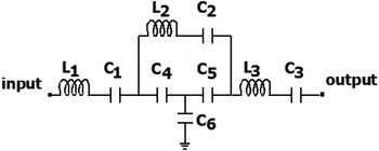
It is important to note that this last task is not simple. These equivalent sections show lumped-elements with negative values, which have to be absorbed by other positive elements in the filter. Thereby, not all solutions are physical. On the other hand, the free choice of the M 12 inverter value and the selection of the L or C equivalent inverter model for each inverter (see Fig. 4) offer degrees of freedom. These can be used to obtain a final network with all the component values being positive. Once the negative elements have been absorbed, the frequency-invariant reactances (B i) have to be removed (by changing the inductors value of their associated resonators accordingly). After the whole process, the compact network shown in Fig. 5 is obtained.
Trisection bandpass filter configuration. Element values for the manufactured prototype are as follows: L 1 = 17 nH, L 2 = 16 nH, L 3 = 20 nH, C 1 = 3.9 pF, C 2 = 9.1 pF, C 3 = 3.3 pF, C 4 = 6.2 pF, C 5 = 5.1 pF, and C 6 = 33 pF.

It is important to notice that this procedure provides an initial filter design only which is close to the expected target response. However, due to the large BW of the filter and the frequency dependence of the inverters, the response of the circuit is not completely tuned. Therefore, a final optimization process is applied until the target specifications are reached.
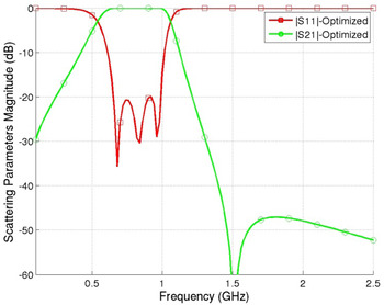
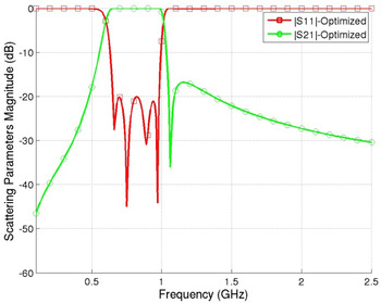
Figure 6 shows the response of the final optimized filter, and the caption collects the optimum element values of the structure. It can be observed good performance of the filter within the passband. The transmission zero is shifted to higher frequencies as compared with the expected response due to the large BW of the prototype. However, the obtained filter is still useful for the intended application. Furthermore, it is important to note that the bond wires (L bond ≈ 0.5 nH) used to connect the PA with the filter as well as the drain-source capacitance (C ds) of the final-stage transistors (C ds ≈ 0.4 pF) were taken into account in a final tuning of the filter. After taking into account all these effects, the element values ready for manufacturing are collected in the caption of Fig. 5.
S-parameters of the trisection filter after applying an optimization process, with 40 Ω reference impedance at the input port and 50 Ω reference impedance at the output port. Optimized elements values according to Fig. 5 are: L 1 = 16.71 nH, L 2 = 14.07 nH, L 3 = 18.93 nH, C 1 = 3.67 pF, C 2 = 9.84 pF, C 3 = 3.08 pF, C 4 = 6 pF, C 5 = 5.52 pF, and C 6 = 27.2 pF.

B) Lumped-element quartet filter
A suitable lumped-element filter of higher-order than the trisection for digital power amplifiers is presented in the following. The higher-order is chosen in order to increase selectivity. Our design consists of a fourth-order filter with −20 dB return loss ideally exhibiting two symmetric transmission zeros located at ω = ±2 in the lowpass domain. Using the synthesis technique presented in [Reference Cameron12], the coupling matrix (5) can be computed.
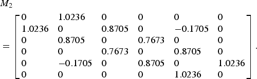 $$\eqalign{&{M_2} \cr &=\left[ {\matrix{ 0 \hfill & {1.0236} \hfill & 0 \hfill & 0 \hfill & 0 \hfill & 0 \hfill \cr {1.0236} \hfill & 0 \hfill & {0.8705} \hfill & 0 \hfill & { - 0.1705} \hfill & 0 \hfill \cr 0 \hfill & {0.8705} \hfill & 0 \hfill & {0.7673} \hfill & 0 \hfill & 0 \hfill \cr 0 \hfill & 0 \hfill & {0.7673} \hfill & 0 \hfill & {0.8705} \hfill & 0 \hfill \cr 0 \hfill & { - 0.1705} \hfill & 0 \hfill & {0. 8705} \hfill & 0 \hfill & {1.0236} \hfill \cr 0 \hfill & 0 \hfill & 0 \hfill & 0 \hfill & {1.0236} \hfill & 0 \hfill } }\right].}$$
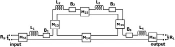
The coupling matrix (5) represents a lowpass circuit filter that can be expressed in its parallel or series configuration [Reference Cameron, Mansour and Kudsia13]. As in the trisection design, in the quartet design it is essential to use the series circuit configuration using impedance inverters and series resonators as starting point for the transformation process since only this configuration, shown in Fig. 7, presents an out-of-band impedance behavior suitable for the targeted PA. Note that the quartet topology can only be implemented if the cross-coupling M 14 is negative, as indicated by the coupling matrix (5).
Quartet lowpass filter configuration, based on impedance inverters and series inductor elements.

A similar strategy as described in the previous example is also applied to the design of the quartet topology. Again, the unitary source/load impedance values (R S = R L = 1) is scaled to the inverse of their final required values (R S = 1/40 Ω and R L = 1/50 Ω). This is achieved by scaling the value of the first and last inverters accordingly. Also, the network shown in Fig. 7 can be scaled to new values R i′, M′ij, and L i′, as long as the normalized impedance inverters K ij stated in (2–4) remain constant. Finally, the frequency-invariant reactances B i should also be adjusted to the new value of its associated inductor. However in this case this step is not needed since the symmetric quartet is a synchronously tuned topology, and therefore all the frequency-invariant reactances B i are null, as indicated by the diagonal of coupling matrix (5).
At this point, the first and last inverters (M S1, M 4L) must again be scaled to unity, and next removed by inverting the values of R S and R L to obtain the final right source/load impedances (R S = 40 Ω and R L = 50 Ω). As in the trisection, this approach is valid for all frequencies, leading to a better response for broadband designs, in contrast to the traditional use of reactance elements to substitute the input and output inverters.
The scaling of the input/output inverters to unity will also change the values of L 1 and L 4, which simultaneously determine the value of the inverter M 14. Note that inductors L 2 and L 3 can be fixed to any value as long as the scalar coupling coefficients k ij remain constant, giving us some flexibility. Once L 2 and L 3 are fixed, inverters M 12, M 34, and inverter M 23 will also be fixed.
Next, the inductive elements in the lowpass prototype must be transformed to series LC resonant circuits in the bandpass filter and, subsequently, the remaining inverters must be substituted by equivalent lumped-element sections with the circuits shown in Fig. 4.
As in the trisection, this last task is not simple, since not all solutions are physical. On the other hand, the free choice of the L 2 and L 3 values and the selection of the L or C equivalent inverter model for each inverter give the designer some degrees of freedom. These allow us to obtain a final network with all the component values being positive. In the particular case of the quartet, inverters M 12 and M 34 have been substituted by their equivalent C inverter models, whereas the inverter M 14 has been substituted by its equivalent L inverter model. This choice is related to the negative sign of this coupling, as shown in the coupling matrix of equation (5). With this strategy, the circuit showed an S-Parameter response close to the ideal one.
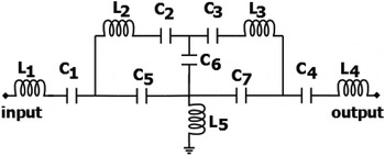
Applying all the detailed circuit transformations to the initial circuit in quartet configuration shown in Fig. 7 yields the final compact network presented in Fig. 8.
Quartet bandpass filter configuration. Element values for the manufactured prototype are as follows: L 1 = 18 nH, L 2 = 11 nH, L 3 = 9 nH, L 4 = 22 nH, L 5 = 1.65 nH C 1 = 2.2 pF, C 2 = 12 pF, C 3 = 33 pF, C 4 = 1.8 pF, C 5 = 6.2 pF, C 6 = 13 pF, and C 7 = 6.2 pF.

The filter obtained through this synthesis process is not completely tuned, due to the large BW of the designed prototype and to the frequency dependence of the inverters. However, the initial design is close to the desired response, and gradient based optimization techniques are applied until the desired specifications are met. Figure 9 shows the final ideal response of the filter, together with the optimum elements values (collected in the caption).
S-parameters of the quartet filter after applying an optimization process, with 40 Ω reference impedance in the input port and 50 Ω reference impedance in the output port. Optimized elements values according to Fig. 8 are: L 1 = 17.21 nH, L 2 = 9.66 nH, L 3 = 8.65 nH, L 4 = 19.59 nH, L 5 = 1.7 nH, C 1 = 2.48 pF, C 2 = 13.13 pF, C 3 = 25.23 pF, C 4 = 2.14 pF, C 5 = 8.12 pF, C 6 = 13.17 pF, and C 7 = 7.7 pF.

It can be observed that the transmission zero on the left side of the passband is missing due to the limitations of the synthesis process for filters with high fractional BW. In spite of this, it will be shown in the next section that the designed filter is still suitable for the amplifier and, as expected, it is more selective than the previous trisection filter. After taking into account for the inductances of the bond wires and the capacitance of the PA transistors as before, the element values ready for manufacturing are collected in the caption of Fig. 8.
III. REALIZATION AND MEASUREMENTS
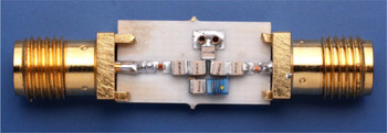
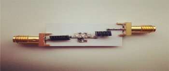
The designed filter circuits (see trisection in Fig. 5 and quartet in Fig. 8) were realized on a 0.51 mm Rogers 4003C printed circuit board (PCB) laminate with a conductor thickness of 36 µm. Figures 10 and 11 show the demonstrators.
Manufactured prototype of the lumped-element trisection bandpass filter; size (w/o connectors): 8 × 14.8 mm2.

Manufactured prototype of the lumped-element quartet bandpass filter; size (w/o connectors): 12 × 24.5 mm2.

For the lumped surface mount device (SMD) inductors, Coilcraft's 0402HP series (Q ≈ 70) was used in both manufactured designs. Moreover, in the case of the quartet, Coilcraft's Low Profile Mini Spring Inductor series (Q ≈ 110), Midi Spring Air Core Inductor series (Q ≈ 135), and Micro Spring Air Core Inductor series (Q ≈ 100) were applied, together with American technical ceramics coorporation (ATC's) 100A series (Q > 200) for the capacitors in both designs.
As the application for these filters are digital microwave PAs, it is important to check the power capability of the proposed designs and its elements. The used lumped-elements can handle DC voltages and currents of higher than 100 V and up to 1 A, respectively. RF-wise the lumped-elements have been tested within other filter designs at the output of PAs in the same frequency range up to peak RF output powers of 15 W. Thus, an output power range of up to 20 W is feasible to be handled with these series of lumped-elements.
A) S-parameters
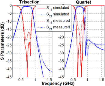
Figure 12 shows the measured S-parameters for the trisection (left) and quartet (right) design, and compares them with the simulated response including losses, and using real models for the lumped-elements around the intended passband range. The quality factors as a model versus frequency can be taken from datasheets of the used lumped-elements, i.e. ATC's 100A and 600L series as well as Coilcraft's 0302CS and 0402HP series. All elements were simulated in advance for the right PCB material (0.51 µm Rogers 4003C) with the modelithics library from DC to 8 GHz. The simulated S-parameters were stored in a data file and used in the filter design as a model. The advantage of this approach is that the full information of the PCB laminate where the elements are mounted on, is included in the model.
Simulated and measured S-parameters of the lumped-element filters; Z in_ref = 40 Ω, Z out_ref = 50 Ω; frequency range: 0.4…1.6 GHz.

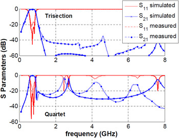
A wider frequency range (0 … 8 GHz) of the S-parameters response is plotted in Fig. 13 to show the broadband filter behavior. Note that the input reference impedance (Z in_ref) for the displayed characteristics is 40 Ω (Z opt of GaN HEMT output stage), while output is referenced to 50 Ω as usual.
Simulated and measured S-parameters of the lumped-element bandpass filters in Fig. 12 for a broad frequency range 0 … 8 GHz.

As can be observed from Figs 12 and 13 good agreement between measured and simulated S-parameters is achieved in the case of the trisection. The realized filter shows an insertion loss and input return loss of 0.8 and 17 dB at f c = 780 MHz, respectively. The transmission zero is located at f = 1.7 GHz and the final equiripple BW is 240 MHz (3-dB BW: 400 MHz). For the quartet design, good agreement is also observed in Figs 12 and 13 between measured and simulated S-parameters, especially around the passband. Far from the passband, the measured results show some spurious not present in the simulated response. This is due to the tolerances of the different lumped-elements used, which show up in the more complex quartet design. Especially the air core inductors (see Fig. 8: L 1, L 4, and L 5), which were not used in the trisection design, involve tolerances which may significantly affect the overall results. Specifically, the tolerances of used lumped-elements vary between ±2 to 10% and ±5 to 10% for capacitors and inductors, respectively. The capacitors are taken from ATC's 100A and 600L series while the 0302CS and 0402HP series from Coilcraft are used for the inductors.
In the case of the quartet, the insertion loss in the measured prototype is 0.75 dB at f c = 755 MHz. This frequency was finally selected, since the measured filter shows an optimum 40 Ω impedance value at this frequency. The transmission zero is located at 1 GHz as it can be observed in Fig. 12 (right), i.e. much closer to the passband than in the trisection and thereby providing a higher selectivity in this region. The final equiripple BW of the quartet is 290 MHz (3 dB BW: 300 MHz). Note that in both designs, i.e. the trisection and the quartet, the 3 dB BW is strongly improved and better controlled as compared with previous lumped-element realizations exhibiting 3 dB BWs of around 700 MHz [Reference Hori4, Reference Wentzel and Heinrich5].
B) Input impedance characteristic
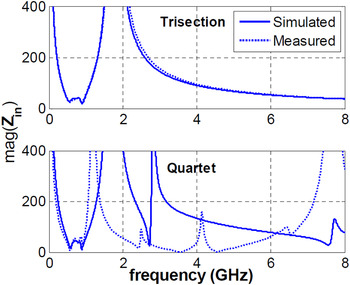
Figure 14 compares simulated and measured input impedance (Z in) behavior of the realized filter structures, since impedance allows a better assessment with regard to the PA output conditions.
Simulated and measured input impedance Z in for the lumped-element bandpass filters; frequency range: 0 … 8 GHz.

In the case of the trisection (Fig. 14, top), the simulated characteristic fits very well with the measured one. More importantly, however, the curves reveal that the filter network provides the optimum Z in of 40 Ω at 780 MHz while in the out-of-band range (down to kHz and up to ≈4 GHz) high impedances beyond 100 Ω are achieved as required.
Furthermore, one should note the small dips (Z in ≈ 30 Ω) in the Z in-characteristic at the lower and upper end of the passband at 550 and 890 MHz. This could influence PA performance when operated with broadband input signals containing frequency components down to kHz and up to several GHz, e.g. bandpass delta sigma modulator (BPDS) or envelope-ΔΣ envelope delta sigma modulation (EDSM) [Reference Hori4]. However, simulations in Agilent's ADS™ with a 1-carrier BPDSM universal mobile telecommunications system (UMTS) input signal (channel BW = 3.84 MHz) show almost no influence for a signal frequency of 780 MHz.
For the quartet filter (Fig. 14, bottom), the specifications in the input impedance behavior around the intended passband range for digital amplifier applications are also fulfilled. Compared with the trisection, the dips appearing in the Z in-characteristic at the lower end of the passband (Z in ≈ 8 Ω at 550 MHz) and at the upper end of the passband (Z in ≈ 10 Ω at 890 MHz) are deeper. But again, in simulation they showed almost no influence on the PA performance. Besides, low impedance values appear from 2 to 7 GHz due to spurious harmonics at these frequencies (see Fig. 13). The reason for that is, as stated already in the last subsection, that the tolerances of the different lumped-elements (especially the air core inductors) have a stronger influence in complex designs like the quartet as compared with the relatively simple trisection approach. The input impedance curve reveals that the filter network provides the optimum Z in of 40 Ω at 755 MHz while in the out-of-band range (down to kHz and up to ≈1.5 GHz) the high impedances (Z in > 100 Ω) are achieved as required for proper amplifier operation.
C) Selectivity check: trisection and quartet filter versus second-order inline
As the focus of this work is on improved selectivity, the influence of the realized trisection and quartet filter on a standard communication signal (1-carrier BPDS-modulated UMTS; crest factor: 6.9 dB) is investigated and compared with a simple second-order inline filter. The inline filter shows similar characteristics to the one in [Reference Hori4, Reference Wentzel and Heinrich5], and it is not described in detail here. Figure 15 shows the measurement setup used for characterization of the filter.
Measurement setup for selectivity check of realized filters including a pattern generator, the filter as the DUT and a spectrum analyzer.

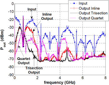
The pulse pattern generator provides the binary bit sequence, the filter structures represent the devices under test (DUT) and the spectrum analyzer displays the spectrum at the filter output. Figure 16 compares the measured BPDS input signal (w/o filter) with the output signals after the manufactured trisection and quartet filters, as well as after the second-order inline filter.
Measured output spectra for a 1-carrier BPDS-modulated UMTS signal: input (w/o filter; dashed blue + points), output with realized trisection (solid black), output with realized quartet (dashed pink) and second-order inline filter for comparison (solid red + crosses).

Above f c (780 MHz) one clearly observes a significant improvement in rejection (maximum +25 dB) when using the realized trisection filter instead of the simple inline design (cp. Fig. 16). This is due to the introduction of a transmission zero in the upper band by the trisection. Below f c the spectra at the output of the two filters (trisection and inline) are comparable.
Regarding the results of the realized quartet filter above f c (780 MHz), a similar rejection to the one obtained with the trisection is observed near the passband, and a considerable improvement around 1 GHz, due to the presence of the transmission zero close to the passband. Above 1.1 GHz the rejection achieved with the quartet filter is lower than with the trisection due to the spurious harmonics of the measured response (see Fig. 13). The reason for the spurious peaks is the higher complexity of the quartet design. Thus element tolerances have a more severe influence, as already described in Section III.A and B. However, below f c (780 MHz) the rejection is considerably improved when using the realized quartet as compared with the rejection obtained with the trisection or the simple inline design.
IV. CONCLUSION
Two compact lumped-element filters for digital microwave PAs (class S or D) in the 800 MHz band have been synthesized, simulated, and successfully realized. The proposed trisection design achieves an insertion loss of 0.8 dB and a minimum input return loss of 17 dB. The realized quartet design shows an insertion loss of 0.75 dB and an input return loss of 10 dB minimum.
Also, both designs fulfil the challenging input impedance requirements, i.e., Z opt = 40 Ω at f c and high Z in (here: >100 Ω) out-of-band down to the kHz-range and up to around 4 GHz in the case of the trisection, and up to 1.5 GHz in the case of the quartet. This deviates from common filter designs but needs to be considered for the special applications targeted in this work, i.e. digital PAs (class-D/S).
Compared with other lumped designs for this type of PAs [Reference Hori4, Reference Wentzel and Heinrich5] the realized filters provide a significantly better controlled BW (3 dB BW: 300 (quartet)/400 MHz (trisection) versus 700 MHz) and higher selectivity. Both designs introduce a transmission zero in the upper frequency band to strongly suppress unwanted frequency components. Besides, the realized quartet achieves a better rejection in the lower band due to the higher-order (number of resonators) as compared with the trisection. Both designs will improve rejection and thus linearity of the targeted class-D/S PAs, which was the focus of this work.
The synthesis process and design approach can be transferred to other filter requirements, for example, in terms of impedance characteristic, BW or frequency bands and thus to other applications. This could be covered in future work.
ACKNOWLEDGEMENTS
The authors would like to thank Alexander von Humboldt Foundation and Federal Ministry for Education and Research of Germany, which has supported this work under a Hildegard Maier Research Fellowship. The work has also been supported by Ministerio de Educación y Ciencia of Spain under grant TEC2013-47037-C5-5-R and European Feder fundings.
 Monica Martinez Mendoza was born in Cartagena, Murcia, Spain, in 1983. She received the Telecommunications Engineer degree from the Technical University of Cartagena (UPCT), Spain, in 2006, and the Ph.D. degree from the same University under the Networking Partnering Initiative (NPI) Initiative with the European Space Agency (ESA), The Netherlands in 2011. Her research topic was synthesis of novel filter topologies for space applications. During November 2011 she worked for 8 months as Postdoctoral Researcher at the Universidad Politécnica of Valencia, with special emphasis on synthesis of multiplexers. Since November 2012 she has been working as Humboldt Postdoctoral Researcher at Ferdinand Braun Institut, Berlín, Germany, focused on the synthesis and design of microwave reconstruction filters for digital power amplifiers.
 Andreas Wentzel received the Dipl.-Ing. and the Ph.D. degree in Electrical Engineering from the Technical University of Berlin, Germany, in 2006 and 2011, respectively. He is presently a post-doc in the microwave department of the Ferdinand-Braun-Institut (FBH) in Berlin, Germany. His research activities focus on the design of digital transmitter architectures including advanced switch-mode power amplifier concepts realized on GaN, especially in class-S and class-D operation, as well as on optimized modulation schemes and filter structures suitable for this type of power amplifiers.
 Alejandro Alvarez Melcon was born in Madrid, Spain, in 1965. From 1991 to 1994 he worked at the European Space Agency (ESTEC) in planar and waveguide filters for satellite applications. From 1995 to 1999 he worked at the Swiss Federal Institute of Technology, Lausanne, Switzerland in planar multilayer microwave circuits and antennas. Since 2000 he is with the Telecommunications School of the Technical University of Cartagena, Spain.
 Wolfgang Heinrich received the Dipl.-Ing., Dr.-Ing. and habilitation degrees in 1982, 1987, and 1992, respectively, all from the Technical University of Darmstadt, Germany. Since 1993, he has been with the Ferdinand-Braun-Institut (FBH) at Berlin, Germany, where he is head of the microwave department and deputy director of the institute. Since 2008, he is also Professor at the Technical University of Berlin. His present research activities focus on MMIC design with emphasis on GaN power amplifiers, mm-wave integrated circuits, and electromagnetic simulation.