I. INTRODUCTION
Over the last two decades there has been intensive study in the field of thermoelectric (TE) materials due to the fact that TE materials can utilize the Seebeck effect to generate electrical power from thermal energy or conversely the Peltier effect to produce solid state cooling by passing a current through the junction of two dissimilar TE materials.Reference Tritt and Subramanian3–Reference Bell5 An advantage of TE materials and devices is that these are solid state processes that operate without any moving parts or chemical reactions. The conversion efficiency of thermoelectricity is primarily evaluated by the dimensionless figure of merit ZT, which is defined as 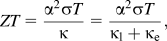 where α, σ, T, and κ are the Seebeck coefficient, electrical conductivity, absolute temperature, and thermal conductivity (including the lattice thermal conductivity κ l and carrier thermal conductivity κ e), respectively. Although there is no known theoretical limit for the ZT value, TE materials with ZT < ∼1 are still relatively rare and furthermore there are no practical useful TE materials that work at very low temperatures, especially in liquid nitrogen range (T < 77 K) to achieve solid state cooling for high temperature superconductors. In addition, very few candidate materials are even remotely available for further investigation of their properties and potential usage at these low cryogenic temperatures.
As a narrow gap, strongly correlated electron semiconductor, FeSb2 single crystals are recently reported to exhibit a huge negative Seebeck coefficient ∼−45,000 μV/K and a record high power factor of 2300 μW/K2-cm at about 10 K, which is 65 times larger than the state-of-the-art Bi2Te3.Reference Bentien, Johnsen, Madsen, Iversen and Steglich1 This colossal Seebeck coefficient is possibly caused by the strong electron correlations among the 3d electrons of Fe and the conduction electrons of Sb, which results in a huge electron density of state near the Fermi level.Reference Bentien, Johnsen, Madsen, Iversen and Steglich1, Reference Bentien, Madsen, Johnsen and Iversen6 However the TE performance of FeSb2 single crystals is restricted by its relatively large thermal conductivity, mostly due to the large lattice thermal conductivity κ l expressed as 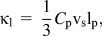 where C p is the specific heat, vs is the sound velocity and l p is the phonon mean free path. The l p of FeSb2 single crystals is approximately two orders of magnitude larger than the electron mean free path l e at about 10 K.Reference Sun, Oeschler, Johnsen, Iversen and Steglich7 On the basis of this large difference between the mean free path of phonons and electrons, we considered that it might be possible to reduce the thermal conductivity by introducing spatially distributed microstructures to scatter the propagating phonons while attempting to maintain the huge power factor in these materials. This dual effect has been achieved previously in some thin filmsReference Sun, Johnsen, Eklund, Sillassen, Bottiger, Oeschler, Sun, Steglich and Iversen8 and melt-spun materials.Reference Xie, Tang, Yan, Zhang and Tritt9 In this work, Sb/InSb nanoinclusions have been able to be formed in situ on the grain boundaries of FeSb2 matrix. It is expected that Sb and InSb, when formed as nanosized inclusions, will induce the desired interface phonon scattering and decrease the lattice thermal conductivity while adding high mobility carriers from the formation of InSb and thus increase the electrical conductivity simultaneously.
II. EXPERIMENTAL PROCEDURES
FeSb2 can be synthesized by several methods.Reference Bentien, Johnsen, Madsen, Iversen and Steglich1, Reference Sun, Oeschler, Johnsen, Iversen and Steglich2 In this work, stoichiometric amounts of Fe, Sb (with an additional 3% excess Sb to compensate for the volatile loss during synthesis process), and indium powders were mixed and rapidly heated to 1050 °C in evacuated quartz tubes, maintained for 2 h, and subsequently quenched in water. Higher purity of the FeSb2 phase can be obtained by annealing at 600 °C in evacuated quartz tubes for 2 weeks. During annealing, it was observed that as the indium content increases, less Sb was found to be deposited on the inside wall of the quartz tubes. Finally, the obtained ingots were pulverized and then sintered by the spark plasma sintering (SPS) (SPS-515S SPS SYNTEX Inc., Kawasaki, Japan) technique at 610 °C for 5 min to obtain highly densified pellets designated as sample numbers 1, 2, 3, and 4 with 0%, 0.5%, 1%, and 3% indium addition, respectively. The relative densities of the resulting polycrystalline samples after the SPS process are all over 97% of the theoretical density of single crystal FeSb2. The crystal structure of the samples after the SPS process was obtained by the x-ray diffraction (XRD; MiniFlex Rigaku/Desktop x-ray diffractometer, Rigaku Corporation, Tokyo, Japan). The micromorphology and chemical composition of the fresh cross sections of the samples after SPS were determined by field emission scanning electron microscopy (SEM; Hitachi S-4800, Hitachi High Technologies America, Inc., Schaumburg, IL) with an energy dispersive x-ray spectroscopy (EDX) option. The thermal conductivity, electrical resistivity, and Seebeck coefficient have been measured from 15 to 300 K on our custom-designed measurement apparatus, and are described in detail elsewhere.Reference Pope, Zawilski and Tritt10, Reference Pope, Littleton and Tritt11 The Hall coefficient and the heat capacity of the various samples were measured on the Quantum Design physical property measurement system (PPMS) (Quantum Design, Inc., San Diego, CA).
III. RESULTS AND DISCUSSIONS
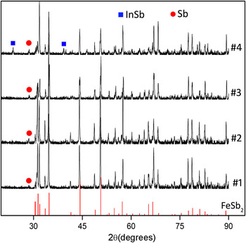
Figure 1 shows the XRD patterns of FeSb2.06 − x% In (x = 0, 0.5, 1, and 3) samples after the SPS process. In addition to the main FeSb2 phases and secondary Sb phase that are indexed, a small trace of InSb phase is detected with the increasing addition of indium and is especially evident in sample number 4. Profile analysis on the XRD patterns shows very close full widths at half maximum for the peaks of FeSb2 in all samples, indicating the particle size distribution of FeSb2 grains is practically the same for all samples.
The x-ray diffraction patterns of the FeSb2.06 − x% In(x = 0, 0.5, 1, and 3) samples after the spark plasma sintering (SPS) process.

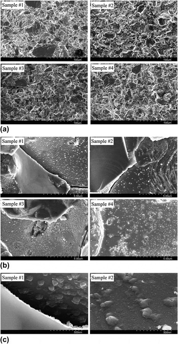
In Fig. 2(a), the low magnification SEM photographs of the cross sections of the samples after SPS show that the crystal grains are distributed randomly within the size range of 5–20 μm. The higher resolution SEM images are presented in Fig. 2(b), showing the uniformly distributed nanoparticles with sizes up to 200 nm, and with the increasing indium addition, the change of the size, shape, and distribution of these nanoinclusions indicates that they differ from sample to sample. In Fig. 2(c), two more detailed SEM images for sample numbers 1 and 2 show that the nanoparticles are distributed evenly on the crystal boundaries and it is apparent that sample number 2 exhibits the finest nanostructures of about 5–10 nm.
(a) The low magnification scanning electron microscope (SEM) images of the cross sections of the samples after SPS, (b) the higher resolution SEM images showing the nanoinclusions, and (c) the more detailed nanostructures of sample numbers 1 and 2.

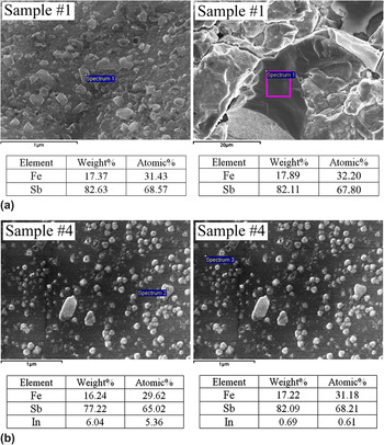
To check the chemical composition of these samples, the EDX analysis was performed on sample numbers 1 and 4 with the results shown in Figs. 3(a) and 3(b), respectively. It can be noted that in sample number 1, the nanoparticles contain an excess of Sb compared with the background matrix. Although this small fluctuation in Sb content is comparable to the uncertainty of the EDX, we still speculate that these nanoparticles in sample number 1 are Sb because of the extra amount of Sb in the starting materials and the Sb secondary phase shown in XRD patterns. In Fig. 3(b), the indium content of the nanoparticle is an order of magnitude larger than that of the matrix background, which is far beyond the EDX resolution limit, indicating that the nanoparticles in sample number 4 are indium rich. Combined with the XRD analysis we can postulate that the InSb nanoparticles are formed in situ on the boundaries of the FeSb2 grains and the composition of the nanoinclusions is alternated from Sb to InSb/Sb with an increasing addition of indium.
(a) The energy dispersive x-ray spectroscopy (EDX) analysis on the sample number 1 cross section, with the spectrum from the nanoinclusion and the smooth grain boundary, and (b) the EDX analysis on the sample number 4 cross section, with the spectrum from the nanoparticle and the background matrix, respectively.

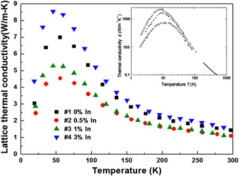
The lattice thermal conductivities of these samples are shown in Fig. 4 with the inset showing the thermal conductivity of the single crystal InSb.Reference Kosarev, Tamarin and Shalyt12 In general, there are three main contributions to the lattice thermal conductivity: (i) boundary scattering, (ii) U-process of phonon scattering, and (iii) mass fluctuation scattering, which dominates at the low-, mid-, and high-temperature ranges, respectively. The low temperature lattice thermal conductivity (at temperatures below the thermal conductivity peak) does not following a monotonic trend. The similar particle size distribution of FeSb2 grains can minimize the effect from the dissimilar grain boundary scattering, whereas the change of the lattice thermal conductivity is more pronounced at low temperatures than high temperatures, which suggests the change in microstructures above the atomic scale should account for this difference. Therefore, we contend that the nanostructures should be the primary cause of the change in the lattice thermal conductivity. With the addition of more indium, the lattice thermal conductivity is first decreased and is then enhanced. The increase of the lattice thermal conductivity can be understood in terms of the large thermal conductivity of the InSb itself,Reference Kosarev, Tamarin and Shalyt12 because more InSb will be formed with a larger indium addition. The sharp drop of the lattice thermal conductivity between sample numbers 1 and 2 may be the result of the increasing amount of in situ formed nanoparticles residing on crystal boundaries, which can then serve to scatter more phonons. Sample number 2 has the lowest lattice thermal conductivity possibly because it possesses both the finest and the broadest size range of nanostructures, which may result in the scattering of phonons over a broader range of wavelengths.
The lattice thermal conductivities of the samples as a function of temperature with the insert showing the thermal conductivities of the InSb single crystals with different carrier concentrations.Reference Kosarev, Tamarin and Shalyt12

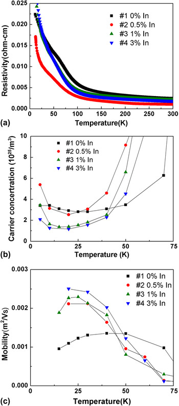
Figure 5 shows the electrical transport properties of all samples. In Fig. 5(a), sample number 2 with 0.5% indium addition shows the lowest electrical resistivity. Figures 5(b) and 5(c) present the Hall carrier concentration and Hall carrier mobility, respectively. It is shown that with the increasing indium addition, the carrier concentration is reduced because of the scattering of the carriers by nanoinclusions. The carrier mobility, however, is enhanced by the formation of InSb, which is known to have one of the largest carrier mobilities amongst several semiconducting materials.Reference Rode13 For sample number 2, the carrier concentration is not degraded significantly, however the carrier mobility is almost doubled, which results in the lowest electrical resistivity among these samples.
(a) The electrical resisitivities as a function of temperature of all the samples, (b) the Hall carrier concentrations as a function of temperature of all the samples, and (c) the Hall carrier mobilities as a function of temperature of all the samples are shown in this figure.

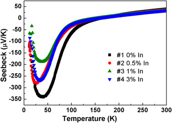
Figure 6 displays the thermopower, or Seebeck coefficient, of all the samples. It is apparent from these results that with the increasing indium content, the peak of the Seebeck coefficient is first suppressed in sample numbers 2 and 3, but then enhanced in sample number 4. This trend is difficult to explain because the Seebeck coefficient of the FeSb2 is anisotropic and extremely sensitive to sample composition, which has previously been reported in the earlier studies of the FeSb2 single crystals.Reference Bentien, Johnsen, Madsen, Iversen and Steglich1, Reference Sun, Oeschler, Johnsen, Iversen and Steglich2 We speculated that the off-stoichiometry and orientations in all the samples may be the cause of the unusual change of the Seebeck coefficients.
The Seebeck coefficients as a function of temperature of all the samples are shown.

IV. CONCLUSION AND FUTURE WORK
A series of FeSb2–Sb/InSb nanocomposite polycrystalline materials were prepared by the traditional solid state reaction method. The in situ formed nanoparticles reside on the crystal boundaries and scatter phonons, which results in a reduction of the thermal conductivity, whereas also enhancing the electrical conductivity via the contribution of high mobility carriers from the formation of the InSb phase. These results exemplified the “phonon glass–electron crystal” approach suggested by Slack.Reference Slack14 Overall, the sample with 0.5% indium addition exhibits the best TE properties among these samples.
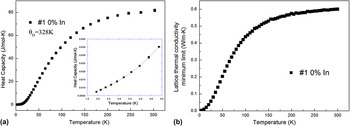
Figure 7(a) shows the low temperature heat capacity of the sample number 1 with the inset showing the curve fitting up to 5 K by the equation of C p=γT + βT3. From the fitting parameter β, the Debye temperature θ D can be calculated as ∼328 K by the equation 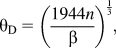 where n is the atom number density.Reference Kittel15 On the basis of the mode proposed by Cahill et al.,Reference Cahill, Watson and Pohl16 the minimum limit of the lattice thermal conductivity is calculated and presented in Fig. 7(b), revealing there is still a possibility for further reduction of the lattice thermal conductivity. In future works, nanostructured FeSb2 samples will be prepared by melt spinning or high-energy ball milling and then combine with nanoparticles targeted for crystal boundaries to achieve a complex multiscale nanocomposite. Also, a further study of the relation between strong electron correlations and Seebeck coefficient of these samples is strongly needed in order that its effect might be distinguished from other correlation effects, such as phonon drag, charge-density waves, and spin-density waves. It seems to be apparent that if these materials are in reality to be used as low temperature TE materials, they will most likely have to be synthesized and understood in their polycrystalline form, otherwise the very large lattice thermal conductivity that exists in the single crystals will ultimately limit their potential.
(a) The low temperature dependence of the heat capacity of the sample number 1 with the inset showing the curve fitting up to 5 K and (b) the minimum limit for the lattice thermal conductivity of sample number 1 with 0% indium.

ACKNOWLEDGMENTS
We thank Dr. Jian He and Dr. Catalina Marinescu in the Department of Physics and Astronomy of Clemson University for their inspired discussions. We would like to acknowledge the financial support from DOE/EPSCoR Implementation Grant (No. DE-FG02-04ER-46139) and SC EPSCoR Office/Clemson University cost sharing.