Introduction
Organic semiconductors form the basis of organic electronics and photonics, fields that are engaged in the development of electronic devices such as flexible, low-cost, disposable electronics, organic solar cells, light-emitting displays, smart tags, and molecular sensors.Reference Forrest1 Despite the rapid recent progress in applied organic electronics and a long history of basic research on organic materials,Reference Silinsh and Čápek2, Reference Pope and Swenberg3 our understanding of the fundamental properties of this important class of semiconductors is still limited. This disparity is mainly rooted in significant disorder that dominates the electrical and optical properties of polycrystalline and amorphous organic thin films, resulting in disorder-limited charge-carrier mobilities and exciton diffusion that complicate attempts to compare experimental results with theory. However, recently developed electronic devices based on single crystals of organic semiconductors, materials with a much higher long-range structural order and chemical purity, now allow experimental access to the intrinsic (i.e., not dominated by disorder and sample morphology) fundamental electronic properties of organic semiconductor devices (see References Reference de Boer, Gershenson, Morpurgo and Podzorov4 and Reference Gershenson, Podzorov and Morpurgo5). Because of this, organic single crystals are now widely recognized as an important tool for the studies of the fundamental charge and energy excitations (polarons and excitons, respectively) and their transport, intrinsic surface, and interfacial phenomena, as well as intrinsic optical properties of organic semiconductors.
This introductory article describes the motivation, a brief history, and the main future goals of the field of organic single-crystal optoelectronics. It also gives an outline of the review articles that follow, including crystallization and patterning methods, device fabrication, measurements of electrical and optical properties, and theoretical modeling. In addition, this article gives a thorough review of different fabrication methods of high-performance single-crystal organic field-effect transistors (OFETs), their electrical characteristics, and intrinsic and trap-dominated transport regimes and an overview of modern theoretical models of electronic properties of organic semiconductors.
The importance of organic single-crystal research stems from several specific benefits that these materials offer in regard to fundamental studies: (1) high structural order (in particular the absence of grain boundaries), (2) high chemical purity, and (3) availability of several efficient methods for fabrication of high-quality semiconductor-dielectric interfaces developed during the past decade. The first two properties have been shown to be very important for observations of band-like transport in photoconductors based on molecular crystals in the pioneering time-of-flight measurements performed by Karl and co-workers.Reference Karl, Farchioni and Grosso6 The last point is especially important for OFETs, wherein the charge-carrier transport occurs at the semiconductor-insulator interface, and thus the quality of this interface has a direct impact on the charge-carrier mobility, μ, the parameter characterizing how fast charge carriers drift in a material in response to an external electric field.Reference Bao and Locklin7 It has been challenging to fabricate these interfaces with a sufficiently low density of defects at the surface of molecular crystals. This difficulty was mainly due to the fragile nature of the surfaces of these materials that are incompatible with the conventional fabrication methods used in inorganic semiconductor processing. Nevertheless, the immense efforts of the organic electronics research community in the early 2000s, directed toward realization of single-crystal OFETs, ultimately resulted in the first successful demonstration of high-performance devices based on single crystals of rubrene in 2002–2003.Reference Podzorov, Pudalov and Gershenson8, Reference Podzorov, Sysoev, Loginova, Pudalov and Gershenson9 This was followed by analogous demonstrations using single crystals of tetraceneReference de Boer, Klapwijk and Morpurgo10, Reference Newman, Chesterfield, Merlo and Frisbie11 and pentacene,Reference Takeya, Goldmann, Haas, Pernstich, Ketterer and Batlogg12–Reference Butko, Chi, Lang and Ramirez14 thus overcoming the fabrication bottleneck in this area. This development has initiated ever-growing activity in organic single-crystal devices with the purpose of exploring fundamental limitations and intrinsic electronic properties of organic semiconductors.
To date, the highest reproducible charge-carrier mobility in organic semiconductors has been achieved in p-type single-crystal rubrene OFETs, wherein, depending on the crystal orientation and the choice of the gate dielectric, the intrinsic hole mobility can reach up to 20 cm2 V–1 s–1 at room temperature.Reference Podzorov, Menard, Borissov, Kiryukhin, Rogers and Gershenson15 This value is much better than the mobility sufficient for a wide range of commercial applications, such as those currently utilizing amorphous silicon (Si) FETs with μ ∼ 1 cm2 V–1 s–1. However, it is much lower than μ in high-purity single crystal Si (∼500 cm2 V–1 s–1) FETs used in commercial high-speed electronics. Among n-type single-crystal OFETs, the best performers seem to be single crystals of N,N′-bis(n-alkyl)-(1,7 and 1,6)-dicyanoperylene-3,4:9,10-bis(dicarboximide) (PDIF-CN2) developed by Facchetti and co-workers and explored by Morpurgo and co-workersReference Molinari, Alves, Chen, Facchetti and Morpurgo16, Reference Minder, Ono, Chen, Facchetti and Morpurgo17 and 5,7,12,14-tetrachloro-6,13-diazapentacene (TCDAP) synthesized and studied by Tao and co-workers,Reference Minarul Islam, Pola and Tao18 in which the room-temperature electron mobility can reach a few cm2 V–1 s–1, about an order of magnitude greater than reproducible μ values obtained in polycrystalline n-type OFETs.
Aside from the demonstrations of high charge-carrier mobilities, growing interest in organic single crystals has already resulted in a series of important fundamental discoveries. These include, for instance, the observation of intrinsic (i.e., not dominated by traps) polaronic transport at the surface of organic semiconductors (i.e., the motion of charge coupled to local lattice distortion),Reference Podzorov, Menard, Borissov, Kiryukhin, Rogers and Gershenson15 an intrinsic structure-property relationship in the form of mobility anisotropy observed experimentallyReference Podzorov, Menard, Borissov, Kiryukhin, Rogers and Gershenson15, Reference Sundar, Zaumseil, Podzorov, Menard, Willett, Gershenson and Rogers19–Reference Ostroverkhova, Cooke, Hegmann, Tykwinski, Parkin and Anthony24 and studied theoretically,Reference Ortmann, Bechstedt and Hannewald25–Reference Wen, Li, Song, Deng, Han and Goddard28 observation of a band-semiconductor Hall effect in molecular solids,Reference Podzorov, Menard, Rogers, Gershenson, Podzorov, Menard, Rogers and Gershenson29–Reference Minder, Ono, Chen, Facchetti and Morpurgo34 and non-activated (band-like) charge transport observed in conductivity measurements,Reference Podzorov, Menard, Borissov, Kiryukhin, Rogers and Gershenson15, Reference Podzorov, Menard, Rogers, Gershenson, Podzorov, Menard, Rogers and Gershenson29, Reference Minder, Ono, Chen, Facchetti and Morpurgo34 as well as in ultrafast optical experiments,Reference Ostroverkhova, Cooke, Hegmann, Anthony, Podzorov, Gershenson, Jurchescu and Palstra35, Reference Tao, Matsuzaki, Uemura, Yada, Uemura, Takeya, Hasegawa and Okamoto36 gate-controlled light emission from ambipolar single-crystal OFETs with a record-high current density (a few hundred A/cm2, which is two orders of magnitude greater than that in conventional organic light-emitting diodes),Reference Takenobu, Bisri, Takahashi, Yahiro, Adachi and Iwasa37 and determination of the intrinsic anisotropic mechanical properties of flexible organic single crystals.Reference Reyes-Martinez, Ramasubramaniam, Briseno and Crosby38 Novel optical phenomena in highly ordered molecular crystals have also attracted much attention in recent years. For instance, interesting processes such as singlet exciton fission (splitting of one exciton into two) and triplet fusion (two excitons combine into one),Reference Smith and Michl39 as well as remarkably long exciton lifetimes (∼100 μs) and diffusion lengths of up to a few μm, give rise to such intriguing phenomena as surface photoconductivity and magnetic field effect on photoluminescence and photoconductivity in high-purity crystals.Reference Najafov, Biaggio, Podzorov, Calhoun and Gershenson40–Reference Muller, Avlasevich, Schoeller, Mullen and Bardeen45
Organic single-crystal growth, patterning, and characterization
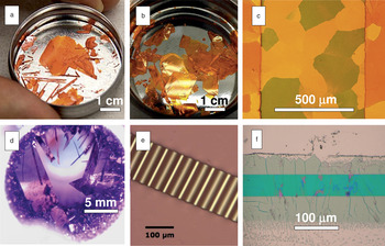
Several methods have been developed for high-purity organic crystal growth: physical vapor transport (PVT) growth of freestanding molecular crystals from a vapor phase in a stream of inert gasReference Laudise, Kloc, Simpkins and Siegrist46 (optimized growth procedures for rubrene can be found in References Reference Bao and Locklin7 and 47), crystallization from solution for growing large crystalline domains along a substrate,Reference Anthony48–Reference Nakayama, Hirose, Soeda, Yoshizumi, Uemura, Uno, Li, Kang, Yamagishi, Okada, Miyazaki, Nakazawa, Nakao, Takimiya and Takeya53 and seeded Bridgman crystallization from meltsReference Niemax, Tripathi and Pflaum54 (Figure 1). Currently, PVT growth provides the best results in terms of the chemical purity, structural order, and the electrical performance of single-crystal devices. The main advantage of this method, besides simplicity, is that molecular impurities are effectively separated due to the temperature gradient created along the growth tube, and thus efficient chemical purification is achieved. Details and analysis of crystal growth from vapor are described in the article by Jiang and Kloc in this issue of MRS Bulletin.
Organic single crystals and crystalline films of popular small-molecule compounds used in organic electronics: (a) Rubrene,4 (b) tetracene,4 (c) 5,11-bis(triethylsilylethynyl)anthradithiophene (TES-ADT) (reproduced with permission from Reference Reference Lee, Kim, Gomez, Purushothaman, Toney, Wang, Hexemer, Anthony and Loo51, © 2009 Wiley), (d) dimethyl-pentacene,Reference Chen, Lee, Yi, Lee, Payne, Pola, Kuo, Loo, Anthony, Tao and Podzorov55 (e) ultrathin sheet of wrinkled rubrene (reproduced with permission from Reference Reference Reyes-Martinez, Ramasubramaniam, Briseno and Crosby38, © 2012 Wiley), and (f) 2,7-dioctyl[1]benzothieno[3,2-b][1] benzothiophene (C8-BTBT) (reproduced with permission from Reference Reference Uemura, Hirose, Uno, Takimiya and Takeya52, © 2009 The Japan Society of Applied Physics). The single crystals in (a), (b), (d), and (e) were grown from vapor; the rubrene sheet in (e) is laminated at the surface of the polydimethylsiloxane stamp. The crystalline films in (c) and (f) are grown from solutions at an SiO2 surface.

While the vapor transport method is well developed and delivers some of the highest order and purity small-molecule organic single crystals, solution growth techniques are perhaps more favorable for applications. Various approaches of organic film growth from solutions resulting in an oriented or spherulitic domain growth along the substrate have been suggested in the literature (Figure 1).Reference Dickey, Anthony and Loo49–Reference Nakayama, Hirose, Soeda, Yoshizumi, Uemura, Uno, Li, Kang, Yamagishi, Okada, Miyazaki, Nakazawa, Nakao, Takimiya and Takeya53 The patterned growth of organic single crystals on substrates from vapor and solution deposition methods are covered in this issue in the article by Li et al.
Structural order, chemical purity, and stability of single-crystal organic semiconductors
Besides grain boundaries, other types of disorder are usually minimized or avoided in freestanding organic single crystals. Currently, the organic semiconductor with the highest degree of order and purity is single-crystalline rubrene that forms large orthorhombic single crystals with typical dimensions of 1–10 mm. Rubrene can be grown in a variety of morphologies, ranging from thick and bulky robust crystals to ultrathin (0.2–1 μm) flexible crystalline sheets (Figure 1). The bulky crystals can be easily handled and used in fabrication of freestanding devices.8,9 The ultrathin crystals can be electrostatically attached (laminated) to substrates such as SiO2 or flexible plastics. This property of ultrathin crystals was utilized by Briseno and co-workers in developing flexible single-crystal rubrene OFETs on Kapton (a thin insulating plastic substrate), with outstanding electrical performance (μ ∼ 5 cm2 V–1 s–1), that can be bent to a radius of R ∼6 mm without degradation of electrical properties.Reference Briseno, Tseng, Ling, Falcao, Yang, Wudl and Bao56 Rubrene exhibits unprecedented, high structural order in the bulk with extremely narrow peaks in x-ray rocking curves characterized with an angular width (x-ray mosaic spread) of just 0.016°. This is a factor of five smaller than in the best molecular crystals reported previously, as revealed in the recent studies of Siegrist and co-workers.Reference Zeis, Besnard, Siegrist, Schlockermann, Chi and Kloc22 The surface of rubrene is also highly ordered: It exhibits large molecular terraces (low density of molecular steps) that can have widths as large as ∼10 μm in high-quality crystals, with an average crystal typically showing ∼1 μm-wide terraces.Reference Lee, Choi, Cheong and Podzorov57, Reference Ellison, Lee, Podzorov and Frisbie58
The low density of defects makes organic single-crystal devices much more stable against degradation as compared with their polycrystalline analogs. For instance, the dense molecular packing at the surface of rubrene makes its surface highly resistant to oxidation, even when the samples are stored in air. The high surface purity and high carrier mobility in rubrene help avoid detrimental surface charging in scanning tunneling microscopy (STM) measurements, which resulted in the first molecular-resolution STM images of as-grown (uncleaved) surface of bulk organic crystals, confirming that the surface of high-quality crystals indeed remains unoxidized.Reference Menard, Marchenko, Podzorov, Gershenson, Fichou and Rogers59 Recent demonstrations of selective decoration of molecular steps at the rubrene surface with silane self-assembled monolayers,Reference Lee, Choi, Cheong and Podzorov57, Reference Ellison, Lee, Podzorov and Frisbie58 as well as morphological changes in the molecular steps observed with atomic force microscopy,Reference Thompson, Yadin, Grout, Hudziak, Kloc, Mitrofanov and Curson60 also suggest that only molecular steps are oxidized in these crystals. It is worth mentioning that high surface quality is also crucial for successful application of ultraviolet photoelectron spectroscopy (UPS) techniques to macroscopically thick (∼0.1–3 mm) organic single crystals, necessary to resolve their electronic band structure.Reference Nakayama, Machida, Minari, Tsukagoshi, Noguchi and Ishii61, Reference Machida, Nakayama, Duhm, Xin, Funakoshi, Ogawa, Kera, Ueno and Ishii62
Understanding the fundamental mechanisms of oxidation and formation of related trap states using organic single crystals, specifically rubrene, as model systems is very important for addressing environmental and operational stability of organic semiconductors. For instance, recent electrical measurements of rubrene single crystals have revealed that the purest crystals can have a density of deep traps as low as 1015 cm–3, yet oxidation leads to a much higher density of deep traps peaking at ∼0.27 eV off the highest occupied molecular orbital (HOMO) band edge, resulting in a reduction in the electrical conductivity of the crystals.Reference Krellner, Haas, Goldmann, Pernstich, Gundlach and Batlogg63 More recently, studies of photo-oxidation effects on the optoelectronic properties of rubrene have revealed that as long as the crystals are stored in the dark, their surface remains unoxidized, even if the crystals are stored in air or pure oxygen.Reference Najafov, Mastrogiovanni, Garfunkel, Feldman and Podzorov64 However, illumination in an oxygen atmosphere with intense white light triggers surface photo-oxidation and persistent oxygen diffusion into the bulk at length scales comparable to the light penetration length (1–5 μm in the visible range of the spectrum).Reference Najafov, Mastrogiovanni, Garfunkel, Feldman and Podzorov64 Remarkably, oxidation results in qualitative changes in the photo-current excitation spectra of the crystals, converting the so-called “normal” modulations of photoconductivity in pristine crystals to “anti” modulations in trap-dominated ones, thus providing a simple diagnostic method for crystal purity. In prior spectroscopic studies, it was suggested that oxygen impurities in rubrene create a distinct photoluminescence (PL) band, red-shifted with respect to the main PL peak of crystalline rubrene.Reference Mitrofanov, Lang, Kloc, Wikberg, Siegrist, So, Sergent and Ramirez65, Reference Mitrofanov, Kloc, Siegrist, Lang, So and Ramirez66 However, another recent study suggests that such a band may appear as a result of a very small amount of structural disorder in the crystals, rather than being induced by oxidation.Reference Chen, Lee, Fu and Podzorov67 The lack of agreement between different experiments on spectroscopic signatures of oxidation even in the case of well-characterized and highly ordered crystalline rubrene indicates the complexity of this important problem and the challenge we face in its understanding.
Fabrication of high-performance single-crystal OFETs
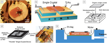
The success of single-crystal organic electronics is due in part to our ability to create high-quality interfaces between organic crystals and dielectrics, such as a variety of plastic insulators or SiO2. Single-crystal organic field-effect transistors can be classified by the method used for fabrication of this interface (Figure 2). Some of the first high-performance single-crystal OFETs were created using a parylene conformal coating—a technique resulting in an organic crystal uniformly coated with an ultrathin layer of a robust and stable plastic dielectric (parylene). This method works very well for most organic crystals: It results in trap-free interfaces, provides a dielectric coating with excellent breakdown characteristics, can be used to coat sharp crystal edges and rough surfaces without pinholes, and can be applied to crystals of any shape and morphology.8,9,14,18,22 In addition, parylene is transparent in the visible range of the spectrum, which is crucial for optical experiments with OFETs.Reference Podzorov and Gershenson68, Reference Calhoun, Hsieh and Podzorov69 Parylene deposition is inexpensive and easy to set up (details can be found in Reference 47). Another popular method of single-crystal OFET fabrication is electrostatic bonding of organic crystals to either hard or soft “transistor stamps”—pre-fabricated FET structures made using either doped-Si/SiO2 wafers (hard stamps)Reference de Boer, Klapwijk and Morpurgo10–Reference Takeya, Nishikawa, Takenobu, Kobayashi, Iwasa, Mitani, Goldmann, Krellner and Batlogg13 or a rubber-like polydimethylsiloxane (PDMS) material (soft stamps).Reference Podzorov, Menard, Borissov, Kiryukhin, Rogers and Gershenson15, Reference Minder, Ono, Chen, Facchetti and Morpurgo17, Reference Sundar, Zaumseil, Podzorov, Menard, Willett, Gershenson and Rogers19, Reference Reese and Bao20, Reference Menard, Podzorov, Hur, Gaur, Gershenson and Rogers70 The most important advantage of this method is that complicated contact geometries are possible through the use of lithography. The main disadvantage is that only very thin and bendable crystals can be electrostatically attached to hard Si/SiO2 wafers, while air-gap PDMS transistor stamps normally require rigid and robust crystals with very flat and uniform surfaces.
Different approaches to fabrication of single-crystal organic field-effect transistors (OFETs). (a) A high-mobility freestanding rubrene OFET with a conformal parylene gate dielectric, wired to a sample holder.8,9 (b) “Air-gap” or “vacuum-gap” single-crystal OFETs based on soft polydimethylsiloxane (PDMS) transistor stamps, in which an undesirable interaction of the dielectric with a clean surface of the crystal is avoided due to the separation of the recessed gate electrode from the conduction channel by a few μm-thick gapReference Podzorov, Menard, Borissov, Kiryukhin, Rogers and Gershenson15, Reference Menard, Podzorov, Hur, Gaur, Gershenson and Rogers70 (reproduced with permission from Reference Reference Menard, Podzorov, Hur, Gaur, Gershenson and Rogers70, © 2004 Wiley). (c) Single-crystal OFETs based on hard Si/SiO2 structures with evaporated contacts and an electrostatically attached thin single crystalReference de Boer, Klapwijk and Morpurgo10, Reference Takeya, Goldmann, Haas, Pernstich, Ketterer and Batlogg12 (reproduced with permission from Reference Reference Takeya, Goldmann, Haas, Pernstich, Ketterer and Batlogg12, © 2003 American Institute of Physics). (d) Mechanically flexible single-crystal OFETs on Kapton substrates with a polymer gate dielectric (PVP) (reproduced with permission from Reference Reference Briseno, Tseng, Ling, Falcao, Yang, Wudl and Bao56, © 2006 Wiley). (e) Single-crystal OFETs using a thin, freestanding plastic membrane laminated against the surface of a crystal by vacuum (gate is not shown) (reproduced with permission from Reference Reference Yi, Chen, Czelen and Podzorov71, © 2011 Wiley). Note: S, source; D, drain; G, gate; OTS, octyl trichloro-silane; PET, polyethylene terephthalate; PVP, polyvinylpyrrolidone; ITO, indium tin oxide.

Finally, a very simple yet efficient new method, utilizing vacuum lamination of ultrathin dielectric membranes on top of organic crystals, has been recently developed.Reference Yi, Chen, Czelen and Podzorov71 In this method, a freestanding few μm-thick plastic film (gate dielectric membrane) is gently applied to the crystal’s surface under vacuum, thus eliminating the deleterious effects of harsh chemical or physical processes, such as those frequently encountered in chemical vapor deposition, atomic layer deposition, high vacuum, or plasma-based techniques. This preserves high-quality single-crystal surfaces. Besides its nondestructive nature, this method is the first reversible method of gate dielectric formation: releasing the vacuum causes the gate dielectric film to pop up, leaving the pristine crystal surface without damage or degradation and ready for further experiments. Thus, other gate dielectric membranes (consisting of different dielectric materials or functionalized at the surface with, for example, various self-assembled monolayers or nanoparticles) can be sequentially applied to the same organic single crystal. The nondestructive nature and reversibility of the membrane lamination eliminates parameter variability and large scatter in the data collected on different crystals. This technique is thus important for conducting more accurate, fundamental characterization of organic/dielectric interfaces.Reference Yi, Chen, Czelen and Podzorov71
A separate category of single-crystal OFETs are the electrolyte-gated devices, in which field effect is achieved by using ionic liquids that act as a gate and a dielectric at the same time.Reference Xia, Xie, Ruden and Frisbie72, Reference Shimotani, Asanuma, Takeya and Iwasa73 Application of a small gate voltage to the electrolyte results in the accumulation of solvated ions (i.e., ions capped with solvent molecules) near the surface of an organic crystal, creating a Helmholtz double layer with a very high density of mobile holes (1013–1015 cm–2). The Helmholtz double layer can be viewed as a capacitor that consists of a layer of ions and a layer of oppositely charged charge carriers, the two separated by a nanoscale distance, thus resulting in a very large capacitance per unit area. These devices are indispensable for studies of the high carrier density regime in organic semiconductors.Reference Xia, Xie, Ruden and Frisbie72, Reference Shimotani, Asanuma, Takeya and Iwasa73 Studies of a high carrier density transport regime in electrolyte-gated organic single crystals are covered in this issue in the article by Xie and Frisbie.
Electrical characteristics of single-crystal OFETs
An important advantage of single-crystal OFETs is that their electrical characteristics typically follow the theoretical FET behavior derived using Shockley’s gradual channel model.Reference Sze and Ng74 This facilitates accurate experimental determination of charge-carrier mobility. The model relates the channel conductivity per square, σ, the charge-carrier mobility, μ, and the gate voltage, V G, and is based on the following assumptions: (1) μ does not depend on the carrier density, n, in the channel; (2) Ohm’s law and the Drude model of conductivity are applicable (i.e., σ can be expressed through the source-drain current, I SD, and the source-drain voltage, V SD, as σ = (I SD/V SD)·(L/W), where L and W are the length and width of the OFET’s accumulation channel, respectively), and σ is proportional to the product of carrier density and mobility, σ = enμ (e = 1.6 × 10⁻¹⁹C is the electron charge); (3) at any position along the accumulation channel, the longitudinal electric field is much smaller than the local gate (transverse) electric field (the so-called graduate channel approximation); and (4) Schottky contact resistance is much smaller than channel resistance. The last condition is very important for the most commonly used two-probe OFET configuration comprising two contacts and a gate electrode; it ensures that the apparent mobility determined in a two-probe OFET is not significantly affected by the parasitic contact resistance. If the contact resistance is significant (or unknown), a four-probe OFET configuration must be used to separately measure the channel and the contact resistances. Four-probe measurements in organic transistors were carried out first in rubrene single crystals,8 and subsequently the method was applied to other materialsReference Newman, Chesterfield, Merlo and Frisbie11, Reference Takeya, Goldmann, Haas, Pernstich, Ketterer and Batlogg12, Reference Merlo and Frisbie75, Reference Chesterfield, Mckeen, Newman, Frisbie, Ewbank, Mann and Miller76 (details of the four-probe OFET technique can be found in Reference Reference Bao and Locklin7).
The Shockley FET model leads to a linear relationship between the channel source-drain current in the linear regime (I SDlin) and the gate voltage (this regime is realized at |V G| >> |V SD|, when the carrier density distribution along the channel is nearly constant), and it leads a quadratic dependence of the source-drain current (I SDsat) in the so-called saturation regime (realized at |V G| < |V SD|, with a highly non-uniform carrier density distribution that has a pinch-off (carrier depletion) near one of the contacts):
 $$I_{SD} ^{lin} = {W \over L}{\rm{\mu }}C_i V_D (V_G - V_T)\,(\left| {V_G } \right|\, > > \,\left| {V_{SD} } \right|)$$
 $$I_{SD} ^{sat} = {W \over {2L}}{\rm{\mu }}C_i (V_G - V_T)^2 \,(\left| {V_G } \right|\, < \,\left| {V_{SD} } \right|).$$
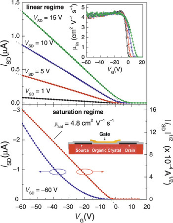
C i is the gate-channel capacitance of a FET per unit area. These equations indicate that correctly functioning OFETs should exhibit a linear I SD(V G) dependence in the linear regime and a linear I SD1/2(V G) dependence in the saturation regime above the threshold voltage, V T. One can correctly extract the charge-carrier mobility from OFETs only provided that these characteristics have an extended linear portion. An example of such textbook behavior is given in Figure 3, where the transconductance characteristics of a single-crystal rubrene OFET with a vacuum-laminated polymer gate dielectric are shown in both regimes.Reference Yi, Chen, Czelen and Podzorov71 These data show all the hallmark features of a truly high-performance OFET, including (1) exceptional linearity of the characteristics in both regimes, as required by the standard FET model (Equations 1 and 2); (2) negligible contact resistance, signified by the fact that all the transconductance curves in Figure 3a scale correctly with V SD, resulting in the same linear mobility value (a plateau in the inset); (3) nearly zero threshold voltage, indicating that the density of deep traps is very low; (4) similar mobility values in the linear and saturation regimes; and (5) negligible hysteresis (V G is swept back and forth in all the measurements in Figure 3).
Linear (top panel) and saturation (bottom panel) regime measurements of rubrene single-crystal organic field-effect transistors (OFETs) made by the vacuum lamination method.Reference Yi, Chen, Czelen and Podzorov71 The devices demonstrate all the features of classical high-performance FETs. In the linear regime, the transconductance I SD(V G) measured at different source-drain voltage (V SD) values (indicated) exhibits remarkable linearity, as predicted by the FET equation (Equation 1). The extraction of linear mobility using this equation results in all the μ(V G) dependences collapsing on the same plateau (the inset). In the saturation regime, taking a square root of the I SD(V G) curve (blue) results in perfectly linear I SD1/2(V G) characteristics (red), as prescribed by the FET equation (Equation 2). The mobilities in the linear and saturation regimes are consistent. The contact resistance, hysteresis, and threshold voltage are negligible. Note: V G, gate voltage; μlin, linear mobility; μsat, saturation mobility; I SD, source-drain current.

Again, linearity of I SD(V G) and I SD1/2(V G) characteristics in the linear and saturation regimes, respectively, is very important in any OFET measurement, including polycrystalline or amorphous transistors, because the equations used for mobility calculations (Equations 1 and 2) are derived under the assumption that mobility is carrier density independent.Reference Sze and Ng74 Therefore, calculation of μ from the slope of transconductance characteristics is justified only if the characteristics are linear. Unfortunately, “mobility” in OFETs is frequently extracted from highly nonlinear transconductance characteristics at the point of maximum slope. In such devices, nonlinearity usually takes the form of an “S”- or “J”-shaped curve with high curvature, leading to erroneous mobility determination. Such characteristics indicate that the devices do not function properly, and reliable extraction of mobility cannot be performed. In each case of a single-crystal or thin-film OFET, linearity of the OFET’s characteristics has to be ensured before calculating the mobility.
Intrinsic versus trap-dominated charge transport regimes in organic single crystals
Due to significantly reduced disorder, the density of deep and shallow trap states in single-crystal OFETs is usually quite low, which allows studies of the intrinsic electronic properties (i.e., the properties not dominated by trapping) in at least a few cases. Indeed, in an operating OFET, gate-induced charge carriers populate both the extended HOMO or lowest unoccupied molecular orbital (LUMO) band states and localized in-gap trap states (created by disorder) that typically take the form of an exponential band tail.Reference Rivnay, Noriega, Northrup, Joseph Kline, Toney and Salleo77, Reference Haas, Stassen, Schuck, Pernstich, Gundlach, Batlogg, Berens and Kirner78 The shallow trap states have energies smaller than ∼kT (relative to the band edge), where k is the Boltzmann constant and T is temperature, and can exchange carriers with the extended band states (i.e., electronic states in the crystal that are spatially delocalized over many lattice constants) through the competing processes of trapping and thermal excitation, thus reducing the effective carrier mobility, μ, according to the multiple trap and release model:Reference Horowitz79
 $$\mu \, = \,\mu _0 \left[ {\tau _{diff} /\left({\tau _{diff} \, + \,\tau _{tr} } \right)} \right],$$
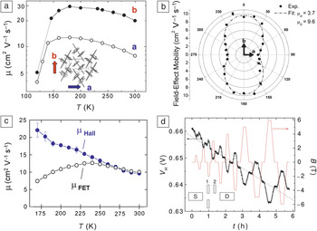
where μ0 is the intrinsic trap-free mobility, τdiff is the average time of carrier diffusion between shallow traps, and τtr is the average carrier retention time on a shallow trap. μ corresponds to the mobility measured in OFETs from the linear transconductance characteristics, and thus this value is affected by shallow traps. In pristine devices with a low density of shallow traps, τdiff >> τtr, and thus according to Equation 3, the measurements yield the intrinsic mobility: μ ∼ μ0. A classic example is pristine rubrene OFETs showing a threshold-less operation,8,9 anisotropic intrinsic mobility (see Reference Reference Gershenson, Podzorov and Morpurgo5), a Hall effect mobility that matches the longitudinal μ,Reference Podzorov, Menard, Rogers, Gershenson, Podzorov, Menard, Rogers and Gershenson29, Reference Takeya, Tsukagoshi, Aoyagi, Takenobu and Iwasa30 and a band-like temperature dependence of mobility.Reference Podzorov, Menard, Borissov, Kiryukhin, Rogers and Gershenson15Figure 4 summarizes some of the fundamental results. In trap-dominated devices, however, τdiff is small due to the high density of shallow traps (τdiff < τtr), and the measured mobility can be significantly smaller than the intrinsic trap-free mobility μ0, which could, in principle, be measured if disorder was eliminated: μ ∼ μ0(τdiff/τtr) < μ0 (Equation 3). Deep traps, on the contrary, have energies greater than kT (relative to the band edge), which makes thermal excitation from these states to the extended band states negligible, thus resulting in a threshold voltage of transistor operation without affecting the mobility.
Some of the fundamental results obtained with single-crystal organic field-effect transistors (OFETs) (the case of rubrene; a and b are the two main crystallographic axes of rubrene). (a) Observation of the intrinsic coherent charge transport in molecular crystals. Non-activated, band-like temperature dependence and anisotropy of longitudinal field-effect mobility measured along a (open symbols) and b (solid symbols) axes (reproduced with permission from Reference Reference Podzorov, Menard, Borissov, Kiryukhin, Rogers and Gershenson15, © 2004 The American Physical Society). The crystal structure of rubrene is shown schematically. (b) Mobility anisotropy. High angular resolution measurements of anisotropy of the field-effect mobility.Reference Sundar, Zaumseil, Podzorov, Menard, Willett, Gershenson and Rogers19, Reference Reese and Bao20 The measurements have been performed using rubrene crystals laminated against PDMS stamps with a high-resolution contact pattern defined by lithography. The fit is a least squares regression of the diagonal mobility tensor with diagonal components μa and μb (reproduced with permission from Reference Reference Reese and Bao20, © 2007 Wiley). (c) Hall effect as evidence of band-like conduction. Temperature dependence of the Hall mobility (μHall, solid symbols) and longitudinal FET mobility (μFET, open symbols), and (d) Hall voltage signal (V H, black) recorded as a function of time (t), as the magnetic field (B, red) is swept back and forth. The black dotted line is a linear fit of the drifting offset voltage that develops on the Hall probes at B = 0 (reproduced with permission from Reference Reference Podzorov, Menard, Rogers, Gershenson, Podzorov, Menard, Rogers and Gershenson29, © 2005 The American Physical Society). A clear change in the Hall effect sign with reversal of the magnetic field direction is observed. Hall-bar/4-probe contact geometry is schematically shown. Note: μ, charge-carrier mobility; T, temperature; μa and μb, hole mobilities measured along a and b crystallographic directions in rubrene, respectively; S, source; D, drain.

The band-like nature of conduction revealed in these electrical measurements has been recently confirmed in ultrafast optical photoconductivity measurementsReference Ostroverkhova, Cooke, Hegmann, Anthony, Podzorov, Gershenson, Jurchescu and Palstra35, Reference Tao, Matsuzaki, Uemura, Yada, Uemura, Takeya, Hasegawa and Okamoto36 and UPS experiments.Reference Nakayama, Machida, Minari, Tsukagoshi, Noguchi and Ishii61, Reference Machida, Nakayama, Duhm, Xin, Funakoshi, Ogawa, Kera, Ueno and Ishii62 In the latter case, the electronic structure of rubrene single crystals was studied by angle resolved UPS, and a clear energy dispersion of the HOMO band with the large dispersion width of 0.4 eV along the well-stacked direction was observed.Reference Nakayama, Machida, Minari, Tsukagoshi, Noguchi and Ishii61, Reference Machida, Nakayama, Duhm, Xin, Funakoshi, Ogawa, Kera, Ueno and Ishii62 The effective mass of holes was estimated to be m* ≈ 0.65·m 0, where m 0 is the bare electron mass. These results confirm that charge transport in rubrene single crystals can be described within the framework of a band model. Interestingly, the effective mass inferred from these measurements is consistent with the unexpectedly light carrier masses (m* ∼ m 0) revealed by infrared optical spectroscopy of the hole accumulation channel in operating rubrene single-crystal OFETs,Reference Li, Podzorov, Sai, Martin, Gershenson, Di Ventra and Basov80 suggesting that there is no significant polaronic effect. Such results contradict the common notion of polaronic nature of charge carriers in molecular crystals, and thus indicate that new theoretical models are necessary to better understand the carrier transport in high-mobility organic semiconductors. The physical aspects of single-crystal OFET operation and conducting interfaces employing organic single crystals are discussed in this issue in the article by Gutiérrez Lezama and Morpurgo.
Theoretical description of charge transport in molecular crystals
The important benefit of single-crystal OFETs is that they allow (or, at least, bring us closer to) experimental access to the intrinsic trap-free mobility μ0 (Equation 3) of the material, which depends only on the molecular structure and crystal packing, thus providing an experimental test bed for modern theories of charge transport in organic semiconductors. Theoretically, charge transport in molecular solids has been considered in the framework of the two limiting cases of a small polaron (localization on each molecular site) and a coherent band-like transport in extended states, with the mean free path being much greater than the lattice constant, λ >> a (delocalized carriers). Indeed, recent transport studies of highly ordered organic crystals seem to suggest that a band-like character of charge transport is realized in a number of systems, such as rubrene and pentacene, where mobility decreases with temperature up to ∼300 K, following a power law: μ ∝ T –α, with α > 0 (see References Reference Gershenson, Podzorov and Morpurgo5 and Reference Bao and Locklin7). However, estimates show that at T > 100 K, the mean free path of the carriers in this transport regime is comparable to the lattice constant of the molecular crystals (λ ∼ a), which contradicts the carrier delocalization assumed in the band model (λ >> a) (see References Reference Gershenson, Podzorov and Morpurgo5 and Reference Bao and Locklin7). This contradiction indicates that the conventional band semiconductor transport model is unable to provide an adequate description of charge transport in organic semiconductors at high temperatures.
A better understanding of the transport mechanisms in molecular crystals has been gained through computational models developed by Brédas and co-workers,Reference Bredas, Beljonne, Coropceanu and Cornil81, Reference Coropceanu, Cornil, da Silva, Olivier, Silbey and Bredas82 showing that realization of either band-like or incoherent hopping regimes (i.e., the regimes of charge motion as a coherent wave or incoherent site-to-site tunneling, respectively) depends on the particular crystal structure and molecular packing which can, in turn, be characterized by two important parameters: the intermolecular transfer integral and electron-phonon coupling. The transfer integral characterizes the strength of the π–π interaction between the adjacent molecules (and thus defines the bandwidth). Two electron-phonon coupling mechanisms, referred to as the Holstein and Peierls models, are usually considered for the description of charge transport.Reference Coropceanu, Cornil, da Silva, Olivier, Silbey and Bredas82, Reference Hannewald and Bobbert83 The Holstein coupling characterizes the change in energy between the charged and neutral states of the molecule due to the geometrical relaxation of the molecule and its surrounding lattice when the charge is present. The Peierls coupling is a result of the sensitivity of the transfer integral to the relative position of the molecules. Therefore, thermal fluctuations lead to significant variations of the transfer integrals, inducing the so-called dynamical disorder of the molecular lattice, which is especially prominent at high temperatures, T > 100 K. Troisi and co-workersReference Troisi and Orlandi84–Reference Cheung and Troisi86 showed that the amplitude of these modulations can be as large as the average transfer integral itself, resulting in the temperature dependence and the magnitude of the carrier mobility to be governed primarily by the fluctuations of the transfer integral rather than the Holstein interaction.Reference Troisi and Orlandi84, Reference Fratini and Ciuchi87 Irrespective of the transport mechanism, an increase of the electronic coupling should lead to an increase in the mobility, while an increase in the Holstein coupling must lead to a decrease of the mobility. The situation is more complex in the case of the Peierls interaction due to its dual nature. On the one hand, as a scattering mechanism, it works toward decreasing the carrier mobility. On the other hand, as a part of the electronic coupling, it works toward increasing the carrier mobility via a phonon-assisted contribution.Reference Sánchez-Carrera, Paramonov, Day, Coropceanu and Brédas88 Critical aspects of the modern theoretical description of charge transport in organic crystals in the framework of the most successful models and computational approaches are described in the article by Coropceanu et al. in this issue.
Exciton dynamics and other optical processes in organic single crystals
High-purity organic molecular crystals are also ideal for optical studies that require minimization of the detrimental interaction of photoexcitations with defects. These materials allow investigation of the complex dynamics of the two basic types of excitons, charge-transfer and Frenkel, in a crystalline molecular environment. The spin state of excitons (singlet and triplet) and their coupling to vibrations result in interesting magneto-optical phenomena in molecular crystals.Reference Ahn, Mueller, Al-Kaysi, Spano, Norton, Belijonne, Bredas and Bardeen44, Reference Muller, Avlasevich, Schoeller, Mullen and Bardeen45 Excitons in these materials exhibit other interesting behavior, including diffusion over large length scales and delayed generation of electron-hole pairsReference Najafov, Biaggio, Podzorov, Calhoun and Gershenson40, Reference Najafov, Lee, Zhou, Feldman and Podzorov41 and exciton fission and fusion.Reference Smith and Michl39, Reference Zimmerman, Zhang and Musgrave89–Reference Chan, Ligges, Jailaubekov, Kaake, Miaja-Avila and Zhu91 The long-range exciton diffusion and exciton fission have particular relevance for the design of organic photovoltaic materials. Bardeen discusses the fundamental excitonic properties of molecular crystals in this issue.
Conclusions
Highly ordered organic molecular crystals represent a powerful platform for basic research in organic electronics due to the low density of defects in these materials. They allow experimental access to the intrinsic material properties, independent of film texture and morphology, thus providing test grounds for modern theories developed to describe charge and energy transport in organic semiconductors. The basic knowledge obtained from studies of organic single-crystal devices also helps to uncover the fundamental performance limits of organic electronics and to formulate new design rules for material synthesis and device fabrication that could enable novel applications.
An important drawback of the current record holder in mobility, rubrene single crystals, in which the reproducible mobilities are in the range of 5–20 cm2 V–1 s–1 (depending on the crystallographic orientation), is that the growth of large-area crystalline films of this material is challenging although not impossible. Indeed, it was demonstrated that crystalline rubrene films can be grown by hot-wall organic molecular beam deposition or by using a special solution processing technique.Reference Käfer and Witte92, Reference Stingelin-Stutzmann, Smits, Wondergem, Tanase, Blom, Smith and de Leeuw93 Nevertheless, one of the important practical goals still to be reached in this field is the development of reproducible high-mobility single-crystalline organic layers grown over large areas on insulating substrates (organic epitaxy).
Broadening the range of molecular crystals in which the intrinsic (trap-free) transport regime is experimentally realized would also be extremely valuable, provided that the trap-free transport is verified by the observation of such signatures of the intrinsic transport as mobility anisotropy and the Hall effect. Microscopic understanding of why some systems exhibit band-like transport, while others do not, is still lacking and is the subject of ongoing experimental and theoretical research. Studies of the intrinsic structure-property relationship in discrete single crystals or homologous series of such crystals with synthetically introduced molecular modifications are very desirable.
An extremely important and continuing task is to understand the origin of disorder and impurities in organic crystals (including those related to exposure to ambient environment) and to develop practical methods of their diagnostics and minimization.
Our understanding of novel electronic effects observed at very high carrier densities (in excess of 1013 cm–2) in electrolyte-gated molecular crystals is still very preliminary at this stage and requires further work.
In terms of optical properties, it is becoming clear that structurally well-ordered molecular crystals exhibit novel excitonic properties, such as delocalization, long-range diffusion, and exciton–exciton interactions. These are important and have to be further investigated because they could be exploited to develop new generations of photovoltaic devices.
Although major progress has been made in the past decade, theory is still unable to quantitatively predict the charge transport characteristics of organic solids. As outlined in a recent review by Troisi and co-workers,Reference Troisi85 the major difficulty is related to our inability to conceptually and computationally account for the effects of the nuclear motion at a multitude of time scales, ranging from extremely short (10–14 s) to extremely long (>10–9s). All of these time scales have an impact on the charge-carrier mobility in organic semiconductors, thus having an impact on a variety of envisioned applications of OFETs.
There are many interesting problems that remain to be experimentally and theoretically addressed in this field. Clearly, the possibility of investigating intrinsic limits of charge and exciton transport in organic semiconductors, without the complications arising from grain boundaries and other defects, will continue to attract researchers to organic single crystals, further expanding our understanding of the fundamental electronic properties of organic semiconductors. An important lesson we draw from the past is that such a quest must be conducted with great care and scientific rigor, with results subjected to independent verification and reproducibility.
Acknowledgments
V.P. is very grateful to W. Hu for his help with co-editing this issue. The author also thanks A.L. Briseno and V. Coropceanu for their input and helpful discussions.