


Introduction
Circularly polarized antennas remain as an active research frontier owing to their superior electromagnetic properties, particularly the combined advantages of multipath interference mitigation and polarization decoupling in transceiver systems. Equal magnitude and  $90^\circ$ phase difference between orthogonal radiating modes are required to achieve circularly polarized (CP) radiation. Feeding network configurations enabling
 $90^\circ$ phase generation constitute a critical implementation approach.
A traditional method is to split the two degenerate modes of a single-feed patch antenna by using perturbation elements such as stubs [Reference Liu, Zhu, Liu, Zhang and Fu1, Reference Jui-Han and Huang2], gaps [Reference Goodwilll, Singh and Kartikeyan3, Reference Dash and Qingsha4], or truncation elements [Reference Kumar, Kanaujia, Khandelwal and Gautam5]. When these two modes work below and above their resonant frequencies, they lead and lag in phase respectively, achieving a  $90^{\circ}$ phase difference. This method is simple and exhibits various performances but is inefficient, often requiring a significant amount of time for full-wave simulation.
Another straightforward approach to generate  $90^\circ$ phase shifts in CP antennas involves integrating quarter-wavelength delay lines into feeding networks [Reference Yan, Jiao, Cheng and Zhang6, Reference Chang and Lin7]. However, dual-band impedance matching networks are typically required prior to the delay lines to align feedline branches with specified port impedances. Moreover, a 3-dB coupler can alternately generate a
 $90^\circ$ phase difference while maintaining equal magnitude [Reference Tong, Xu, Zhang and Yu8–Reference Luo10]. Nevertheless, this design paradigm intrinsically postulates static load impedance profiles, fundamentally misaligned with the frequency-variant impedance characteristics of patch radiators. Dual-band
 $90^\circ$ phase shifters constitute another CP synthesis methodologie [Reference Zuo, Yang and Zhang11–Reference Cao and Guo15]. It can be noted that most designs use
 $90^{\circ}$ phase shifters and Wilkinson power dividers to form a feeding network. This not only increases the complexity of the design, but also achieves performance at the cost of resistor power consumption. Mishra et al. [Reference Mishra, Verma, Yashwanth and Singh16] provides a comprehensive survey of the methods described above.
At last, in Mao et al. [Reference Mao, Gao, Wang, Chu and Yang17] and Li et al. [Reference Li, Su, Yao, Zhang, Lin and Fan18], coupled resonators in dual paths achieve orthogonal polarization amplitude responses, with an additional resonator in one path providing  $90^\circ$ phase shift for CP radiation. However, the coupling design between multiple components increases complexity. Critically, two radiation structures are used to achieve dual frequency, typically requiring an impedance matching network. Zhang and Zhu [Reference Wu, Zhang and Zhu19] and Wu et al. [Reference Wu, Zhang and Zhu20] demonstrated single-band CP operation using tapped-line and parallel coupled-line with detailed phase characteristic analysis.
Traditional dual-band dual-circularly polarized antenna designs face major constraints, including the need for additional impedance matching networks and dedicated phase shifters, which substantially increase design complexity. Consequently, the antenna design requires time-consuming full-wave optimization. Addressing the inherent constraints of conventional dual-band circularly polarized antenna designs constitutes a critical technical challenge. Considering these aspects, the synthesis of integrated coupling structures with SIRs in this paper effectively circumvents the need for dedicated phase shifters and impedance matching networks.
In this paper, a new dual-band dual-CP antenna design is presented based on the dual-band phase characteristics of tapped lines and parallel coupled-line structures. Firstly, coupled resonators are utilized to excite orthogonal radiation modes in dual bands. The feedlines are divided into two paths and the above two coupling methods are selected to provide the required  $90^\circ$ phase difference.
 $\lambda$/2 SIRs are then carefully designed to maintain impedance matching between radiation patch and input port. Finally, a T-junction combines both feeding paths at the output terminal.
In contrast to conventional dual-band dual-CP antennas, the proposed work incorporates impedance matching, equal magnitude excitation, and phase-shifting capabilities within a unified structure. The SIRs are primarily intended as the foundational stage of a second-order Chebyshev filter low-pass filter prototype, their inherent configuration intrinsically provides both impedance matching and phase shift functionalities upon integration. The proposed antenna, supported by a rigorous theoretical framework, enables a systematic implementation process. In second and third sections, the principles and processes of the design are discussed and demonstrated in detail. Next section is on simulation and measurement, and the final section is conclusion.
Dual circularly polarization design principle
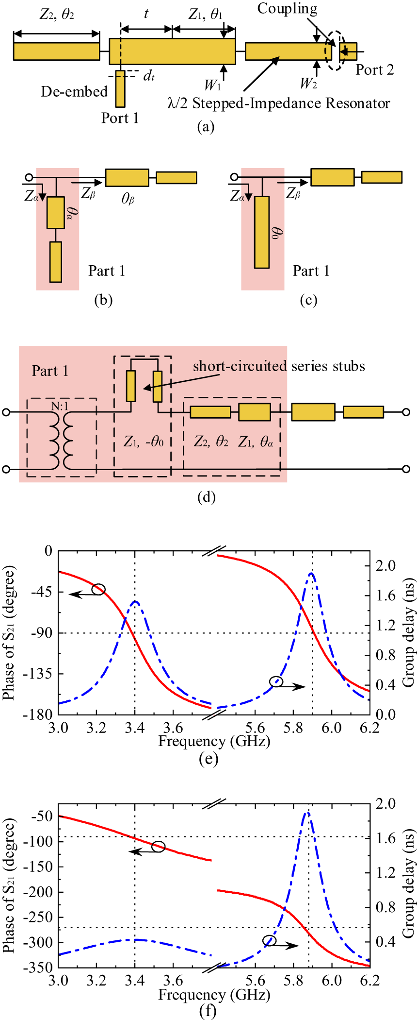
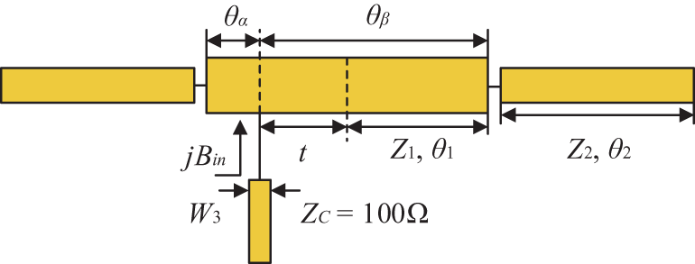
Figure 1(a) depicts the tapped-line coupled structure.  $\lambda$/2 SIRs are directly fed via uniform feeding lines. The feed point is located at distance
 $t$ from the resonator center. To better illustrate the transmission phase characteristics, this structure is modeled using equivalent circuit analysis.
The equivalent can be roughly divided into three steps. Firstly, after de-embedding the feedline, the input impedance measured from the Port1 is divided into two parts with respective impedances  $Z_\alpha$ and
 $Z_\beta$, as illustrated in Fig. 1(b). Based on transmission line theory, the impedance
 $Z_\alpha$ can be derived as (1a).
Geometry, and equivalent circuit of the tapped-line coupling structure. (a) Geometry. (b), (c) Uniform resonator equivalent. (d) Equivalent circuit. (e)  $t = 5.47\,\mathrm{mm}$, Phase and group delay of S21. (f)
 $t = 9.54\,\mathrm{mm}$, Phase and group delay of S21.

 \begin{equation}
Z_{\alpha}=jZ_{1}\frac{R_{z}\tan\theta_{\alpha}\tan\theta_{2}-1}{R_{z}\tan\theta_{2}+\tan\theta_{\alpha}},
\end{equation}
 \begin{equation}
R_{z}=Z_{1}/Z_{2},\ \theta_{\alpha}+\theta_{\beta}=2\theta_{1}.
\end{equation}
Secondly, by applying (2), the  $Z_\alpha$-part is approximated as a uniform-impedance resonator (UIR) with characteristic impedance
 $Z_1$ and electrical length
 $\theta_{0}$, as illustrated in Fig. 1(c). To facilitate subsequent analysis, the UIR section is labeled as Part 1.
 \begin{equation}
Z_{\alpha}=\frac{jZ_{1}}{\tan\theta_{0}},\ \frac{1}{\tan\theta_{0}}=\frac{1-R_{z}\tan\theta_{\alpha}\tan\theta_{2}}{R_{z}\tan\theta_{2}+\tan\theta_{\alpha}}.
\end{equation}
Finally, the ABCD matrix of Part 1 is given by (3).
 \begin{equation}
ABCD=\begin{pmatrix}1 & 0 \\ jY_{1}\tan\theta_{0} & 1\end{pmatrix},
\end{equation}
 \begin{equation}
\begin{aligned}
ABCD=\begin{pmatrix}\cos\theta_{0} & 0 \\0 & \sec\theta_{0}\end{pmatrix}\begin{pmatrix}1 & -jZ_{1}\tan\theta_{0} \\0 & 1\end{pmatrix} \\
\begin{pmatrix}\cos\theta_{0} & jZ_{1}\sin\theta_{0} \\ jY_{1}\sin\theta_{0} & \cos\theta_{0}\end{pmatrix}.
\end{aligned}
\end{equation}
The matrix of Part 1 can be further equivalently expanded into (4), where the first term is equivalent to a transformer with a turns-ratio  $N$ of
 $cos\theta_{0}$, the second term is a short-circuited series stub with electrical length
 $-\theta_{0}$, and the third term is a uniform transmission line with characteristic impedance
 $Z_1$ and electrical length
 $\theta_{0}$, as shown in Fig. 1(d). Meanwhile, by applying (2) again, the third term can be reconfigured in the form of a stepped impedance, which can be modeled as SIRs in conjunction with subsequent parts.
Clearly, we can theoretically predict the transmission phase of this equivalent circuit structure. The first term, the transformer introduces a  $0^\circ$ phase shift when
 $N \gt 0$, and a
 $-180^\circ$ phase shift when
 $N \lt 0$. The second term has almost no effect on the phase shift. The third term,
 $\lambda$/2 SIRs, introduces a
 $-180^\circ$ phase shift at low band and a
 $-360^\circ$ phase shift at upper band.
Furthermore, the equivalent circuit also illustrates the impact of the tapped point position  $t$ on the phase response of the structure. The position of the tapped point
 $t$, electrical length
 $\theta_{1}$ and
 $\theta_{2}$ can be carefully designed to enable the tapped-line coupled SIRs structure to generate distinct phase shifts.
Theoretically, the tapped-line coupled SIRs structure can generally two types of transmission phase situations. By adjusting the equivalent  $\theta_{0} $, the sign of
 $\cos\theta_{0}$ can be altered, enabling the transformer can introduce
 $0^{\circ}$ or
 $-180^{\circ}$. When the equivalent electrical length
 $\theta_{0} \lt 90^\circ$ in both frequency bands, the corresponding phase situation observed at Port 2 for lower and upper frequencies can be expressed as (5a) and (5b).
 \begin{equation}
TPhase_{_{low}}=0^{\circ}-180^{\circ}+90^{\circ}=-90^{\circ},
\end{equation}
 \begin{equation}
TPhase_{_{high}}=0^{\circ}-360^{\circ}+90^{\circ}=-270^{\circ}.
\end{equation}
The entire equivalent circuit structure introduces the transmission phase for the first two terms, and the coupling part of port 2 introduces a phase of  $90^\circ$.
 \begin{equation}
TPhase_{_{low}}=0^{\circ}-180^{\circ}+90^{\circ}=-90^{\circ},
\end{equation}
 \begin{equation}
TPhase_{_{high}}=-180^{\circ}-360^{\circ}+90^{\circ}=-450^{\circ}.
\end{equation}
Similarly, When the equivalent electrical length  $\theta_{0} \lt 90^\circ$ in lower band, and
 $\theta_{0} \gt 90^\circ$ in upper band, the corresponding phase situation for lower and upper frequencies can be expressed as (5c) and (5d).
To validate the above hypothesis, the structure in Fig. 1(a) is simulated, and it is implemented on a substrate with  $\varepsilon_{r} = 2.2$ and thickness of 1 mm. The resonator dimensions are:
 $L_1 = 6.35\,\mathrm{mm}$,
 $L_2 = 9.55\,\mathrm{mm}$,
 $W_1 = 2.86\,\mathrm{mm}$,
 $W_2 = 1.44\,\mathrm{mm}$, and feedline width is 0.86 mm. The resonant frequency is 3.4 GHz/5.9 GHz.
As shown in Fig. 1(e),  $t = 5.47\,\mathrm{mm}$,
 $\theta_{0}=68^\circ/109^\circ$, the low band
 $\cos\theta_{0} \lt 90^\circ$, and the high band
 $\cos\theta_{0} \gt 90^\circ$. Near the dual-band resonance points, the phase exhibits approximately
 $-90^\circ$. These phases are not exactly equal to
 $-90^\circ$, as may be caused by the discontinuity of the SIRs. The group delay and phase exhibit disparities, as the plotted group delay data is derived from
 $S_{11}$ parameters, whereas phase is calculated from
 $S_{21}$ parameters. Figure 1(f),
 $t = 9.54\,\mathrm{mm}$,
 $\theta_{0}=31^\circ/50^\circ$, corresponds to another scenario. These indeed confirm our previous hypothesis.
Obviously, the two situations correspond to same-sense circular polarization and dual circular polarization designs, respectively, revealing further design potential for this structure. And, this paper focuses on the dual CP design.
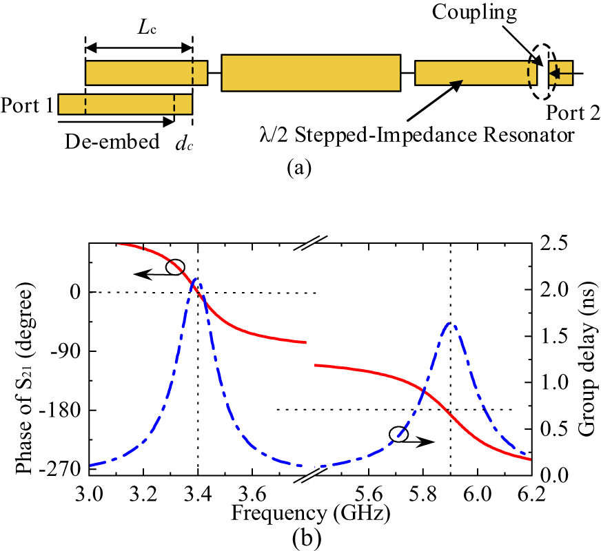
Figure 2(a) depicts the parallel-coupled line structure achieves coupling between the uniform feedline and SIRs through proximity. Analogous to the analysis in [Reference Wu, Zhang and Zhu19], it is theoretically inferred that the parallel-coupled lines introduce  $90^\circ$ phase delay in dual band, and the
 $\lambda$/2 SIRs provides a
 $-180^\circ$ phase at low band and a
 $-360^\circ$ phase at upper band, as derived in (6a) and (6b). The structure in Fig. 2(a) is simulated on the same substrate. As shown in Fig. 2(b), the phase approximates
 $0^\circ$ at the lower band and
 $-180^\circ$ at the upper band demonstrate that the parallel coupled line structure provides a
 $90^\circ$ phase delay in the dual band.
 \begin{equation}
TPhase_{_{low}}=90^{\circ}-180^{\circ}+90^{\circ}=0^{\circ},
\end{equation}
 \begin{equation}
TPhase_{_{high}}=90^{\circ}-360^{\circ}+90^{\circ}=-180^{\circ}.
\end{equation}
Geometry and simulated results of the coupled-line coupling structure: (a) geometry and (b) phase and group delay of S21.

Based on the above analysis, (5a), (5d) and (6a), (6b) can be used in the design of dual band dual circularly polarized antenna.
Antenna structure and SIRs design
Antenna structure
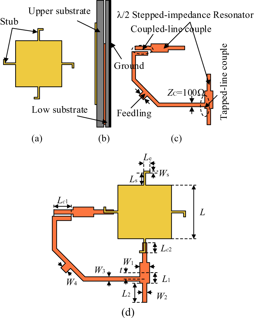
The proposed antenna is illustrated in Fig. 3, the radiating patch achieves dual-band operation by stub-loading techniques that excite both the  $\mathrm{TM}^{01,10}$ and
 $\mathrm{TM}^{03,30}$ modes [Reference Zhang, Zhu, Liu and Wu21]. The addition of stubs decreases the frequency separation among the
 $\mathrm{TM}^{01,10}$ and
 $\mathrm{TM}^{03,30}$ modes, thereby providing design freedom in realizing frequency ratios within a targeted range. Characteristic mode analysis (CMA) is applied to analyze the radiating structure, the external quality factors
 $Q_{e}^{L} = 13$ and
 $Q_{e}^{H}$ = 31 correspond to resonant frequencies of 3.4 and 5.8 GHz, respectively. Two F4B substrates (
 $\varepsilon_{r} = 2.2$) with thicknesses of 4 mm (upper substrate) and 1 mm (lower substrate) are used here.
Geometry of the proposed patch antenna: (a) patch radiator, (b) side view of the whole structure, (c) microstrip feeding network, (d) top view with transparent substrates. ( $L = 20\,\mathrm{mm}$,
 $L_s = 9\,\mathrm{mm}$,
 $W_s = 0.35\,\mathrm{mm}$,
 $L_e = 1.65\,\mathrm{mm}$,
 $W_1 =3.6\,\mathrm{mm}$,
 $L_1 = 6.6\,\mathrm{mm}$,
 $W_2 = 1.44\,\mathrm{mm}$,
 $L_2 = 9.5\,\mathrm{mm}$,
 $t =4.97\,\mathrm{mm}$,
 $L_{c1} = 9\,\mathrm{mm}$,
 $L_{c2} = 8\,\mathrm{mm}$,
 $W_3 = 0.86\,\mathrm{mm}$,
 $W_4 =3\,\mathrm{mm}$ ).

Our design is based on a second-order Chebyshev low-pass filter prototype configuration, which inherently guarantees that all specifications are satisfied. The antenna’s performance is both theoretically predictable and practically achievable within the design framework. The initial topology is established during the preliminary design stage through its inherent parametric definition. Consequently, subsequent minor calibration of the calculated parameters achieves the required performance metrics. This methodology significantly reduces the reliance on extensive iterative simulation during design validation.
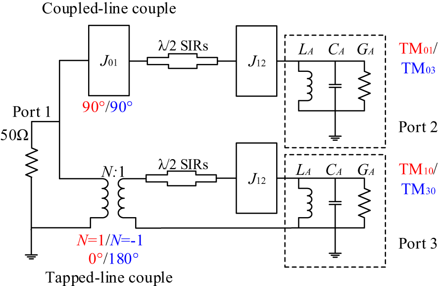
Fig. 4 illustrates the equivalent circuit model of the entire antenna, demonstrating the underlying principles and the implementation methodology employed in the design. The entire antenna is considered as a three-port network. The two orthogonal modes of the two frequency bands of the radiating patch are modeled as parallel GLC ( $\textit{G}_A$,
 $\textit{L}_A$, and
 $\textit{C}_A$) resonant circuits. The proximity couplings between the SIRs and patch radiator are modeled as
 $\textit{J}$ inverters with
 $-90^{\circ}$ phase shift. The detailed analysis of the phase characteristic principles of tapped-line and parallel coupled-line coupling is discussed in “Dual circularly polarization design principle” section. Here, the parallel coupled-line coupling is modeled as a
 $\textit{J}$ inverter with a
 $90^{\circ}$ phase shift, while the tapped-line coupling establishes the phase reference, exhibiting
 $0^{\circ}$ and
 $180^{\circ}$ phase shifts at the low and upper operating bands, respectively.
Simplified circuit model of the proposed dual-band dual-CP patch antenna.

 $J_{01}$ and
 $J_{12}$ are given by the following,
 \begin{equation}
J_{0,1}^{L,H}=\sqrt{\frac{b_{1}^{L,H}FBW^{L,H}}{Z_{0}g_{0}g_{1}}},
\end{equation}
 \begin{equation}
J_{1,2}^{L,H}=FBW^{L,H}\sqrt{\frac{b_{1}^{L,H}b_{2}^{L,H}}{g_{1}g_{2}}},
\end{equation}
 $b_1$ the
 $b_2$ are the slope parameters of SIRs and radiation patch, respectively. Next, the determination of the SIRs and coupling coefficient in the equivalent circuit model are presented in sequence.
SIRs design
Two constraints are used to design SIRs, as illustrated in Fig. 5. Firstly, SIRs are required to resonate at dual bands. The resonance conditions for fundamental and second resonant modes of SIRs are derived as,
 \begin{equation}
R_{z}\tan\theta_{1}\tan\theta_{2}-1=0,R_{z}\tan k\theta_{2}+\tan k\theta_{1}=0.
\end{equation}
Schematic diagram of SIRs design and matching with external impedance

Secondly, two feed lines must be configured to a characteristic impedance of  $100\ \Omega$ when terminated at a
 $50\ \Omega$ port.
 $Z_{C}^{\mathrm{I},\mathrm{II}}$ represent the
 $100 \omega$ impedance to be matched in dual bands. In fact, we have successfully transformed impedance matching requirements into constraints for SIRs, so that the designed SIRs naturally meet the design requirements. The impedance matching condition between feed line and SIRs can be defined as,
 \begin{equation}
Z_{C}^{\mathrm{I},\mathrm{II}}=Q_{e}(\frac{f}{2}\frac{dB}{df})^{-1}|_{f=f_{2},f_{1}},
\end{equation}
where  $B$ is the total resonator’s susceptance seen from the feed line at the tapped point,
 $Q_{e}^{L} = 13$,
 $Q_{e}^{H} = 31$, and
 $Z_{C}$ =
 $100\ \Omega$. According to (1a), (1b), the input admittance looking inward from the tapped point can be derived as (10a). The reactance slope
 $b$ for both resonant modes of the proposed SIRs is defined and derived as (10b). The four constraints correspond to four variables
 $R_z$,
 $\sigma$,
 $\mu$,
 $Z_1$. And
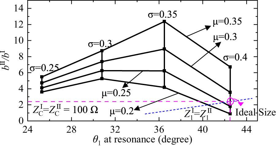
 $\theta_{1}$ is considered as the initial value based on the analysis requirements in Section 2. According to (1b), (8), (9), (10a), (10b), (10c), and the determined values
 $\textit{k}= f_{_2}/f_{_1}$ =1.6,
 $Q_{e}$,
 $Z_{C}$, we can obtain the initial physical dimensions of the SIRs, as shown in Fig. 6.
 \begin{equation}
B=Y_{1}(\frac{R_{z}\tan\theta_{2}+\tan\theta_{\alpha}}{R_{z}\tan\theta_{\alpha}\tan\theta_{2}-1}+\frac{R_{z}\tan\theta_{2}+\tan\theta_{\beta}}{R_{z}\tan\theta_{\beta}\tan\theta_{2}-1}),
\end{equation}
 \begin{equation}
b_1^{L,H}=(\frac{f}{2}\frac{dB}{df})|_{f=f_{2}f_{1}},
\end{equation}
 \begin{equation}
\sigma=\theta_{\alpha}/(\theta_{\alpha}+\theta_{\beta}),\ \mu=\theta_{\alpha}/\theta_{1},
\end{equation}
 \begin{equation}M_{1,2}^{L,H}=\frac{J_{1,2}^{L,H}}{\sqrt{b_{1}^{L,H}b_{2}^{L,H}}},\ \mathrm{FBW}=\frac{g_{2}g_{3}}{Q_{e}}.
\end{equation}
Reactance slope ratio versus ratio of resonant electric length  $\theta_1$ under varied structure parameters.

Coupling coefficient extraction
To determine the theoretical performance of the antenna, we consider the entire antenna structure as a second-order filter. The normalized element values of  $g_{0} = 1$,
 $g_{1} = 0.6292$,
 $g_{2}= 0.9703$,
 $g_{3}= 0.6292$ are derived in [Reference Hong and Lancaster22] for a Chebyshev-type low-pass filter prototype with 0.01-dB ripple. The required coupling coefficients M and the initial bandwidth FBW of the antenna can be calculated, according to the (11), with required
 $M_{12}^{L} = 0.0984$ and
 $M_{12}^{H} = 0.0413$,
 $FBW^{L} = 6\%$,
 $FBW^{H} = 2.5\%$.
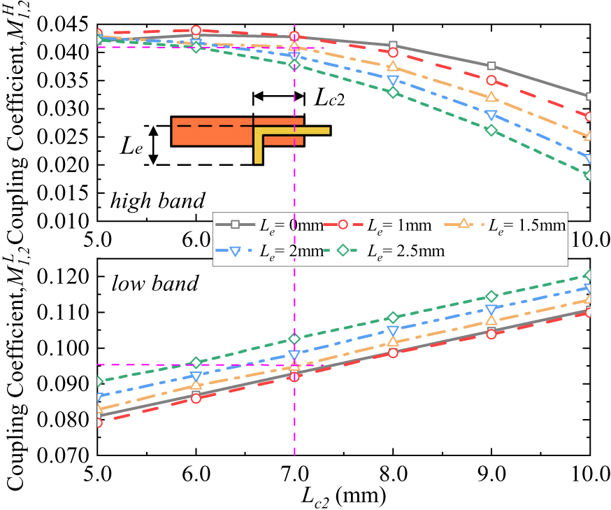
Two design degrees  $L_{c2}$ and
 $L_{e}$ are used to achieve dual-band coupling coefficient requirements. The relationship is shown in Fig. 7, and the size that meets the requirements is obtained.
Coupling coefficient extraction.

Design overview
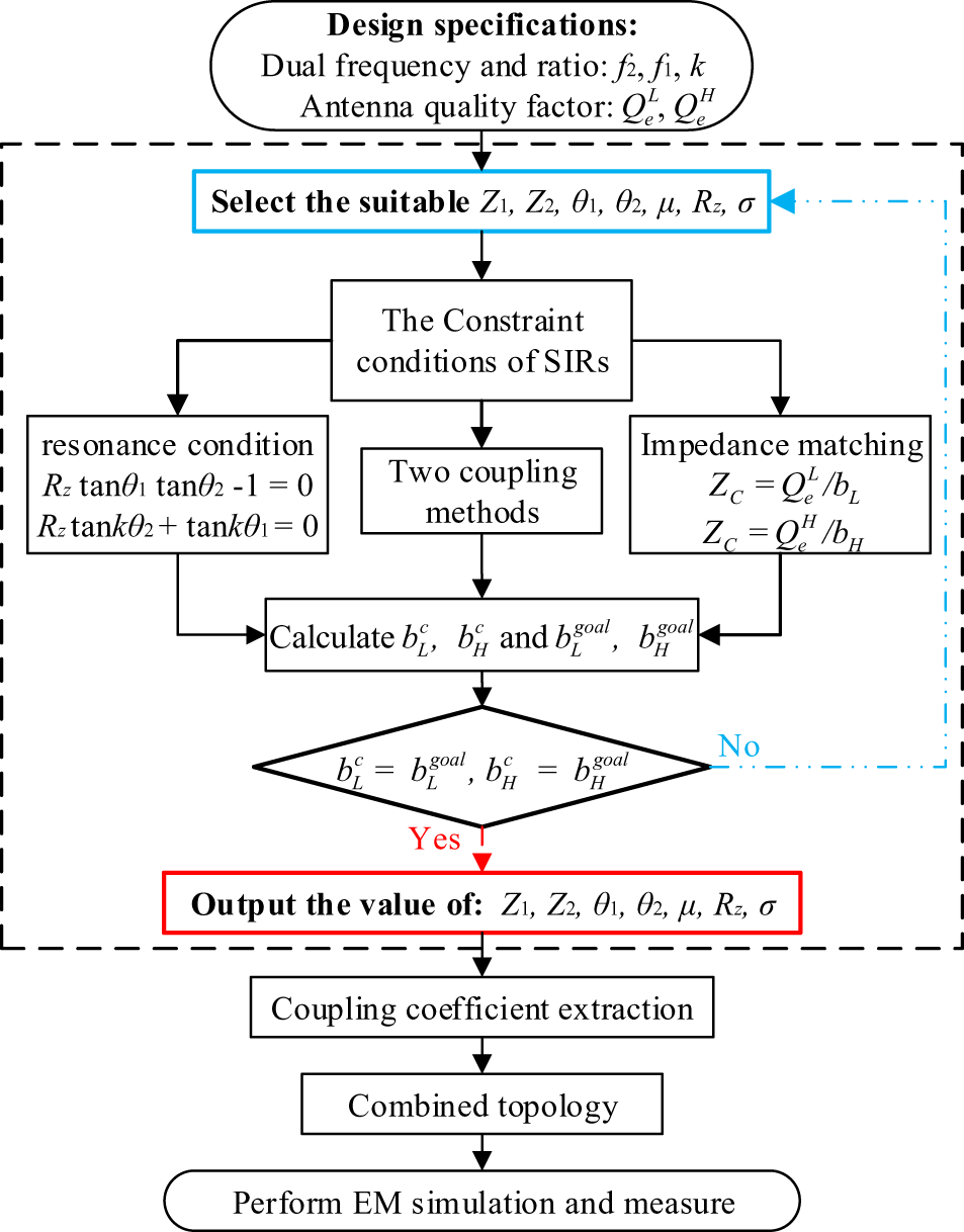
To clarify the design process, the detailed flowchart is illustrated in Fig. 8. The design process can be divided into three steps. Firstly, A single dual-band radiating patch is initially designed, with its operational frequencies ( $f_1$,
 $f_2$) and frequency ratio (
 $k=f_2/f_1$) constituting the primary design constraints for the SIRs. Secondly, the impedance matching requirements dictate additional design constraints for the SIRs. Subject to the dual constraints, the resulting SIRs inherently fulfills the impedance matching requirements while simultaneously exciting orthogonal radiating modes within each operation band of the patch. The two SIRs are fed respectively by a tapped-line coupler and a parallel coupled-line coupler, enabling the realization of a
 $90^{\circ}$ phase shift. a T-junction is used to combine the two paths to the input port. Finally, the coupling coefficient between the SIRs and the radiating patch is calculated, and the AR response exhibits a dual-minima within each operational band. Following the three-step design process, the antenna topology is fully defined. The subsequent stage entails only limited-scope verification simulations and parametric fine-tuning.
Flow chart of the proposed antenna.

Experiment validation and results
The quality factors  $Q_{e}^{L} = 13$ and
 $Q_{e}^{H}$ = 31 correspond to resonant frequencies of 3.4 and 5.8 GHz, respectively. Required coupling coefficients
 $M_{12}^{L} = 0.0984$ and
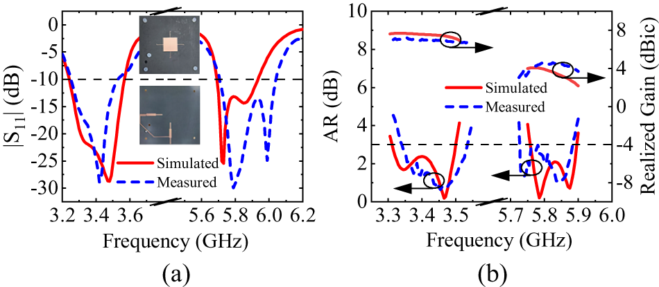
 $M_{12}^{H} = 0.0413$ between antenna and resonators are determined via the proposed methodology. The fabricated CP antenna prototype undergoes experimental characterization. The simulated and measured reflection coefficients, axial ratio (AR), and gain responses are depicted in Fig. 9. Measured impedance bandwidths reach 9.7% (3.24–3.57 GHz) and 4.3% (5.69–5.94 GHz), while 3-dB AR bandwidths attain 5.88% (3.34–3.54 GHz) and 2.67% (5.73–5.88 GHz). Within the AR bandwidth, the measured XPD remains consistently above 15 dB. The measured peak gains in both working bands are 7.15 dBic and 4.59 dBic. The reflection coefficients,
 $|S_{11}|$, of the fabricated patch antenna is measured by an SNA5000X vector network analyzer (VNA), and the farfield of the patch antenna is measured by SATIMO Measurement Systems. As shown in the Fig. 10.
Simulated and measured: (a) reflection coefficients. (b) AR responses and realized gains of the proposed antenna.

Photographs of physical antenna measurement: (a) far-field measurement and (b) S-parameter measurement.

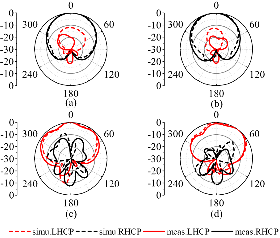
Figure 11(a), (b) shows the simulated surface current distributions at 3.4 GHz and the direction of current on the patch rotates anticlockwise achieving right-hand CP (RHCP) radiation wave. Fig. 11(c), (d) shows the simulated surface current distributions at 5.8 GHz and the direction of current on the patch rotates clockwise achieving left-hand CP (LHCP) radiation wave. Figure 12 illustrates simulated and measured radiation patterns, confirming RHCP/LHCP wave radiation at boresight direction for lower/upper operating frequencies. Close agreement between measured and simulated results validates the proposed design methodology.
Simulated current distributions of the proposed CP antenna at 3.4 and 5.8 GHz: (a)  $t=0^{\circ}$ at 3.4 GHz, (b)
 $t=90^{\circ}$ at 3.4 GHz, (c)
 $t=0^{\circ}$ at 5.8 GHz, (d)
 $t=90^{\circ}$ at 5.8 GHz.

Simulated and measured radiation patterns of the proposed antenna: (a) xoz-plane, 3.4 GHz, (b) yoz-plane, 3.4 GHz, (c) xoz-plane, 5.8 GHz, (d) yoz-plane, 5.8 GHz.

Table 1 presents a comparison between the proposed antenna with other dual-band dual CP patch antennas. Although the proposed antenna does not have the smallest profile, it offers a well-balanced performance throughout all its working bands, and no additional matching network is required. The high gain in [Reference Wu, Zhang, Zhu, Wang, Zhang and Guo24, Reference Zhu, Xu, Ren, Wang, Huang and Wu25], and [Reference Zhang, Zhu, Liu and Wu21] is primarily originates primarily from the array configuration. Although [Reference Wang, Chen, Wang and Wu26] provides a wider AR bandwidth, it is mismatched with its own working bandwidth. And the design of phase shifter and dual band Wilkinson power divider significantly increases the complexity of the antenna.
Comparisons with other dual band dual cp patch antennas

 $\lambda_0$: Corresponding to the center operation frequency of the higher band.
Conclusion
A dual-band dual CP antenna design methodology utilizing tapped-line and coupled-line coupling SIRs is proposed in this letter. Dual CP operation is achieved by the phase characteristics of tapped-line coupled resonators. The proposed design incorporates the dual-band resonance requirements and  $50\omega$ port matching specifications into SIRs geometric parameters, thereby simplifying the feeding networks. A prototype fabricated through this approach demonstrates measured impedance bandwidths of 9.7% (3.24–3.57 GHz) and 4.3% (5.69–5.94 GHz), with 3-dB axial ratio bandwidths reaching 5.88% and 2.67% respectively. Close agreement between simulated and measured confirming the methodology’s effectiveness.
The proposed design demonstrates inherent simplicity alongside complete analytical verification, delivering practical solutions for satellite communication systems and autonomous vehicles. In future research, the SIRs can be reconfigured into bent geometries and integrated to realize a compact dual-frequency radiating structure for further miniaturization, enabling investigations including modular array formation.
Competing interests
The authors report no conflict of interest.

Qiong-Sen Wu received the B.Eng. degree in Information Engineering and the M.Eng. degree in Electromagnetism and Microwave Engineering from South China University of Technology, Guangzhou, China, in 2011 and 2014, respectively, and the Ph.D. degree in electrical and computer engineering from the University of Macau, Macau, SAR, China, in 2018. He joined the Antenna and Electromagnetic-Wave Laboratory in University of Macau, Macau, SAR, China, as a research fellow in May 2018. He is currently an associate professor with the School of Integrated Circuits, Guangdong University of Technology. His current research interests include microwave circuits and planar antennas with improved functionalities.

Hao Zhu received the B.Eng. degree in Electronic Science and Technology from the Guangdong University of Technology, Guangzhou, China in 2023. He is currently pursuing his M.S. degree in Microelectronics and Solid-State Electronics at Guangdong University of Technology.