I. INTRODUCTION
Thermoelectricity has seen a renewed emphasis, since the early 2000s due to the development of new materials with improved performances. This growing interest is reinforced by the fact that the solid-state thermoelectric (TE) devices can convert waste heat from sources, such as power plants, factories, motor vehicles, and computers, to electric power using the Seebeck effect and then contribute to a sustainable development. The TE devices can be utilized to various applications, such as infrared sensor, microcalorimeter, flow meter, vacuum sensor, accelerometer, optoelectronics cooling, and refrigeration/cryosurgery instrument. Among the synthesis methods of TE materials, electrodeposition appears as a cost-effective approach in comparison with dry conventional film synthesis techniques. Especially for the fabrication of microelectromechanical systems, electroplating provides an excellent synthetic approach, which combines the advantages of comparatively simple equipment and processing conditions with high-growth rates and well controlled material properties. It is a useful tool for patterning small structures, minimizing the waste material due to the selective deposition. Moreover, the bismuth telluride-based compounds, which are the best TE materials at room temperature until now, can be directly synthesized by cathodic reaction. Consequently, since the first report of the electrodeposition of thin Bi2Te3 films from acidic baths in 1993,Reference Takahashi, Oda, Ogino and Furuta1 the number of publications on this topic has been steadily increasing, with around 30–40 yearly contributions being reached in 2009. The majority of the papers have been devoted to the study of the associated electrochemical systems without any characterization of TE properties. This feature is not surprising and is due to the difficulty of measuring active layers on electrically conductive substrates and particularly to the complexity of the electrochemical systems. The advances in the field were previously described in two review papers by Xiao et al. in 2008Reference Xiao, Hangarter, Yoo, Rheem, Lee and Myung2 and Boulanger in 2010.Reference Boulanger3
The first objective of this paper is to update the literature data concerning the electrodeposition of TE V–VI films, with more than 40 novel, related papers. The different features of the electroplating processes will be presented successively for the n-type Bi2(Te, Se)3 and the p-type (Bi, Sb)2Te3 films. Our editorial choice is to give a review on the electrochemical synthesis of V–VI films, and then we discarded the works devoted exclusively to the nanowires. One reason for this choice is that the synthesis of nanowires implies specific developments different from the films.
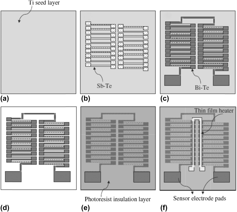
As an emerging technology, the interest of electrodeposition of TE compounds has to be demonstrated by the fabrication and the characterization of specific devices (Fig. 1). Thus, the second objective of this work is to establish, as far as possible, for the first time, an exhaustive state-of-the-art on the published fabrication processes of miniaturized TE devices based on electroplated legs. This will constitute the second part of this paper.
TE microdevice based on electroplated legs.

II. ELECTROCHEMICAL DEPOSITION OF n-TYPE V–VI FILM
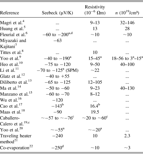
In this section, the main results from the literature are presented along the key steps of the electrodeposition method. While the selection of included papers is by necessity, somewhat arbitrary, the overview should cover most of the relevant developments in the field. The obtained TE properties are given in Table I to gain a general impression of the achieved results. The more specific results and contributions will, however, be discussed in more detail within the next sections. The section will be finished by a brief description about the synthesis of the ternary compound Bi2Te2.7Se0.3, which is rarely observed in the literature data.
Overview of TE properties for selected publications on Bi2Te3 film electrodeposition, comparison with the TE properties of Bi2Te3 fabricated from alternative synthesis methods. Apart from some exceptions, all the measurements were performed parallel to the surface (in plane) and then perpendicular to the film growth direction.
SPM, done by Seebeck Probe Microsope.
a Indicates values obtained for annealed material.
b (00L)-oriented thin films.
c Measured at 50 °C.
d Measured across the sample thickness.
A. Electrolyte
The mechanism for the electrodeposition of Bi2Te3 was thoroughly investigated by Martin-Gonzalez et al.Reference Martin-Gonzalez, Prieto, Gronsky, Sands and Stacy23 The reaction can be considered as the reduction of TeIV species in the presence of Bi3+ cations according to
 $${\rm{2B}}{{\rm{i}}^{{\rm{3}} + }} + {\rm{3HTeO}}_{\rm{2}}^ + + {\rm{9}}{{\rm{H}}^ + } + {\rm{18}}{{\rm{e}}^ - } \to {\rm{B}}{{\rm{i}}_{\rm{2}}}{\rm{T}}{{\rm{e}}_{\rm{3}}} + {\rm{6}}{{\rm{H}}_{\rm{2}}}{\rm{O}}\quad {\rm{.}}$$
Based on a calculated Pourbaix diagram, it is necessary to work in strong acidic medium to ensure the stability of the ionic species in the solution. Recently, one group has tested the synthesis in alkaline solution to avoid the hydrogen evolution in presence of Nitrilotriacetic acid [N(CH2CO2H)3], with the purpose of increasing the solubility of the bismuth cation in such basic solution.Reference Suzuki, Chen and Fuwa24
The first successful electrodeposition of Bi2Te3 from an aqueous, acidic solution based on HNO3 with a pH value of ∼1 was reported in 1993 by Takahashi et al.Reference Takahashi, Oda, Ogino and Furuta1 The deposition was carried out at room temperature under potentiostatic conditions, and nearly stoichiometric material was achieved, as verified by both x-ray diffraction (XRD) and inductively coupled plasma atomic emission spectroscopy measurements. While the electrolyte used in this work had a somewhat low concentration in HNO3, the vast majority of all published works, since this first paper, are based on very similar electrolytes with 1 M HNO3 being the most commonly encountered acid concentration. Generally, a higher concentration of source materials in the electrolyte allows higher deposition rates, and the solubility of Bi is high enough to be unproblematic as opposite to telluride. In nitric acid-based electrolytes, the solubility of Te is one of the main limitations in the electrolyte fabrication and optimization,Reference Martin-Gonzalez, Prieto, Gronsky, Sands and Stacy23 with the highest reported content of 50 mM Te-ions in a 1 M HNO3 solution.Reference Magri, Boulanger and Lecuire4 The most commonly encountered base values are either 10 or 20 mM Te. One notable exception is the work of Glatz et al.,Reference Glatz, Durrer, Schwyter and Hierold12 who used a higher HNO3 concentration of 2 M to increase the solubility of Te in the solution. The use of other acidic media is possible, e.g., as shown by Heo et al.,Reference Heo, Hagiwara, Ichino and Okido10 who used H2SO4, but remains an exception.
Nonaqueous solvents with higher metallic salts solubility beneficial for high deposition rates were tested like molecular organic solvents (dimethylsulfoxide,Reference Nguyen, Su, Wang, Vullers, Vereecken and Fransaer25 ethylene glycol,Reference Wu, Nguyen, Vullers, Vereecken, Binnemans and Fransaer16,Reference Jung and Ko26,Reference Nguyen, Wu, Su, Vullers, Vereecken and Fransaer27 or ionic liquids).Reference Golgovici, Cojocaru, Anicai and Visan28–Reference Szymczak, Legeai, Michel, Diliberto, Stein and Boulanger31 However, these alternative electrolytes imply either an unsatisfying morphology or a complex electrochemical reactivity.
The ratio of Bi:Te in the electrolyte can, in combination with the deposition current or potential, be used to control the composition of the deposited material. In agreement with the case of a codeposition mechanism (not really representative of the phenomenon in our case), a higher ratio of Bi:Te in the electrolyte should lead to a higher ratio of Bi:Te in the deposited film. The actual “optimal” ratio depends on the precise deposition conditions, as well as the overall electrolyte concentration, and no general consensus is found in the literature (see e.g., Refs. Reference Takahashi, Oda, Ogino and Furuta1,Reference Heo, Hagiwara, Ichino and Okido10, and Reference Michel, Diliberto, Boulanger, Stein and Lecuire32). However, the applied Bi:Te ratio is typically on the order of 1:1, with common variations ranging between 2:1 (Ref. Reference Miyazaki and Kajitani7) and 3:4.Reference Manzano, Rojas, Decepida, Abad, Feliz, Caballero-Calero, Borca-Tasciuc and Martin-Gonzalez15 From comparative measurements of diffusion coefficients of Bismuth and Tellurium cations in nitric acid, Schoenleber et al.Reference Schoenleber, Stein and Boulanger33 have demonstrated that the used experimental ratios in the literature are equal or superior to a predicted value of 0.74. This theoretical ratio was based on the assumption that the cathodic deposition reaction is governed exclusively by diffusion mass transport.
To further improve the quality and the morphology of the films, additives, such as surfactants and optical brighteners, are widely used in the electroplating baths. However, concerning the electrodeposition of bismuth telluride, the effect of only one surfactant Sodium Lignosulfonate was recently reported by Naylor et al.Reference Naylor, Koukharenko, Nandhakumar and White34 and later by Caballero-Calero et al.Reference Caballero-Calero, Díaz-Chao, Abad, Manzano, Ynsa, Romero, Rojo and Martín-González19 Thus as-deposited films were obtained with better crystalline quality and improved Seebeck coefficient.Reference Caballero-Calero, Díaz-Chao, Abad, Manzano, Ynsa, Romero, Rojo and Martín-González19
B. Substrate
The choice of substrate is mostly based on the necessary chemical stability in the acidic electrolytes. Typically applied materials are thin sputtered or evaporated layers of gold, platinum, titanium, and nickel on glass slides or oxidized silicon chips, as well as polished metal substrates, e.g., titanium or stainless steel sheets. A particularly strong influence of the substrate material on the deposited films is not mentioned in the literature, with the exception of the substitution reaction between nickel substrates and bismuth and tellurium cations in acidic medium as mentioned by Heo et al.Reference Heo, Hagiwara, Ichino and Okido10 This chemical reactivity was used by Scidone et al., demonstrating that the electroless deposition of a Bi2Te3 film can be obtained from that of Nickel.Reference Scidone, Diliberto, Stein, Boulanger and Lecuire35 Later, a similar approach was used by Chang, with the use of cobalt and iron as the sacrificial metal thin films. Strong dependences were observed between the bismuth and telluride cation concentrations in the electrolyte and the atomic composition and the morphology of the synthesized film.
Otherwise, metallic materials like Pt, Au, or stainless steel can be used as seed layer or substrate. If a removal of the deposited film from the substrate is desired, stainless steel has the advantage of a very low adhesion between film and substrate. This allows performing a lift-off of the deposited material for further characterization.Reference Ma, Ahlberg, Sun, Iversen and Palmqvist14,Reference Schumacher, Reinsberg, Rostek, Akinsinde, Baessler, Zastrow, Rampelberg, Woias, Detavernier, Broekaert, Bachmann and Nielsch36 Since there is a lattice mismatch between a metallic substrate and the deposited film, Cao et al. have tried to reduce it by the use of a 40-nm bismuth telluride epitaxial seed layer deposited by molecular beam epitaxy on silicon.Reference Cao, Zeng, Liu, Zhang, Shen, Wang, Gan, Wu and Hu17 As a result, they have obtained (00L)-oriented Bi2Te3 thin films with low surface roughness and uniform structure consistent with the seed layer. Consequently, a significant improvement of the power factor by 45% was observed.
C. Deposition modes
The cathodic deposition of bismuth telluride can be performed under fixed applied current i.e., galvanostatic mode, under fixed applied potential i.e., potentiostatic mode, pulse potentiostatic or pulse galvanostatic mode. Whatever the investigated growth mode, the results show that the crystalline quality, the morphology, and the compositions of the depositions are highly dependent of the values of the growth parameters (applied potential E or current i). Thus, the electrochemical systems have to be analyzed through the study of the associated cyclic voltammetry curves. As an example with relevance to this work, the paper from Martin-Gonzalez et al. gives a deep analysis of the complex electrochemical reactivity of a Bi–Te solution.Reference Martin-Gonzalez, Prieto, Gronsky, Sands and Stacy23 The information obtained from the electrochemical investigation of an electrolyte system can be used to identify the optimum deposition conditions (E, i) for the targeted material.
Most of the earlier work on Bi2Te3 was conducted under either galvanostatic or potentiostatic conditions. For both cases, the desired stoichiometry and dense morphology of the deposited material can be achieved, and the results are generally quite similar. One comparative study by Michel et al. found that galvanostatic deposition leads to a more pronounced preferred orientation than potentiostatic conditionsReference Michel, Diliberto, Boulanger, Stein and Lecuire32 but yielded otherwise very similar materials. The reported achieved morphologies and accessible compositional range for the investigated publications indicate no significant advantage of either of the static deposition methods. The influence of a pulsed, current controlled deposition was investigated by Richoux et al.,Reference Richoux, Diliberto, Boulanger and Lecuire37 and it was found that a pulsed deposition leads to better morphology and smoother films. The influence of the pulse parameters, i.e., on- and off-time, as well as applied current density, on the nucleation mechanism, morphology, and crystallinity was studied in detail. A novel, mixed pulsed deposition method was introduced by Glatz et al.Reference Glatz, Durrer, Schwyter and Hierold12 and incorporates a potential controlled deposition pulse and a current controlled resting pulse. By using this method, homogenous, high-quality films with constant composition and thickness of up to 800 µm were achieved. Later, a similar pulsed procedure was developed in the group of Martin-Gonzalez, leading to the synthesis of electroplated films exhibiting outstanding crystalline and TE properties.Reference Manzano, Rojas, Decepida, Abad, Feliz, Caballero-Calero, Borca-Tasciuc and Martin-Gonzalez15 An alternative pulsed, potential-controlled deposition was applied by Ma et al.Reference Ma, Ahlberg, Sun, Iversen and Palmqvist14 and compared to results obtained under potentiostatic conditions. The results indicate that the pulsed samples had a less pronounced preferential orientation and allowed better control of the morphology through changing the pulse parameters. The typical on-pulse duration is on the order of 10–100 ms, with relaxation times usually between 50 and 1000 ms. The applied current density or deposition potential is then adjusted accordingly to achieve the desired material composition. As the range of successfully applied parameters is rather large, the optimized recipe is difficult to be targeted. Rather, the protocol needs to be optimized in accordance with the initially set boundary conditions.Reference Wen, Corderman, Seker, Zhang, Denault and Blohm38–Reference Liu and Li41 Overall, pulsed methods can offer some advantages over static methods, e.g., improved morphology and composition control. The larger amount of variable parameters is also an essential benefit, as they allow a more precise control over the deposition process.
D. Deposited material
The deposited films are commonly characterized with respect to their composition, their microscopic morphology, and their crystalline structure and orientation. For actual applications in TE generators, the synthesized film should be smooth, crystalline, and of the correct composition. A homogeneous deposition over the full area is also desired.
1. Composition
As mentioned before, the composition of the deposited material can be controlled through the applied current density or deposition potential. Higher current densities or more negative potentials lead to a decrease in Te content in the deposit, a relation, which has been well established in various publications. Examples for this relationship can be found in virtually every publication mentioned, see e.g., Tittes et al. for galvanostatic conditionsReference Tittes, Bund, Plieth, Bentien, Paschen, Plötner, Gräfe and Fischer8 and Michel et al. for potentiostatic conditions.Reference Michel, Diliberto, Boulanger, Stein and Lecuire32 Achieving the stoichiometric material composition can be considered to be standard procedure, with the only requirement of having an appropriate electrolyte.
2. Morphology
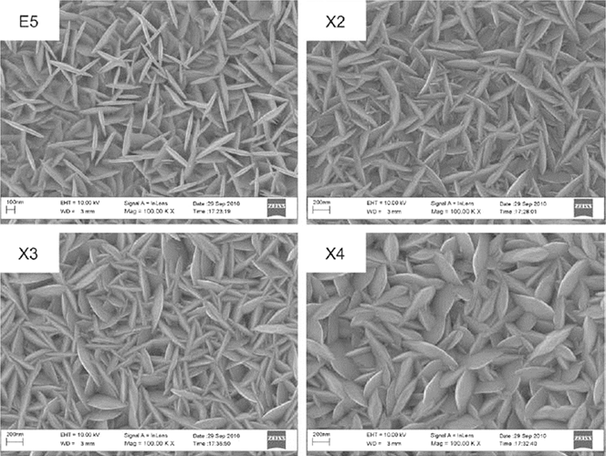
The most frequently encountered morphology for stoichiometric Bi2Te3 is commonly described as needle-like and occurs for both current as well as potential-controlled deposition methods. Other morphologies can be achieved, e.g., granular or dendritic structures,Reference Naylor, Koukharenko, Nandhakumar and White34 but are typically related to either incorrect composition or unreasonably high-growth rates.Reference Michel, Diliberto, Boulanger, Stein and Lecuire32,Reference Wen, Corderman, Seker, Zhang, Denault and Blohm38 Exemplary images for well-formed Bi2Te3 films with the needle like structure, deposited by Ma et al.,Reference Ma, Ahlberg, Sun, Iversen and Palmqvist42 are shown in Fig. 2.
Needle-like surface morphology of electroplated Bi2Te3 films (images taken from Ref. Reference Ma, Ahlberg, Sun, Iversen and Palmqvist42 reproduced by permission of The Electrochemical Society).
3. Thickness
The deposited material thickness varies greatly, with reported values between 100 nm and 800 µm, which are likely due to the different foci of the individual research. For integration into TE generators, a minimum thickness of some tens of microns is required, with higher values being beneficial.Reference Lim, Snyder, Huang, Hennan, Ryan and Fleurial43,Reference Glatz, Schwyter, Durrer and Hierold44 Thick films have been achieved under both potentiostatic and galvanostatic conditions, as reported by Li et al.,Reference Li, Toprak, Soliman, Zhou, Muhammed, Platzek and Muller11 as well as by applying a pulsed deposition method, as reported by Glatz et al.Reference Glatz, Durrer, Schwyter and Hierold12 Therefore, while maybe not necessarily state-of-the-art, the deposition of thick films of Bi2Te3 has been proven to be feasible. An original approach was proposed by Maas et al. with the use of a soluble anode made of bismuth telluride.Reference Maas, Diliberto, de Vaulx, Azzouz and Boulanger18 Thus, dense and homogenous films up to 400 µm were obtained with low-internal stress.
4. Crystallinity
XRD experiments conducted on the deposited films universally confirm the existence of a Bi2Te3 phase, proving that the deposition process leads to at least partially crystallized materials. Most reports also indicate a preferential (110) orientation of the deposited material, as long as it is close to the correct stoichiometry. The crystallization process was studied in detail by Chaouni et al.,Reference Chaouni, Bessieres, Modaressi and Heizmann45 who investigated the orientation of the films as a function of substrate, material composition, and deposition thickness. The investigation revealed that various textures are possible for small growth thicknesses (<10 µm), which are dependent on both stoichiometry and substrate material. However, for films with a thickness of >10 µm, the (110) preferred orientation always appeared, regardless of the initial conditions. This effect is attributed to the higher in-plane electrical conductivity of the highly anisotropic Bi2Te3 crystallites. Similar results were obtained by Richoux et al.Reference Richoux, Diliberto, Boulanger and Lecuire37 in a study investigating the details of the nucleation mechanism for pulsed deposition methods. Additionally, they concluded that pulsed methods lead to smaller aggregates and, therefore, films with decreased roughness. Additionally, the effect of the pH, in the 1–3.5 range, on the structural properties of the material was investigated by Suresh et al.Reference Suresh, Chatterjee, Sharma, Ganguly, Kargupta and Banerjee46 Their results show that an increase in the pH of the solution results in a decrease in the grain size and dislocation density.
E. TE properties
1. Characterization methods
The electrical characterization of electroplated films is complicated by the unavoidable existence of the electrically conductive seed layer underneath the deposited material. The three main approaches to circumvent this problem, which are proposed in the literature, are to remove the deposited layer from the substrate and seed layer, to extract the properties of the deposited layer from the combined measurement or finally to use a thin seed layer composed of the same material as the deposited one.
Removing the deposited material from the seed layer was already proposed by Takahashi et al. in 1994,Reference Takahashi, Katou, Nagata and Furuta47,Reference Takahashi, Kojima, Sato, Ohnisi, Nishiwaki, Wakita, Miyuki, Ikeda and Muramatsu48 who used an epoxy resin to transfer the film onto a glass plate. Similar processes were described in detail by Heo et al.Reference Heo, Hagiwara, Ichino and Okido10 and Ma et al.Reference Ma, Ahlberg, Sun, Iversen and Palmqvist14 The deposited material can then be characterized with standard metrology equipment. A potential disadvantage of this method is that the films can be damaged by the mechanical stress applied during the peeling process. Nonetheless, this method is probably the most commonly applied approach in the literature.
Calculating the film properties based on the measured properties of the seed layer and the measurement of the combined properties was proposed by e.g., Nguyen et al.Reference Nguyen, Su, Wang, Vullers, Vereecken and Fransaer49 and Deb et al.Reference Deb, Isoda, Caballero-Calero, Diaz-Chao, Martin-Gonzalez and Shinohara50 While this method is convenient, it requires an additional measurement of the seed layer properties and is reliant on several simplified assumptions. An experimental investigation of this approach was conducted by Rostek et al.Reference Rostek, Kottmeier, Kratschmer, Blackburn, Goldschmidtböing, Kröner and Woias51 for Bi2Te3 layers on Platinum seed layers with varying thickness for the individual layers. It was concluded that reasonable results with accuracy of better than ∼15% can be achieved for the measurement of the electrical resistance and the carrier concentration, as long as the deposited film thickness is significantly larger than the seed layer thickness (ratio of >50). The determination of the Seebeck coefficient was also possible, however, due to the influence of the thermal properties of the substrate material, is somewhat less accurate, and requires a higher thickness of the TE material (ratio of >125).
Using a seed layer of the same material as the deposited one was proposed by Yoo et al.,Reference Yoo, Huang, Lim, Herman, Ryan, Fleurial and Myung9 who used a seed layer of sputtered Bi2Te3 for the experiments. The measurements of the film can then also be conducted with standard metrology. However, the method relies on the assumption that both layers have similar properties, which might not necessarily be the case. Each of these three methods can be used to obtain the TE properties of electroplated materials. Removing the deposited material from the substrate, if carefully conducted, is, however, probably both the most used as well as the most reliable method.
2. Transport properties
An overview of the obtained TE properties of electrodeposited Bi2Te3 is given in Table I. It is obvious that not every publication contains a full TE characterization of the synthesized material. This is presumably partly due to the different foci of some of these works and partly due to the described difficulties in obtaining these measurements. The most frequently reported value is the Seebeck coefficient, as it represents the most important TE property. This is followed by the electrical resistivity, and finally the carrier concentration, which is only reported in a minority of publications.
3. Seebeck coefficient
The Seebeck coefficients obtained for electroplated materials are typically on the order −40 to −80 µV/K, with maximum reported values around −125 µV/K (e.g., Refs. Reference Heo, Hagiwara, Ichino and Okido10, Reference Diliberto, Richoux, Stein and Boulanger13, and Reference Wu, Nguyen, Vullers, Vereecken, Binnemans and Fransaer16). The majority of publications report that only n-type material is obtained through the electroplating process, regardless of the stoichiometry of the deposited material.Reference Tittes, Bund, Plieth, Bentien, Paschen, Plötner, Gräfe and Fischer8 This is in direct contradiction to the well-established results achieved on materials prepared from melts,Reference Scherrer and Scherrer21 indicating that Te-deficient material should exhibit p-type conductivity. This dominant n-type doping in electroplated materials strongly indicates a different, or possibly additional, doping mechanisms than the antistructure disorder typically associated with Bi2Te3. This effect is discussed e.g., by Diliberto et al. and Ma et al.,Reference Diliberto, Richoux, Stein and Boulanger13,Reference Ma, Ahlberg, Sun, Iversen and Palmqvist14 however, to date no full explanation is available in the literature. While some reports include the fabrication of p-type material,Reference Miyazaki and Kajitani7,Reference Glatz, Durrer, Schwyter and Hierold12,Reference Jung and Ko26,Reference Nguyen, Wu, Su, Vullers, Vereecken and Fransaer27 they remain the exception rather than the rule.
4. Carrier concentration
The comparatively low values for the Seebeck coefficient are related to the high-carrier concentration associated with electroplated materials, which are typically on the order of 1020 to 1021 1/cm³ (Table I). These values are about one order of magnitude higher than the ones obtained for melted material and are responsible for the comparatively overall low TE quality. In combination with the predominantly n-type Seebeck coefficient, the high carrier concentration indicates an additional doping mechanism, which might be related to the high density of grain boundaries in electrochemically deposited materials.Reference Ma, Ahlberg, Sun, Iversen and Palmqvist14
5. Electrical resistivity
The reported values for the electrical resistivity of near-stoichiometric materials are typically around 8–15 µΩ∙m, with worst-case values around 100 µΩ∙m. While these values are comparable to optimized materials, they are mostly related to the high-carrier concentration. The mobility of electroplated films is correspondingly rather low, with typical values around 5–20 cm²/Vs.Reference Magri, Boulanger and Lecuire4,Reference Huang, Wang and Murphy5,Reference Ma, Ahlberg, Sun, Iversen and Palmqvist14,Reference Fleurial, Snyder, Herman, Giauque, Phillips, Ryan, Shakkottai, Kolawa and Nicolet52 These values are about one order of magnitude lower than the ones obtained for optimized materialReference Scherrer and Scherrer21 and possibly also caused by the high density of grain boundaries.
An overview of the TE properties of electroplated materials in comparison to state-of-the-art, optimized materials, fabricated by a thermal bulk synthesis method and by coevaporation is given in Table I.
F. Postannealing treatment
One possible approach to improving the TE properties of the electroplated materials is a postdeposition annealing treatment. This can potentially improve the crystallinity of the materials, thereby increase the mobility, and reduce the defect density. A potential challenge during the annealing treatment is the possible evaporation of tellurium, which is due to its comparatively high vapor pressure.
An annealing treatment in inert or reducing atmosphere, reported by Fleurial et al.Reference Fleurial, Borshchevsky, Ryan, Phillips, Snyder, Caillat, Kolawa, Herman, Mueller and Nicolet6 and Yoo et al.,Reference Yoo, Huang, Lim, Herman, Ryan, Fleurial and Myung9 leads to a pronounced increase of the carrier mobility from 20 to 60 cm²/Vs and a decrease in carrier concentration to values in the 1019 1/cm³ range. The Seebeck coefficients increased accordingly to values of up to −200 µV/K. Similar results have been reported by Li et al.Reference Li, Toprak, Soliman, Zhou, Muhammed, Platzek and Muller11 for 200 µm thick Bi2Te3 films and by Ma et al.Reference Ma, Ahlberg, Sun, Iversen and Palmqvist42
Jun et al.Reference Jun, Lee and Oh53 investigated the effect of annealing in H2 atmosphere on samples with different initial compositions. They concluded that the improvement achieved for annealed samples is most pronounced in materials with an initially Te-rich composition (∼65 at%) and significantly smaller for different starting compositions.
The effect of an annealing treatment in a saturated Tellurium atmosphere was investigated by Rostek et al.Reference Rostek, Sklyarenko and Woias54 and Schumacher et al.Reference Schumacher, Reinsberg, Rostek, Akinsinde, Baessler, Zastrow, Rampelberg, Woias, Detavernier, Broekaert, Bachmann and Nielsch36 This treatment prevents the evaporation of the volatile elements from the TE material and potentially leads to further crystallization and a corresponding increase in mobility. Additionally, for a sufficiently long annealing duration, the composition of the deposited material can be controlled within certain limits. Depending on the initial state of the material (composition and crystallinity), the annealing treatment can lead to a pronounced improvement of the TE properties, specifically a reduced carrier concentration as well as increased mobility and Seebeck coefficient. Typical values for the Seebeck coefficient of annealed materials are on the order of −130 µV/K, with carrier concentrations around 1.4 × 10²⁰/cm³.
G. Ternary compound BiTeSe
Even if Bi2Te2.7Se0.3 should have better TE properties than Bi2Te3,Reference Rowe55 efforts of electroplating this material are relatively limited according to the literature data. The first difficulty lies in adjusting the experimental parameters like the electrolyte composition to achieve the targeted film composition. Thus Michel et al. have resorted to the use of a 23−1 fractional factorial design for the optimization of a potentiostatic process.Reference Michel, Stein, Schneider, Boulanger and Lecuire56 They achieve the cathodic synthesis according the following reaction
 $$2{\rm{B}}{{\rm{i}}^{{\rm{3}} + }} + \left( {3 - x} \right){\rm{HTeO}}_2^ + + x{{\rm{H}}_{\rm{2}}}{\rm{Se}}{{\rm{O}}_3} + (9 + x){{\rm{H}}^ + } + 18{{\rm{e}}^ - } \to {\rm{B}}{{\rm{i}}_2}{\rm{T}}{{\rm{e}}_{3 - x}}{\rm{S}}{{\rm{e}}_x} + (6 + x){{\rm{H}}_{\rm{2}}}{\rm{O}}\quad {\rm{.}}$$
The as-deposited films present a fiber texture with the main orientation (11.0).Reference Michel, Diliberto, Stein, Bolle and Boulanger57,Reference Bu, Wang and Wang58 The Seebeck coefficient, between −40 (Ref. Reference Zimmer, Stein, Terryn and Boulanger59) and −150 µV/K, Reference Michel, Diliberto, Stein, Bolle and Boulanger57 is moderate and lower than a single crystal (−208 µV/K).Reference Nolas, Sharp and Goldsmid60 Therefore, some authors have developed pulsed methodReference Zou, Cai, Chen and Qin61 and postannealing treatmentReference Schumacher, Reinsberg, Rostek, Akinsinde, Baessler, Zastrow, Rampelberg, Woias, Detavernier, Broekaert, Bachmann and Nielsch36 to improve the transport properties. The best results show that annealing in Te atmosphere improves not only the Seebeck coefficient but also the electrical resistivity, as highlighted by the power factor of 820 µW/m/K.
III. ELECTROCHEMICAL DEPOSITION OF p-TYPE V–VI FILM
Even if Bi2Te3 bulk material can exhibit p-type behavior with an excess of bismuth,Reference Rowe55 electroplated bismuth telluride films typically show n-type behavior whatever their atomic composition. To the best of our knowledge, only a few authorsReference Miyazaki and Kajitani7,Reference Glatz, Durrer, Schwyter and Hierold12,Reference Rashid, Cho and Chung62 demonstrated that the electrochemical deposition of p-type Bi2+xTe3−x has been achieved in aqueous medium, whereas p-type bismuth telluride films were recently obtained from an ethylene glycol-based electrolyte.Reference Nguyen, Wu, Su, Vullers, Vereecken and Fransaer27 Therefore, it appears that the electrochemical synthesis of p-type Bi-rich Bi2Te3 remains challenging, and consequently, this material is not present in this section.
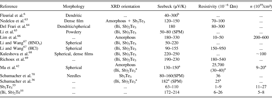
However, Sb2Te3 and the ternary compound Bi0.5Sb1.5Te3 as p-type semiconductors can potentially be used in electroplated TE devices. This section will cover both material classes, as the conditions for the deposition are quite similar, and several publications cover them simultaneously. Electrochemically, the deposition of the binary compound is simpler, as only the ratio between two elements needs to be controlled, similar to Bi2Te3. However, many researchers and publications are focused directly on the deposition of the ternary material, even though the composition in a three component system is obviously more difficult to control. This is likely due to the fact that Sb2Te3 shows inferior TE properties when compared to the ternary compound, especially a significantly lower Seebeck coefficient. The individual properties are covered in detail in the CRC Handbook of TEs,Reference Scherrer and Scherrer21 and a short summary of the properties is presented in Table II.
Overview of the achieved morphology, XRD orientation, and TE properties for various publications on (Bi, Sb)2Te3 film electrodeposition, comparison with the TE properties of (Bi, Sb)2Te3 fabricated by the traveling heater method. Apart from some exceptions, all the measurements were performed parallel to the surface (in plane) and then perpendicular to the film growth direction.
a Indicates values obtained for annealed material.
b Measured across the sample thickness.
SPM, done by Seebeck Probe Microsope
Finally, this section contains most of the same subsections as the previous section on Bi2Te3; however, the sections about the choice of seed layer and characterization methods are omitted, as they would contain essentially the same information and are, therefore, redundant.
A. Electrolyte
The reaction for the electrodeposition of Sb2Te3 was described by Leimkuhler et al.Reference Leimkuhler, Kerkamm and Reineke-Koch71 as,
 $$2{\rm{Sb}}{{\rm{O}}^ + } + 3{\rm{HTeO}}_2^ + + 13{{\rm{H}}^ + } + 18{{\rm{e}}^ - } \to {\rm{S}}{{\rm{b}}_{\rm{2}}}{\rm{T}}{{\rm{e}}_{\rm{3}}} + 8{{\rm{H}}_{\rm{2}}}{\rm{O}}\quad .$$
For the fabrication of ternary compounds, the overall deposition reaction for any desired composition, Bi2−xSbxTe3, can be described as,Reference Li, Soliman, Zhou, Toprak, Muhammed, Platzek, Ziolkowski and Muller65,Reference Qiu, Zhou, Cheng and Ahuja72
 $$(2 - x){\rm{B}}{{\rm{i}}^{3 + }} + x{\rm{Sb}}{{\rm{O}}^ + } + 3{\rm{HTeO}}_{\rm{2}}^{\rm{ + }} + (9 + 2x){{\rm{H}}^ + } + 18{{\rm{e}}^ - } \to {\rm{B}}{{\rm{i}}_{2 - x}}{\rm{S}}{{\rm{b}}_x}{\rm{T}}{{\rm{e}}_3} + (6 + x){{\rm{H}}_{\rm{2}}}{\rm{O}}\quad {\rm{.}}$$
The first mention of the electrodeposition of Bi0.5Sb1.5Te3 is by Fleurial et al. in 1999.Reference Fleurial, Borshchevsky, Ryan, Phillips, Snyder, Caillat, Kolawa, Herman, Mueller and Nicolet6 Their electrolyte was based on 1 M HNO3 and an unspecified complexing agent used to increase the solubility of Sb in the solution. The electrolyte was very similar to the one used for the deposition of Bi2Te3 and lead to stoichiometric ternary materials with moderate to high positive Seebeck coefficients. The earliest work on the electroplating of Sb2Te3 was conducted by Leimkuhler et al. in 2002,Reference Leimkuhler, Kerkamm and Reineke-Koch71 originally intended for use as a contact material for CdTe solar cells. Their work was based on a KCl-based electrolyte, and the deposition was conducted near the boiling temperature of the plating bath. The mentioned low solubility of Sb+III is a general problem for the fabrication of reasonably high concentrated electrolyte solutions and is nearly universally solved by the addition of a complexing agent. This complexing agent is typically either tartaric acid or citric acid, with concentrations between 0.1 and 0.84 M. The resulting complex in the case of tartaric acid can be written as [Sb2(C4H4O6)2]2+.Reference Ma, Ahlberg, Sun, Iversen and Palmqvist42 A notable exception is the use of chloride-based electrolytes (HClReference Nedelcu, Sima, Manea, Lazarescu, Ghita, Craciunoiu and Visan63 or KClReference Leimkuhler, Kerkamm and Reineke-Koch71), where chloride ions are considered as chelating reagents of the cation species. Typical Sb ion concentrations for most publications are in the range of ∼5–20 mM, in conjunction with Te ion contents usually around values of 10 mM. For the ternary compounds, the Bi ion content is typically chosen between 1 and 2 mM. For similar deposition conditions, a higher content of Bi or Sb ions in the electrolyte will lead to a higher concentration of the respective element in the deposited film (see e.g., Refs. Reference Del Frari, Diliberto, Stein, Boulanger and Lecuire64 and Reference Del Frari, Diliberto, Stein, Boulanger and Lecuire73). Schoenleber et al. have studied the influence of the presence of tartaric acid on the diffusion of bismuth, tellurite, and antimony cations.Reference Schoenleber, Stein and Boulanger33 It appears that the relationship between the compounds Sb2Te3 and Bi0.5Sb1.5Te3 and their synthesis bath, based on diffusion considerations, does not match with the used electrolytes in the literature data. They underline that the electrodeposition of compounds with antimony is not obvious; the difficulty should come not only from the limited diffusion of the cation SbIII but also to the coreduction of additional phases.
The electrolyte basis is less standardized than for the case of Bi2Te3, and while several publications are based on similar 1 M HNO3 solutions, both hydrochloric and perchloric acid are also frequently used as the supporting electrolyte. The most typical acid concentration is 1 M, with higher concentrations occasionally applied to achieve higher ion content.Reference Lim, Kim and Oh66 No significant influence was observed between the used acids on the morphology and the properties of the deposits. Films with good properties have been electroplated in HCl,Reference Li and Wang67 or HNO3 and HClO4-based solutions (e.g., Refs. Reference Richoux, Diliberto and Boulanger69 and Reference Schumacher, Reinsberg, Akinsinde, Zastrow, Heiderich, Toellner, Rampelberg, Detavernier, Broekaert, Nielsch and Bachmann70).
An organic electrolyte, based on dimethyl sulfoxide (DMSO) and KNO3, has been investigated by Li et al.Reference Li and Wang74,Reference Li, Wang, Gong and Li75 and can also be used for the deposition of smooth (Bi, Sb)2Te3 films with the targeted stoichiometry. However, as DMSO is a potent solvent for most photoresists, this electrolyte is not necessarily well suited for microfabrication processes. Tittes and PliethReference Tittes and Plieth76 demonstrated the possible use of an alkaline electrolyte, based on potassium diphosphate, with good results. Similar to organic electrolytes, though, the stability of photoresists in the alkaline solutions might be problematic. More recently, the electrodeposition of binary SbxTey films in molten acetamide mixtures was demonstrated with positive Seebeck coefficients of +80 µV/K.Reference Nguyen, Peng, Murugan, Vullers, Vereecken and Fransaer77
1. Additives
Since the as-deposited films are rough or dendritic in some cases, several publications are focused on the effect of additives, and primarily surfactants intended to improve the morphology of the deposited films, i.e., to make them more homogeneous. Examples are given in the work of Lim et al.,Reference Lim, Kim and Oh66 who used ethylenediaminetetraacetic acid, Kuleshova et al.,Reference Kuleshova, Koukharenko, Li, Frety, Nandhakumar, Tudor, Beeby and White68 who used sodium ligninsulfonate, and Yoo et al.,Reference Yoo, Song, Lim, Myung, Lee, Oh, Lee, Kim, Kim, Choa, Lee, Lee and Lim78 who investigated the effect of cetyltrimethylammonium bromide. For all cases, the addition of the surfactant led to a significantly improved morphology of the deposited films.
B. Deposition
The deposition of Sb2Te3 and Bi0.5Sb1.5Te3 compounds has been successfully conducted under both potentiostatic as well as galvanostatic conditions, as well as potential and current-controlled pulsed methods. However, due to the difficult control of the stoichiometry for these compounds, the majority of publications focus on potential-controlled methods, primarily potentiostatic deposition.
A thorough comparative study of the Bi2Te3, Sb2Te3, and (Bi, Sb)2Te3 deposition under potentiostatic conditions was e.g., published by Del Frari et al.Reference Del Frari, Diliberto, Stein, Boulanger and Lecuire73 Another interesting example is the work of Jung and Myung,Reference Jung and Myung79 who systematically investigated the electroplating of Sb2Te3 using electrochemical quartz microbalance and rotating disc electrode techniques. One main conclusion of their work was the importance of electrolyte agitation for the deposition of crystalline materials.
The main challenge for current-controlled deposition is the significant difference in reduction potential between Sb and Te, as discussed e.g., by Li et al.,Reference Li, Soliman, Zhou, Toprak, Muhammed, Platzek, Ziolkowski and Muller65 Lim et al.,Reference Lim, Kim and Oh66 or Li and WangReference Li and Wang67 This effect leads to very pronounced changes in the composition even for small changes in the deposition current. Nonetheless, the galvanostatic deposition of Sb2Te3 with the desired composition was reported by Huang et al.,Reference Huang, Kellock and Raoux80 and ternary compounds were reported by Lim et al.Reference Lim, Kim and Oh66
The validity of pulsed, current-controlled deposition was thoroughly investigated by Del Frari et al.Reference Del Frari, Diliberto, Stein, Boulanger and Lecuire64 and in a later, related publication by Richoux et al.Reference Richoux, Diliberto and Boulanger69 The first work investigated the effect of pulsed plating with comparatively long pulse durations between 0.5 and 10 s, and the best results were achieved with on and off times of 5 s each. The work by Richoux et al. explored a larger range of pulse durations, ranging from 20 ms to 5 s, and the effects of the various pulse parameters on the stoichiometry and morphology of the deposited material were identified. It was concluded that pulsed deposition can be used to improve the TE properties, as well as the morphology of the materials.
The pulsed, potential-controlled deposition has been investigated by Schumacher et al.Reference Schumacher, Reinsberg, Akinsinde, Zastrow, Heiderich, Toellner, Rampelberg, Detavernier, Broekaert, Nielsch and Bachmann70 and led to improved crystallinity and morphology in the deposited films. The optimal pulse length was given as 10 ms, with a corresponding relaxation time of 50 ms, and a slow (1 Hz), controlled stirring rate of the electrolyte.
Ma et al.Reference Ma, Ahlberg, Sun, Iversen and Palmqvist42 applied a mixed pulsed method, with a potential-controlled deposition pulse and a current-controlled resting pulse. The pulse duration was 1 s, with a relaxation time of 10 s; however, only films with a thickness of less than 1 µm were achieved.
C. Deposited material
As will be discussed in detail within this section, the deposition of Sb2Te3 and (Bi, Sb)2Te3 compounds is unfortunately rather difficult, particularly with respect to the morphology and the crystallinity.
1. Composition
The composition of the binary compound can essentially be controlled by adjusting the ratio of ions in the electrolyte (see e.g., Ref. Reference Huang, Kellock and Raoux80) or by adjusting the deposition conditions, i.e., either the deposition potential or the applied current density. This work is analogous to the deposition of binary Bi2Te3 and is mostly unproblematic.Reference Del Frari, Diliberto, Stein, Boulanger and Lecuire73 One challenge is the strong dependence of the composition on the applied potential or current, which is more pronounced than for the deposition of Bi2Te3. This can possibly be attributed to the significantly lower binding energy of Sb2Te3, as described by Schumacher et al.Reference Schumacher, Reinsberg, Akinsinde, Zastrow, Heiderich, Toellner, Rampelberg, Detavernier, Broekaert, Nielsch and Bachmann70 The deposition of binary materials with the correct composition, while challenging, can be considered to be a state-of-the-art process. The deposition of ternary compound is significantly more difficult, as the correct balance between three individual components needs to be achieved. This typically requires the adjustment of the electrolyte composition in addition to finding the correct deposition conditions. One possible procedure to fully control the film composition is outlined in the work of Del Frari et al.Reference Del Frari, Diliberto, Stein, Boulanger and Lecuire73 and is based on adjusting the Sb to Bi ratio in the electrolyte. Unlike the deposition of the binary compounds, the full compositional control in the ternary compounds cannot be considered to be state-of-the-art and remains a challenge.
2. Morphology
Even if the film composition of the Sb2Te3 and (Bi, Sb)2Te3 compounds can be finely tuned, their morphology is one of the main challenges. While several different variations of the growth mechanism and resulting film morphology have been established in the literature (for examples see Refs. Reference Golgovici, Cojocaru, Anicai and Visan28, Reference Jung and Myung79, and Reference Park, Xiao, Yoo, Rheem and Myung81), they are nearly universally inadequate for practical applications, as they lead to discontinuous and extremely rough films.
Several different approaches to improve the morphology have been reported in the literature, with the three most prominent being the addition of surfactants (e.g., Refs. Reference Kuleshova, Koukharenko, Li, Frety, Nandhakumar, Tudor, Beeby and White68 and Reference Yoo, Song, Lim, Myung, Lee, Oh, Lee, Kim, Kim, Choa, Lee, Lee and Lim78), the application of suitable pulsed electroplating protocols (e.g., Refs. Reference Del Frari, Diliberto, Stein, Boulanger and Lecuire64 and Reference Richoux, Diliberto and Boulanger69) and finally, the application of controlled stirring conditions (e.g., Refs. Reference Schumacher, Reinsberg, Akinsinde, Zastrow, Heiderich, Toellner, Rampelberg, Detavernier, Broekaert, Nielsch and Bachmann70 and Reference Jung and Myung79). All of these approaches have led to significant improvements in the deposited films; however, there is no obvious agreement in the literature about the best method. The identification of a simple, reliable, and repeatable approach for improving the morphology of the deposited materials is, therefore, a challenge that does not seem to be fully solved yet.
3. Thickness
The typical reported deposition thickness for the Sb2Te3 and (Bi, Sb)2Te3 materials is around a few micrometers and, therefore, significantly lower than for Bi2Te3 compounds. These low thickness values are related to bad morphology, as thin layers are typically still interconnected and can, therefore, be characterized.Reference Li, Soliman, Zhou, Toprak, Muhammed, Platzek, Ziolkowski and Muller65 The highest thickness values of 20 µm were reported by Del Frari et al.,Reference Del Frari, Diliberto, Stein, Boulanger and Lecuire64 however, with a very large associated roughness of ∼12 µm. Structured Sb2Te3 thermolegs with a thickness of 20 µm and good morphology were reported by Snyder et al.Reference Snyder, Lim, Huang and Fleurial82 and Kim and Oh.Reference Kim and Oh83
4. Crystallinity
The crystallinity of the deposited materials is analyzed in the majority of the available publications, with varying and not consistent results. Most publications report the existence of a crystalline phase of the deposited material, usually with a random orientation. This is in strong contrast to the results obtained for the deposition of Bi2Te3, which typically shows a strong preferred (110) orientation. Several reports indicate partly or even fully amorphous materials (e.g., Refs. Reference Ma, Ahlberg, Sun, Iversen and Palmqvist42 and Reference Lim, Kim and Oh66). The crystallinity can be significantly improved by applying a pulsed deposition protocol, as described by Schumacher et al.Reference Schumacher, Reinsberg, Akinsinde, Zastrow, Heiderich, Toellner, Rampelberg, Detavernier, Broekaert, Nielsch and Bachmann70 These results indicate that the growth mechanism and the applied deposition conditions have a strong influence on the crystallinity of the material.
It seems likely that the crystallinity and morphology of the deposited materials are to a certain extent interrelated and also need to be optimized in conjunction. However, no ideal recipe is readily available in the literature, and the growth mechanisms do not seem to be fully understood yet.
D. TE properties
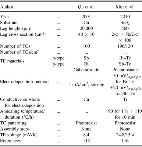
Table II gives an overview of the measured TE properties of electroplated Sb2Te3 and (Bi, Sb)2Te3 films found in the literature. The lack of an interconnected layer with a defined thickness complicates the electrical characterization of the deposited films, with the exception of the Seebeck coefficient, for which the morphology is less important. This is also a likely reason for the small amount of available electrical measurement results (including Hall measurements) on these films.
1. Seebeck coefficient
Regardless of the exact composition, all reported Seebeck values for both the binary Sb2Te3 and the ternary (Bi, Sb)2Te3 compounds are positive, indicating the expected p-type conductivity for these materials. The range of reported values for the Seebeck coefficient is, however, very large with values between 40 and 330 µV/K. This large spread is probably related to the different crystallinities of the deposited materials, as discussed in the previous section. For fully amorphous films, or films with a higher content of amorphous material, the Seebeck coefficient would be expected to be higher, while fully crystallized materials should typically exhibit lower values (e.g., Refs. Reference Lim, Kim and Oh66 and Reference Yoo, Song, Lim, Myung, Lee, Oh, Lee, Kim, Kim, Choa, Lee, Lee and Lim78). Other effects, like the precise composition, the deposition conditions and the different morphologies will, however, also influence the measured values, and therefore, general trends are difficult to identify (e.g., Refs. Reference Li and Wang67 and Reference Schumacher, Reinsberg, Akinsinde, Zastrow, Heiderich, Toellner, Rampelberg, Detavernier, Broekaert, Nielsch and Bachmann70).
2. Carrier concentration
The determination of the carrier concentration, as well as the electrical resistivity, is complicated by the common lack of a homogeneous, interconnected layer. The few available articles, which report on the carrier concentration for the p-type materials, consistently place the values in the range of 1021 to 1022/cm³ (e.g., Refs. Reference Lim, Kim and Oh66 and Reference Kuleshova, Koukharenko, Li, Frety, Nandhakumar, Tudor, Beeby and White68). These values are consistent with the theoretical expectations for highly disordered and partly amorphous materials. Similar to the Bi2Te3 films discussed previously, the high-carrier concentration in Sb2Te3 and Bi0.5Sb1.5Te3 films is frequently coupled with low carrier mobility, indicated by the high values for the electrical resistivity.
3. Electrical resistivity
The values reported for the electrical resistivity range from 10 to 1000 µΩm, with one extreme value of 25,700 µΩm.Reference Ma, Ahlberg, Sun, Iversen and Palmqvist42 The most commonly encountered range of values lies between ∼50 to 250 µΩm. This large spread is consistent with the high variance of the other electrical properties and is again probably related to the difference in crystallinity and the different morphologies resulting from the various fabrication conditions. The carrier mobility is correspondingly low, with reported values on the order of 10–50 cm²/Vs for both Sb2Te3 and Bi0.5Sb1.5Te3 films.Reference Kuleshova, Koukharenko, Li, Frety, Nandhakumar, Tudor, Beeby and White68,Reference Lim, Park, Lim, Yoo, Lee, Myung and Lee84 For many materials with high resistivity values, it can be expected that the mobility is even significantly lower. This low mobility and the correspondingly high electrical resistivity in these compounds is, in addition to the morphology, the second main challenge for their application in TE applications.
4. Annealing
Annealing of the deposited materials offers a possible solution for the low mobility of the materials, as it would be expected to increase the crystallinity and, therefore, the carrier mobility. As a consequence, the electrical resistivity should also improve, even though this could potentially be partly countered by a corresponding decrease in carrier concentration through the decreased defect density.
The effect of an annealing treatment on the crystallinity of Sb2Te3 was investigated by Huang et al.,Reference Huang, Kellock and Raoux80 and it was found that an annealing temperature of 120 °C is already sufficient for the crystallization of amorphous starting material. Park et al.Reference Park, Xiao, Yoo, Rheem and Myung81 also observed a transition from amorphous to crystalline material for (Bi, Sb)2Te3 films, although they used an annealing temperature of 250 °C. They additionally reported a corresponding increase in the mobility of their films. Li and WangReference Li and Wang74 observed an improvement in both the Seebeck coefficient as well as the electrical resistivity after a temperature treatment at 250 °C for 4 h in inert N2 atmosphere.
An increase in the average grain size, identified by XRD measurements, and an improvement in the electrical resistivity were reported by Lim et al.,Reference Lim, Park, Lim, Myung, Lee, Jeong, Yoo and Lee85 and similar results were also reported by Ma et al.Reference Ma, Ahlberg, Sun, Iversen and Palmqvist42 and Schumacher et al.Reference Schumacher, Reinsberg, Akinsinde, Zastrow, Heiderich, Toellner, Rampelberg, Detavernier, Broekaert, Nielsch and Bachmann70
An annealing treatment is, therefore, beneficent for the electrical properties of the electroplated Sb2Te3 and (Bi, Sb)2Te3 materials. Overall, the improvements seem most pronounced in the electrical resistivity and carrier mobility, while the change in the Seebeck coefficient of the materials is less distinct. However, similar to Bi2Te3, the evaporation of tellurium from the compound was reported to slightly change the composition of the compound,Reference Ma, Ahlberg, Sun, Iversen and Palmqvist42 indicating that a controlled annealing might be required.
This approach was experimentally investigated by Schumacher et al.Reference Schumacher, Reinsberg, Rostek, Akinsinde, Baessler, Zastrow, Rampelberg, Woias, Detavernier, Broekaert, Bachmann and Nielsch36 by annealing (BixSb1−x)2Te3 films in a saturated Tellurium atmosphere. The results demonstrated that this equilibrium annealing not only prevents the evaporation of Te but can also be used to control the composition of the material. The TE properties of the materials were significantly improved with final Seebeck coefficients on the order of ∼180 µV/K carrier concentrations around 8∣1019/cm³ and carrier mobility of ∼30 cm²/Vs.
IV. DEVICE FABRICATION FOR ELECTROPLATED MICROSCALE TE GENERATORS
Over the past decade, driven by the requirements of power generation and cooling in microelectronic devices, recent works have been conducted to promote the development of microscale TE device based on thin films. Microscale TE devices have numerous advantages when compared to standard macroscopic devices. Most obvious among these is the smaller size, which allows the integration into smaller systems. Due to the smaller structure size, which is accessible through microfabrication techniques, the integration density in these devices can be significantly higher, i.e., a significantly larger number of TE couples can be implemented. This leads to higher output voltages, especially for small temperature differences, and simplifies the electrical interface. Finally, microscale devices exhibit higher power densities, caused by the thinner thermocouples and correspondingly higher possible heat flux.Reference Fleurial, Borshchevsky, Ryan, Phillips, Snyder, Caillat, Kolawa, Herman, Mueller and Nicolet6 One of the main disadvantages of these devices is the complex and expensive fabrication method. Additionally, the limited height of the TE materials requires a highly conductive substrate material and excellent thermal contacts to minimize performance and heat losses.
TE generators have been manufactured by various microfabrication methods with V2VI3 compounds obtained by hot pressing,Reference Kishi, Yoshida, Okano, Nemoto, Funanami, Yamamoto and Kanazawa86,Reference Kishi, Nemoto, Hamao, Yamamoto, Sudou, Mandai and Yamamoto87 by sputtering,Reference Stordeur and Stark88–Reference Bottner92 by MOCVD,Reference Venkatasubramanian, Siivola, Colpitts and O'Quinn93,Reference Chowdhury, Prasher, Lofgreen, Chrysler, Narasimhan, Mahajan, Koester, Alley and Venkatasubramanian94 with poly-Si and poly-SiGe thermolegs by a CMOS compatible fabrication process,Reference Strasser, Aigner, Franosch and Wachutka95,Reference Strasser, Aigner, Lauterbach, Sturm, Franosch and Wachutka96 and with poly-Si and Al thermocouples by CVD and microelectromechanical systems (MEMS) fabrication process.Reference Huesgen, Woias and Kockmann97 However, in the context of this review, we focus the presentation on the reported fabrication methods for TE generators using electroplating as a deposition method.
Compared to conventional microfabrication methods, like sputtering, evaporation, or epitaxial growth, the electroplating of the TE materials offers several advantages. One of them is the cost efficiency of the process and the necessary equipment. As electroplating is primarily used to grow the desired structures into a photoresist template, there is practically no waste of material, since the deposition only takes place in the desired areas. Conventional methods, on the other hand, typically deposit material on the whole substrate and parts of the equipment, which creates a significant amount of wasted material. This is particularly undesirable in the case of expensive or toxic materials, like gold, platinum, or tellurium. The necessary equipment is also usually easier to implement, as the deposition basically only requires an electrolyte bath, a sample holder, and a potentiostat, as well as some basic accessories (e.g., cleaning and rinsing, stirring, reference electrode, etc.). Due to these advantages and high-growth rates (a few µm/h for V2VI3), electroplating allows the deposition of significantly higher material thicknesses than conventional methods, up to layers which are several hundred micrometers thick. This is especially advantageous for the case of microfabricated TE generators, where a certain material thickness is required to achieve a reasonable thermal device resistance.
There are, however, several challenges, which need to be addressed to use electroplating as a fabrication method for microscale devices. To take advantage of the selective deposition process, an electrically conductive seed layer, as well as a suitable template for the growth, is needed. Particularly for high-material thickness or large aspect ratios, the fabrication of a suitable template can be difficult.
The necessity of a seed layer is especially challenging for the fabrication of TE devices, as the electrical connection required for the seed layer is different from the one required in the final device. This is due to the fact that an electrical connection is needed between the two different materials in the device, while the electrodeposition of two different materials would ideally be conducted onto two electrically separate seed layers.
Rapidly, after the first investigations on electroplated Bi2Te3,Reference Takahashi, Oda, Ogino and Furuta1,Reference Magri, Boulanger and Lecuire4 the interest of electrochemistry was detected in view of microproducts as well as microfabrication methods.
A. Feasibility experiments
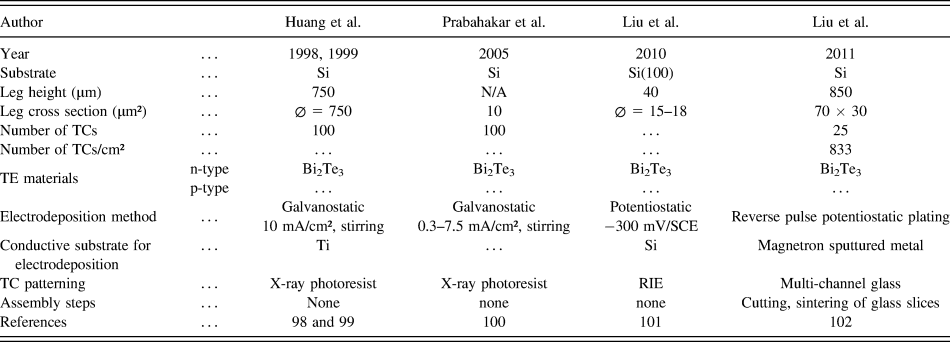
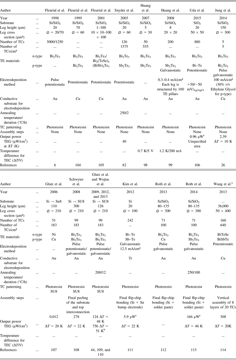
Structuring of the deposited material is an essential prerequisite for the fabrication of TE devices. Before describing the different approaches for the fabrication of TE devices, we will first start with a brief overview (Table III) of some preliminary experiments, which did not lead to a complete device but verified some general principles of patterning technology either in organic photoresist or silicon templates and demonstrated the feasibility of depositing the materials into microstructured templates.
Feasibility studies of electroplated TE material microstructured templates.
The photoresist option was taken, starting in 1999, by the group of Murphy,Reference Huang, Wang and Murphy5 who fabricated leg elements via multistep LIGA technique for a thermoelectric cooler (TEC) for a biological use (neural probes). Smooth microposts of bismuth telluride alloy were obtained. The electroplating was performed through a patterned polymethylmethacrylate (PMMA) x-ray resist. The key points of this preliminary work concern the dimensions of the posts with an impressive height of 750 µm and a diameter of 150 µm, and especially their free standing after the removing of the remaining PMMA on the Titanium substrate. In 2005, a design of a prototype device consisting of an array of 100 TECs (10 µm width) was announced by this group for a use of cryosurgical or cryopreservation of cells without the finalization of the device being reached.Reference Prabhakar, Podlaha-Murphy, Murphy, Devireddy, Laurencin and Botchwey100
Another way for structuring TE legs was chosen by Liu et al.Reference Liu, Xu and Li101 Some microtemplates with vertical hole arrays (15–18 µm in diameter and 40 µm in depth) were fabricated on p-Si(100) with photolithograph and reactive ion etching with the goal of achieving a surface-perpendicular thermopile. Afterward, a potentiostatic deposition is conducted at –300 mV/SCE in a solution containing 0.01 M Bi3+ and 0.01 M HTeO2+. However, the thermal conductivity of silicon is so high that it can be a drawback to a good energy conversion. For the final use, a template removing process with RIE etching is required after the electroplating, and the pillars can stand free. In 2011, the same authors proposed another concept with a multichannel glass template (Fig. 3).Reference Liu and Li102 The main advantage of the glass template lies in its low-thermal conductivity and its electrical insulator character, allowing to keep it even after TE compound filling. The principle is based on a molding method by combining mechanical cutting [Fig. 3 (a)], sintering with press of glass slices [Figs. 3 (b-d)], and a reverse-pulse electrochemical filling of the microscale array [Fig. 3 (e-i)]. The schematic overview is fully described but only n-type arrays were prepared. The pillars (850 × 70 × 30 µm) have a resistance of 4.05 Ω comparable to bismuth telluride bulk material.
Fabrication process flow schematic for the generator fabrication process applied by Liu and Li. make flutes on glass slices by cutting (a), pile up and sinter the glass slices with press from top and bottom (b), cut the as-sintered glass template into required length (c, d), magnetron sputter the deposition electrodes on a silicon wafer (e), bond the template with the wafer (f), electrodeposit N-type thermoelectric array with one half of the interdigital electrodes connected to the cathode (g), electrodeposit P-type thermoelectric array with the other half of the interdigital electrodes connected to the cathode (h), remove the substrate wafer and make the connection electrodes for the thermoelectric device on both top and bottom side of the template (i) (Figure taken from Ref. Reference Liu and Li102 reproduced by permission of Springer).
All these works are based on a one-substrate concept with successive deposition of p- and n-type compounds after patterning. A different approach to designing TE microgenerators is a process developed by MicroPelt.Reference Bottner90–Reference Bottner92 It is based on a two-wafer concept, and involves the deposition, structuring and annealing of the n- and p-type materials onto separate substrates, which are then flip chip bonded during the final assembly step. The key advantage of this method is that both materials can be optimized completely independent of each other, specifically with respect to any high-temperature processing steps, like e.g., the annealing. The main challenge is the bonding step, which requires a precisely controlled thickness of the TE materials and a suitable solder or bonding material. While the process in its final version does not actually involve any electrodeposition steps, electroplating of the TE materials was considered and tested as a fabrication route, as discussed in a publication by Diliberto et al.Reference Diliberto, Michel, Boulanger, Lecuire, Jagle, Drost and Bottner103 The possibility of a full wafer deposition of Bi2Te3-based materials, as well as wet chemical and reactive ion etching for the structuring of the films, was successfully demonstrated.
B. Processes of complete device fabrication
Several different approaches for the fabrication of TE devices (coolers or generators), which exploit the advantages of the electroplating process and simultaneously solve the associated challenges, have been demonstrated in the literature and will be discussed in the following sections. A double classification of a micro-TE generator can be established from its design setup, in particular, the heat flow direction through the device (in-plane or cross-plane configuration) and the layout of thermocouples (TCs) (laterally or vertically fabricated TCs). A schematic diagram (Fig. 4) taken from the paper of Glatz et al.Reference Glatz, Schwyter, Durrer and Hierold44 explains the different types: type A-lateral/lateral, type B vertical/lateral, and type C vertical/vertical. In planar devices, heat flows along the surface, laterally through the TE materials, which is beneficial to get higher output voltage and output power. If the planar configuration has the advantage of an easier formation of thin film legs and offers a very convenient way of fabricating electrical interconnects between the thin films legs, the substrate will act as a thermal short that reduces performances. The vertically integrated refers to a design eliminating the large heat losses observed in planar thin film TE devices, where legs are deposited onto a supporting substrate. In a vertical design, a temperature difference between the top and bottom surfaces generates the TE response. But the drawback is the small temperature difference depending on the thickness of the legs, so a low voltage is generally generated along the cross plane direction. Thicker legs give a higher voltage. The vertical heat flow is driven by the improved thermal contact proportional to the contact surface area to heat source and sink. Moreover, by going to a lateral to a vertical design, higher packing densities of the thermocouple pairs can be achieved resulting in higher responses per unit area. In conclusion, the cross-plane type has the advantages of low-electrical resistance, no parasitic heat flow through a substrate and an improvement of thermal contact to heat source and sink, the possibility of higher integration densities and output power.
Design approaches for µ TEG (a) lateral/lateral-type; (b) vertical/lateral -type; (c) vertical/vertical type (figure taken from Ref. Reference Glatz, Schwyter, Durrer and Hierold44 reproduced by permission of IEEE).
The state-of-the-art evidences a majority of type-C design, which allows for a denser packaging of thermocouples. The review will start with them, we will refer to one example of type-B, and finally, we will end with some examples of type-A. A summary of the characteristics (materials, design, and performances) of the electroplated microscale TE generators is given in Tables IV and V. The most thoroughly studied material is bismuth telluride for n-type. One of the main challenges in the fabrication of p-type is the dendritic growth mode (discussed e.g., by Lim et al.Reference Lim, Snyder, Huang, Hennan, Ryan and Fleurial43), which is presumably the reason for a distribution between the binary compounds Bi2Te3, Sb2Te3, and the ternary compound (BiSb)2Te3.
Electroplated cross-plane TE devices with vertical heat flow direction and vertical layout of TE material (except for Wang et al.)
a Vertical heat flux and lateral layout of TE material.
b Annealed material.
c Output power with unspecified area.
Electroplated in-plane TE device with lateral heat flow direction and lateral layout of TE material.
1. Type C: Cross-plane devices (vertical/vertical)
In the category of vertical/vertical devices, several different fabrication processes for the fabrication of micro-TE generators, with different fundamental principles, have been established in the literature. There are three basic different approaches for creating the necessary structures.
One is the use of a single substrate and a positive type photoresist, which can be structured several times and can finally be removed. This allows for the successive deposition of the materials and an eventual restructuring of the lower contact structure. The second approach is the use of a permanent photoresist, which doubles as a substrate, and allows the device to be accessed and structured from both sides. This allows for a selective deposition by using structured seed layers, and a full restructuring of this seed layer into the lower contact structures. The third one is the inclusion of a flip-chip bonding step, which allows for a separate structuring of the n- and p-type materials and contact structures.
Each of these approaches has its advantages and disadvantages, and can potentially be used for different applications. Key differences can be found in the choice of substrate materials, process complexity, choice of applicable photoresists, and number of lithography steps. None of the demonstrated published processes offers the “ideal” combination of high-thickness thermocouples, simple fabrication, and a fully removable photoresist template.
The first study carried out to confirm the potential of TE compound electroplating for the entire fabrication of microcoolers was presented in 1998.Reference Fleurial, Borshchevsky, Ryan, Phillips, Snyder, Caillat, Kolawa, Herman, Mueller and Nicolet6 The process developed at the Jet Propulsion Laboratory (JPL) at the California Institute of Technology is based on the successive deposition of the n- and p-type materials into the same photoresist template on a single wafer.Reference Lim, Snyder, Huang, Hennan, Ryan and Fleurial43,Reference Snyder, Lim, Huang and Fleurial82,Reference Fleurial, Snyder, Herman, Smart, ShakkottaI, Giauque and Nicolet104,Reference Borshchevsky, Caillat, Fleurial, Kolawa, Olson, Philips and Ryan105 The fundamental concept is based on the use of a positive type photoresist, which allows for multiple consecutive structurization steps, as long as all processing is conducted under yellow light conditions. The process was intentionally developed with the goal of electrochemical deposition for the TE and contact materials, and therefore, takes full advantage of the possibility of template-based growth.
The schematic process flow, as published by Snyder et al.,Reference Snyder, Lim, Huang and Fleurial82 is shown in Fig. 5. First, the lower contact material, a 3-µm thick gold layer, is electroplated into a conventional photoresist template, using a thin chrome layer as the seed layer [Fig. 5(a)]. A thick positive type photoresist, with a thickness of up to 40 µm, is then spin-coated on the substrate, and the template for the deposition of the first set of TE legs is lithographically opened [Fig. 5(b)]. The first TE material is then deposited into the template [Fig. 5(c)]. Next, a thin layer of photoresist is used to cover the already deposited material, and then the holes for the second TE material are opened. The second set of thermolegs can then be deposited into the template, while the first set of legs is protected from the electrolyte by the thin second photoresist [Fig. 5(d)]. The second thin photoresist layer is then removed by a short flood exposure and development, and a thin layer of gold is sputtered onto the structure to serve as seed layer for the upper contacts. A new layer of photoresist is then deposited and structured, and serves as the template for the deposition of the upper contact, which consists of 3 µm of low stress nickel [Fig. 5(e)]. The unnecessary layers (upper photoresist, thin-sputtered gold layer, thick photoresist, and chrome seed layer) are then removed by a suitable combination of solvents and etching steps, creating the final freestanding device [Fig. 5(f)].
Fabrication process flow schematic for the generator fabrication process applied by Snyder et al. (figure taken from Ref. Reference Snyder, Lim, Huang and Fleurial82 reproduced by permission of Nature Publishing Group).
This process offers several key advantages, e.g., that the fabrication is fully conducted on a single substrate, uses mainly conventional microfabrication techniques, and finally leads to a fully freestanding TE device without any thermal shunts. However, there are also some challenges, mainly the necessity of positive type photoresists, which offer only limited chemical resistance. Additionally, the overall process is fairly complex, as it involves several, sometimes unconventional, photolithography steps. The fabricated demonstration device contained 126 TE elements (n-Bi2Te3 and p-Sb2Te3, with a diameter of 60 µm and a height of 20 µm, and overall dimensions of ∼2 × 2 mm. The combined Seebeck coefficient of a thermocouple was ∼160 µV/K.
Huang et al.Reference Huang, Li, Chen, Zeng and She98 have followed a similar process integration by using electroplating and MEMS technology with four positive masks and photoresists. The column-type micro-TE cooler is constituted by 50 pairs of Bi2Te3 and Sb2Te3 pillars, with a diameter of 30 µm and a thickness of only 5 µm. The principal differences in comparison with the former JPL process relate to the rotation of the cathode during the electrodeposition and the galvanostatic process with an accurate current controller, both to enhance the density and the uniformity of TE deposits. The infrared thermal image measuring system showed an average cooling of about 0.7 K for the integrated µ-TEC under 5 volts driven. A variation of this process was proposed by the same group in 2008.Reference Huang, Lin, She, Li, Chen and Kuo99 A μ-TEC is fabricated with clustered multipillar structures (20 µm wide—8 µm high) in a 6 × 6 mm chip area. Each leg involves 100 parallel Bi2Te3 micropillars with 100 parallel Sb2Te3 micropillars [Figs. 6(a) and 6(b)]. A temperature difference of 1.2 K was measured, a higher value than the temperature difference of the µ-TEC with legs made of single pillars.
(a) Schematic design of the column-type Bi2Te3/Sb2Te3 µ-TEC with clustered multipillar structure and (b) fabrication process flow schematic for the generator fabrication process applied by Huang et al. (Figures taken from Ref. Reference Huang, Lin, She, Li, Chen and Kuo99 reproduced by permission of Elsevier).
A group in KoreaReference Jung and Ko26 fabricated a thermoelectric generator (TEG) based on n- and p-type bismuth telluride legs according the JPL process. The synthesis by pulse plating of n-type is performed in an aqueous medium while the p-type compound is obtained using a solution with 30% v/v Ethylene Glycol. TEGs made of 5 thermocouples (150 µm in height and 300 µm in diameter) were structured in a SU-8 photoresist on a silicon substrate (covered by SiO2 300 nm/Ti 10 nm/Au 300 nm). The thermocouple has a Seebeck voltage of 141 µV/K, and the generator produced an output power of 24.36 nW/TC at temperature difference of 10 °C. These moderate performances are caused by a high internal electrical resistance (20 Ω per thermocouple).
More recently, Uda et al.Reference Uda, Seki, Saito, Sonobe, Hsieh, Takahashi, Terasaki and Homma106 proposed the fabrication of a microdevice (8 arrays of 110 TCs, 20 µm in height, 50 × 50 µm²) through a patterning process, schematically described without any experimental details about the patterning. Both legs of the TCs are made of BiTe compounds. If the composition of the n-legs is Bi2Te3 type, the composition of p-legs is far from a V2VI3 compound (Bi 62.4 and Te 37.6 at.%). The work focuses on the size of the upper electrodes connecting the TE legs. The authors claimed that a benefit for enhancing the performances of the device is observed with an umbrella-type configuration, the term meaning that the upper electrode size is larger than the cross section of legs. The first result evidenced that the open circuit voltage is twice as large and the generated power (0.96 µW) 4.5 times larger than that of the device with a smaller electrode. Nevertheless, the performance remains weak, certainly due to the high resistance (total resistance of 79 Ω) and to an incorrect stoichiometry for TE compounds. This preliminary work needs to be confirmed with optimized electroplated compounds.
The fabrication process developed at the ETH Zürich, later greenTEG as a spin-off of the ETH Zürich,Reference Glatz, Schwyter, Durrer and Hierold44,Reference Glatz, Muntwyler and Hierold107,Reference Schwyter, Glatz, Durrer, Hierold, Bright, Bourouina, Courtois, Desmulliez, Karam and Wang108 is based on utilizing a chemically very resistant and mechanically stable photoresist, SU-8, as both deposition template and “substrate” for the final device. This photoresist layer is processed on a handle wafer with a sacrificial adhesion layer but is removed from the wafer during the later processing steps. The final device is embedded in the SU-8 layer and even offers a certain degree of mechanical flexibility.
The process flow is schematically depicted in Fig. 7 and was initially validated by electrochemical deposition of Cu and Ni.Reference Glatz, Muntwyler and Hierold107 First, the plating electrodes are deposited and structured on top of the sacrificial layer [Fig. 7(a)]. These electrodes basically serve as the seed layer but are structured in a way, which allows the selective deposition of the n- and p-type TE materials. The next step is the application and structuring of the 190 µm thick SU-8 mold, which contains the holes for both types of TE legs [Fig. 7(b)]. The p- and n-type TE materials are then successively deposited into the respective cavities, and any overgrowth is removed by a polishing step [Figs. 7(c) and 7(d)]. The 20-µm thick electrical copper contacts between the thermolegs are then electroplated and structured via chemical etching [Fig. 7(e)]. To access the plating electrodes on the other side of the device, the sacrificial layer is then dissolved to release the SU-8 layer [Fig. 7(f)]. As the plating electrodes are not in the desired configuration, they are removed and the electrical interconnects necessary for a device are plated and structured instead, creating the final device [Fig. 7(g)]. In the case of Bi2Te3-based devices, gold is used instead of copper as the interconnect material, due to its higher chemical resistance and lower contact resistances.Reference Glatz, Schwyter, Durrer and Hierold44 The demonstrated Bi2Te3-based devicesReference Glatz, Schwyter, Durrer and Hierold44 contained 99 thermocouples with leg diameters of 210 µm and a height of 140 µm. The overall dimensions of the generator were ∼10 × 10 mm. The reported combined Seebeck coefficient of one thermocouple was 91 µV/K.
Fabrication process flow schematic for the generator fabrication process applied by Glatz et al. (a) Patterning of seed layer electrodes; (b) structuring of SU-8 mold; (c) selective ECD of Cu-thermolegs; (d) ECD of Ni-thermolegs; (e) the bottom interconnects between the different thermolegs are etched into a 20-_m thick electroplated Cu-layer; (f) release of SU-8 layer by removing the sacrificial layer. Flipping the SU-8 disk gives access to the plating electrodes; (g) patterning of top interconnects and bond pads. (figure taken from Ref. Reference Glatz, Muntwyler and Hierold107 reproduced by permission of Elsevier).
The greenTEG process is unique in several ways and offers some advantages over other fabrication methods. Due to the possibility of accessing and especially restructuring the lower layers during the process, it is possible to use negative type photoresists and separately structured deposition electrodes for the two materials. This avoids several photolithographic steps when compared to the previously discussed JPL process. Due to the use of SU-8, very high structures are possible, and the final device retains a certain amount of flexibility. However, there are also some inherent disadvantages, with the main one being the unavoidable thermal shunt through the resist template. The absence of an electrically insulating and mechanically stable substrate might also be problematic in some applications, although the device can obviously be bonded onto a substrate if desired.
In 2012, ETH Zurich and greenTEG enhanced the electroplated microscale TE generators and proposed an optimization concerning the output power performanceReference Wojtas, Schwyter, Glatz, Kuhne, Escher and Hierold109 by integrating a microfluidic heat transfer system. This integration reduces the interfacial thermal losses. The heat transfer system consists of copper microchannels and a polymer PMMA manifold distribution layer. The heat transfer system assembled onto the TE generator evidenced an output power of 1.47 mW/cm² at an applied temperature difference of 50 K. This was confirmed in 2013Reference Wojtas, Ruthemann, Glatz and Hierold110 with a device exhibiting a net output power of 126.3 mW/cm² with a module ZT of 0.1 and an applied temperature difference of 95 K, with the thickness of TE legs being reduced to 60–90 µm.
The process developed by Kim and Oh. from Hongik University—KoreaReference Kim and Oh83,Reference Kim and Oh111 is mostly based on a similar concept to the one applied by JPL, however, the upper contact structure is fabricated on a separate substrate, and then flip-chip bonded to the rest of the device. The fabrication process is shown in Fig. 8. The n- and p-type materials are deposited into a positive type photoresist, onto a nonstructured seed layer, and with successively opened deposition cavities for the thermolegs [Figs. 8(a)–8(e)]. To achieve a precisely controlled height, the legs are then polished, and a nickel/tin capping layer is then deposited for the bonding process [Figs. 8(f)–8(h)]. The seed layer, which also serves as the lower contact material, is then etched to form the lower contact structure by a third patterning of the thick photoresist layer [Fig. 8(i)]. The photoresist is then dissolved, forming the bottom substrate device structure without the upper contact [Fig. 8(e)]. The upper contact on the top substrate is structured in a similar manner and then bonded to the bottom substrate by use of an anisotropic conductive adhesive, forming the final device [Figs. 8(k)–8(m)].
Fabrication process flow schematic for the generator fabrication process applied by Kim and Oh (a) sputtering of the Ti/Cu/Ti metallization, (b) photoresist (PR) patterning, (c) electrodeposition of the BiTe legs, (d) PR patterning, (e) electrodeposition of the SbTe legs, (f) planarization, (g) PR patterning, (h) electrodeposition of the Ni/Sn capping layer, (i) PR patterning, (j) bottom electrode patterning, (k) PR patterning and electrodeposition of Sn on a Top substrate, (l) top electrode patterning, (m) flip chip bonding (figure taken from Ref. Reference Kim and Oh111 reproduced by permission of the Japan Institute of Metals and Materials).
This process offers some advantages over the ones already described above. One is the direct implementation of an upper substrate, which is potentially advantageous for some application scenarios. The second is the use of a fully thickened lower contact layer as the seed layer, which possibly makes the deposition process more reliable as the electrical resistance is lowered. However, the process is fairly complex, as it involves numerous photolithography steps in addition to planarization and flip-chip bonding. The final device contained 242 thermocouples, with a leg diameter of 100 µm and a height of 20 µm. The overall dimensions were ∼5 × 5 mm². The Seebeck coefficient for a thermocouple was, based on the material properties, estimated to be ∼545 µV/K (−59 µV/K for n-Bi–Te and 485 µV/K for p-Sb–Te).
According to the same concept of a flip chip bonding, a µTEG was developed by Roth et al. in 2013.Reference Roth, Rostek, Lenk, Kratschmer, Cobry and Woias112 The generator is obtained from electroplated material (n-type Bi2Te3 and Cu) on a silicon substrate using a process based on two negative photoresists (SU-8 and Ordyl). The upper contacts of 71 TCs (300 µm wide and 135 µm high on a total area of 1 cm²) were formed by a flip-chip process of silicon chip with a solder paste Bi57Sn42Ag1. One year later, Copper is replaced in the generator by Sb2Te3.Reference Roth, Rostek, Cobry, Kohler, Groh and Woias113 In this work, a thickness of 300 µm for electroplated antimony telluride legs is reported, which is larger than the previous one in the range of several microns. This large thickness with a good morphology and density of antimony telluride deposits was obtained by pulse plating (on-pulse for 20 ms at −32.2 mA/cm² and an off-pulse for 175 ms at 0 mA/cm²) and with two stirring modes during the plating. A first period up to 5 µm legs was conducted without stirring to ensure a good growth on the starting layer. After 5 µm, electroplating is carried out with stirring the electrolyte but without changing the current densities and the pulse durations. After the evaporation of 100 nm Ti and 100 nm Au as barrier/bonding layer on TE legs, a thermal annealing was performed for 100 h at 250 °C in tellurium atmosphere to reduce the electrical resistance by inducing a phase change from amorphous to crystalline state. The measured power output was equal to 166 µW at a temperature difference of 46 K (i.e., 0.08 µW/K2), a value nevertheless inferior to a TEG made with annealed Bi2Te3 and Cu.
2. Type B cross-plane devices (vertical/lateral)
An alternative approach of a vertical assembly of planar-electroplated TC modules was investigated by Wang et al.Reference Wang, Ji, Xu, Li, Visan and Golgovici114 to increase the integration density of thermocouples in a given volume. In this configuration (Fig. 9), the thermal gradient is applied at the extremities of the films. This work can be anchored in the concepts of Stordeur and Stark.Reference Stordeur and Stark88,Reference Stordeur117 The first step is the electrodeposition of n-type BiTeSe and p-type BiTeSb strips (3.6 mm long × 0.4 mm wide × 50 µm thick) and copper (as connecting layer) on a metallic substrate structured by photolithography. After electrodeposition, the chains of thermocouples are peeled off from the seed layer and bonded together with epoxy resin. The next steps are the successive in-series connections of two adjacent foils (by electroless plating of copper) at the end of the connecting layers by silver wires. To create the final device, the stack is placed between two hard thermal plates, contacting to heat sink and source. The bonding of thermal plates is performed by thermal conductive layers (the lithography process, the nature of hard plates, and thermal conductive layers are unspecified). The proposed multilayer generator consists of a stack of 8 layers, each of them with a number of 20 p-types legs and 21 n-type legs on it. The final result is a small compact generator (4 mm high × 25 mm wide × 1 mm thick) with 160 thermocouples. The characteristics of the presented device are its internal resistance (1.1 kΩ), its open-circuit voltage (660 mV), maximum output power, and corresponding power density under the temperature difference 20 K (77 µW–770 µW/cm3) at 25 °C. The principle interest of the work lies in the synthesis of high-quality TE legs due to a gyration of thin strips after horizontal plating. Nevertheless, the peeling of TE elements, which induces high-internal resistance, is a certain disadvantage.
Schematic fabrication process applied by Wang et al. (a) Views of the film-like TE component; (b) schematic view of the TE aggregation; and (c) schematic view of the partly encapsulated TE aggregation (captions and figures taken from Ref. Reference Wang, Ji, Xu, Li, Visan and Golgovici114 reproduced by permission of Elsevier).
3. Type A cross-plane devices (lateral/lateral)
Very few examples of horizontal assembly of electroplated Peltier modules can be founded in the literature. The concept was tested in 2001 by Qu et al.Reference Qu, Plotner and Fischer115 for an in-plane Bi–Sb generator, and more recently, for an in-plane BiTe–SbTe thermopile sensor (Fig. 10) by Kim and Oh,Reference Kim and Oh116 the latest piece of work that we would like to present in this section. After a metallization (sputtered Ti) onto a glass substrate [Fig. 10 (a)], p-SbTe and n-BiTe strips (2 and 5 µm thick) were potentiostatically plated [Fig. 10(b) and 10(c)] and patterned with photolithography. The titanium seed layer was etched in hydrofluoric acidic medium [Fig. 10 (d)]. The strips were embedded in a cured photoresist as an insulation layer [Fig. 10 (e)], and the device was finalized by the insertion of a heater element composed of trilayers (Ti/Cu/Ti) connected to the strips at the center of the sensor [Fig. 10 (f)]. Two devices were designed with either 196 pairs of legs of 50 µm-width or 130 pairs of 100 µm-width. The first one showed a sensitivity of 24.8 mV/K, while the second one reached 15.4 mV/K, the decrease is linked to the smaller number of pairs on the same area. Thicker strips (5 µm) enhanced the sensitivity up to 36.5 mV/K.
Fabrication process flow schematic for the generator fabrication process applied by Kim and Oh (a) sputtering of the Ti seed layer, (b) electrodeposition and patterning of the p-type Sb-Te legs, (c) electrodeposition and patterning of the n-type Bi-Te legs, (d) removal of the Ti seed layer, (e) formation of a photoresist insulation layer after exposing the sensor electrode pads, and (f) formation of a Ti/Cu/Ti thin film heater. (figure taken from Ref. Reference Kim and Oh116 reproduced by permission of Japan Institute of Metals and Materials).
Although out of the scope of the review, some preliminary attempts of TE nanowire-based device fabrication processes have been done. The works are based on the successful fabrication of arrays of nanowires through the template synthesis approach. The reader can find related information in the review paper by Martín-González et al.Reference Martín-González, Caballero-Calero and Díaz-Chao118 As example, the synthesis feasibility of n-type and p-type arrays of NWs has been demonstrated in 2002Reference Sander, Gronsky, Sands and Stacy119 and 2003,Reference Martin-Gonzalez, Prieto, Gronsky, Sands and Stacy120 respectively. On opposite to the works related, the film based devices, less work, have been performed on the development of nanodevices. It can be mentioned, nevertheless a device made of electrodeposited n-type Bi2Te3 and p-type BiSbTe nanowires in alumina,Reference Lim, Whitacre, Fleurial, Huang, Ryan and Myung121 the design of nanomicrogenerator composed of n-type and p-type Bi2Te3 nanowire arrays in alumina,Reference Wang, Jia, Huang and Zhang122 a hybrid nanowire BiSb in porous alumina-bulk Bi0.4Sb1.6Te3 TE device,Reference Keyani, Stacy and Sharp123 a thermoelectrically cooled giant magnetoresistance sensor p-type BiSbTe or n-type BixTey nanowires grown in polycarbonate or alumina templates.Reference Davis, Bellamkonda and Mannam124
V. CONCLUSION
In this review, it has been shown that the electrochemical deposition of both n-type and p-type Bi2Te3-based compounds is almost mastered. The deposition mechanism, as well as the necessary electrolyte solutions and deposition protocols, are well established in the literature. By adjusting the experimental growth parameters, the composition of the binary or the ternary targeted compounds can be finely tuned. However, the crystalline quality of the films, in particular, for those including Sb, remains at present time insufficient, leading to moderate transport properties like low charge carrier mobility.
Recently, new synthesis protocols have been proposed: pulsed electrochemical methods, additives and postannealing treatment under controlled atmosphere, and significant improvements of the TE properties have consequently been observed.
Overall, the electrodeposition of bismuth telluride-based films appears well understood and adapted for designing µTEGs. Several authors have proposed different fabrication processes for microscale devices, which integrate electroplating of the TE legs. Among the different approaches, the most promising technology seem to be the cross-plane devices, where complex fabrication technologies have been developed, including photolithography steps and the electroplating of thick legs. The performance results of the TE microdevices are for now limited and strongly dependent of the internal resistances, which have to be decreased. Moreover, efforts have to be made to integrate electroplated materials with better properties based on up-to-date synthesis recipes. Finally, the electrodeposition of thick and efficient p-type (Bi, Sb)2Te3 compounds remains challenging and could significantly improve the global performance of the devices. We emphasize that the proof of concept of electroplated microscale TE generators or coolers is nevertheless validated.