Introduction
The exceptional properties of graphite and graphitic materials are well knownReference Chung1–Reference Thostenson, Ren and Chou3 and have been exploited in several industries: For example, the next generation of commercial airliners will be made primarily of graphite composites. Graphite has the highest melting point of any material, and its sp 2 bonds are among the strongest in nature. In a series of articles in the 1930s on the nature of the chemical bond, Linus Pauling focused on the sp 2 bonds in what is now called graphene, showing that they are directional, rigid, and chemically stable, so that a free graphene sheet is flat and chemically inert.Reference Pauling4 This is also why curved structures such as fullerenes and nanotubes tolerate high strain without collapsing. Thus, it was not surprising that the early suspensions of graphene sheets made by Boehm et al. were stable.Reference Boehm, Clauss, Fischer and Hofmann5
In the past decade, there has been a great focus on the chemical and electronic properties of monolayer graphite, or graphene.Reference Allen, Tung and Kaner6, Reference Katsnelson7 Yet, this significant increased interest in graphene has not changed the graphite industry much, mainly because the properties of graphite monolayers are not that different from those of the nanographitic materials already used.
The properties of graphene and graphite are very similar because the interlayer bonding between the graphene layers in a graphite stack ranks among the weakest in nature.Reference Pauling4 In fact, the bonding between two graphene layers in graphite is weaker than the bonding of a graphene sheet to many surfaces. This is why, when a graphite rod is rubbed on a piece of paper, few-layer graphene flakes transfer from the graphite rod (e.g., a pencil) onto the paper. It is this property that gives graphite its name (from the root graph, to draw). Because the interlayer coupling is so weak, a graphene sheet in graphite is in many respects essentially freestanding, so many of graphene’s properties have been, and still are, accurately predicted from the properties of graphite.
However, there is one important exception: The electronic band structures of graphene and graphite within a few tenths of an electronvolt of the energy where the valence and conduction bands meet (which in graphene is called the Dirac point) are significantly different.Reference Katsnelson7 (Also see the introductory article in this issue.) The fundamental reason for this is that, at least for Bernal- (AB-) stacked graphite, the interlayer coupling breaks the symmetry between A and B atoms in the two-atom unit cell of the graphene layer. Whereas, in a graphene monolayer, the band structure consists of Dirac cones located at the K and K′ points (the two distinct corners of the hexagonal Brillouin zone), in graphite, the tips of the cones become parabolic and shift to produce the pockets of electrons and holes of the graphite semimetal. Hence, in contrast to graphene with its massless-fermion-like linear dispersion, the electrons and holes in graphite acquire a small mass near charge neutrality. These graphene properties have been well-known since the late 1940sReference Wallace8 and have been extensively studied because they are basic for an understanding of carbon nanotube electronics. In fact, graphene electronics is based on nanotube electronics.Reference Berger, Song, Li, Li, Ogbazghi, Feng, Dai, Marchenkov, Conrad, First and de Heer9 From the outset of graphene electronics,Reference Berger, Song, Li, Li, Ogbazghi, Feng, Dai, Marchenkov, Conrad, First and de Heer9 the most important lesson learned from nanotubes was that quantum-confined graphene has useful electronic properties.
Current trends indicate that graphene electronics research will evolve along two paths. One path involves growing large-area graphene sheets on various metals using chemical vapor depositionReference Allen, Tung and Kaner6 and related methods and then transferring the sheets to an insulating substrate. This scheme is currently considered for the production of conducting transparent electrodes for touch screens, displays, and solar panels as an alternative to indium tin oxide. It might ultimately be used for flexible and inexpensive electronics that can be integrated with organic electronics. This line of graphene research aims to compete with existing technology and produce even cheaper electronics. (See the article in this issue by Bartelt and McCarty for a detailed discussion of graphene growth on metal surfaces.)
Epitaxial graphene on silicon carbide, on the other hand, is considered to be an ideal material for high-end electronics that might be able to surpass silicon in terms of key parameters such as speed, feature size, and power consumption.Reference Hu, Ruan, Guo, Dong, Palmer, Hankinson, Berger and de Heer10, Reference Kim, Choi, Kim, Cho and Chung11 It is expected that epitaxial graphene electronics will achieve operating speeds in the terahertz range.Reference Kim, Choi, Kim, Cho and Chung11 Feature sizes on the order of 10 nm have already been realized.Reference Hu, Ruan, Guo, Dong, Palmer, Hankinson, Berger and de Heer10 Furthermore, epitaxial graphene growth techniques are also an ideal platform for structured graphene,Reference Sprinkle, Ruan, Hu, Hankinson, Rubio-Roy, Zhang, Wu, Berger and de Heer12 which consists of graphene wires and dots that are directly grown on patterned silicon carbide substrates, as described in a later section of this article. It is hoped that epitaxial graphene electronics will outperform other electronics platforms in at least one key parameter. (See the article in this issue by Nyakiti et al. for further information on epitaxial graphene.)
Graphene electronics in context
The first report on epitaxial graphene as an enabling material for large-scale electronics appeared in 2004.Reference Berger, Song, Li, Li, Ogbazghi, Feng, Dai, Marchenkov, Conrad, First and de Heer9 The same article also included the first transport measurements of monolayer graphene.Reference Berger, Song, Li, Li, Ogbazghi, Feng, Dai, Marchenkov, Conrad, First and de Heer9, Reference de Heer, Berger, Wu, First, Conrad, Li, Li, Sprinkle, Hass, Sadowski, Potemski and Martinez13 Graphene was already known to be a gapless semiconductor, but its potential for electronics applications had not been recognized until then (see, for example, WallaceReference Wallace8). In contrast, the electronic properties of carbon nanotubes (known to be rolled-up graphene strips) had been studied since the early 1990s.Reference Thostenson, Ren and Chou3 Earlier work had already demonstrated that there are striking theoretical similarities between graphene ribbons (i.e., narrow graphene strips) and carbon nanotubes.Reference Nakada, Fujita, Dresselhaus and Dresselhaus14 Hence, the original concept of graphene electronics recognized that appropriately produced graphene ribbons on an insulating substrate could be used as “wires” or as “semiconductors” depending on the morphology of the ribbons (in particular, their edges).Reference Berger, Song, Li, Li, Ogbazghi, Feng, Dai, Marchenkov, Conrad, First and de Heer9 With some modifications, this concept still remains a leading paradigm for graphene electronics.
The concept of graphene-based electronics is essentially based on carbon nanotube electronics research.Reference Berger, Song, Li, Li, Ogbazghi, Feng, Dai, Marchenkov, Conrad, First and de Heer9 Carbon nanotubes are either semiconducting or metallic depending on their chirality (orientation of the nanotube axis relative to the graphene lattice).Reference Thostenson, Ren and Chou3, Reference White and Mintmire15 Semiconducting nanotubes have been used to produce remarkable transistors, with high gain, large current on/off ratios (>105), and room-temperature operation.Reference Bachtold, Hadley, Nakanishi and Dekker16 However, interconnects and patterning have remained problematic for nanotubes. Patterning of graphene, where both wires and devices would be formed from a monolithic graphene sheet, was recognized as a method to overcome these key issues. It was theoretically predicted that, as for carbon nanotubes, the ribbon orientation relative to the graphene lattice determines its electronic structure. One-third of armchair configurations (with edges parallel to one side of the graphene hexagon) have an electronic bandgap, whereas the other armchair configurations and all zigzag ribbons are expected to be metallic. Moreover, the predicted bandgap is on the order of 1 eV nm/W, where W is the ribbon width.Reference Nakada, Fujita, Dresselhaus and Dresselhaus14 Therefore, from the outset, graphene electronics was considered to be useful primarily at the nanoscale. However, in contrast to carbon nanotubes, which are discrete objects that must be assembled for electronics applications, graphene electronics involves nanopatterning, which provides a clearer route toward wafer-scale patterning.
Two-dimensional epitaxial graphene: Structure
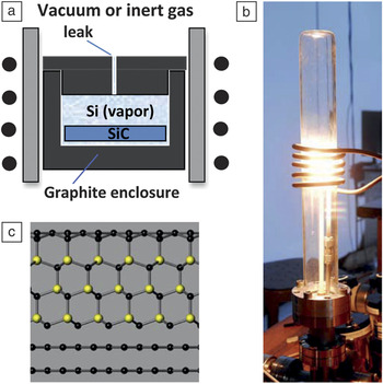
Because of the scalability of graphene nanostructuring and the structural quality of graphene nanostructures on the insulating SiC substrate, epitaxial graphene is recognized as an ideal platform for electronicsReference Berger, Song, Li, Li, Ogbazghi, Feng, Dai, Marchenkov, Conrad, First and de Heer9, Reference de Heer, Berger, Wu, First, Conrad, Li, Li, Sprinkle, Hass, Sadowski, Potemski and Martinez13, Reference de Heer, Berger, Ruan, Sprinkle, Li, Hu, Zhang, Hankinson and Conrad17–Reference Seyller, Bostwick, Emtsev, Horn, Ley, McChesney, Ohta, Riley, Rotenberg and Speck24 (see also the article in this issue by Nyakiti et al.). Epitaxial graphene sheets are produced by thermal decomposition of SiC at high temperature in a vacuumReference Forbeaux, Themlin and Debever25, Reference Van Bommel, Crombeen and Van Tooren26 or in argon gasReference Emtsev, Bostwick, Horn, Jobst, Kellogg, Ley, McChesney, Ohta, Reshanov, Rohrl, Rotenberg, Schmid, Waldmann, Weber and Seyller20 or by the confinement controlled sublimation (CCS) growth method.Reference de Heer, Berger, Ruan, Sprinkle, Li, Hu, Zhang, Hankinson and Conrad17 The highest-quality (single or multiple) graphene layers are grown in a near-equilibrium environment as in the CCS method. In the CCS growth technique (used in our graphene laboratories at Georgia Institute of Technology since 2003), a SiC chip is held in a graphite enclosure that is heated in a vacuum and supplied with a small leak (Figure 1a–b). The rate of graphene growth is controlled by the rate at which sublimed silicon vapor escapes through the leak. The graphene produced by CCS is superior in homogeneity to that obtained using methods that are far from equilibrium (for example, sublimation in a vacuum).Reference Forbeaux, Themlin and Debever25
Graphene growth by the confinement controlled sublimation (CCS) method. (a) A SiC chip is placed in a graphite enclosure that is provided with a small leak and inductively heated using a molybdenum sleeve as the susceptor. A quasi-equilibrium is established at high temperatures to moderate the graphene growth. (b) Photograph of the furnace showing the evacuated glass tube, the water-cooled radio-frequency induction coil, and the white-hot susceptor. (c) Schematic of graphene on SiC (silicon, yellow; carbon, black). The SiC wafer is shown as unrealistically thin to allow comparison of the two nonequivalent faces. The bottom face (C face) is covered with two graphene layers, whereas the top face (Si face) schematically terminates in a covalently bonded buffer layer. In subsequent growth on this face, the buffer layer is converted into a graphene layer by the new buffer layer that grows under it. Adapted from Reference Reference de Heer, Berger, Ruan, Sprinkle, Li, Hu, Zhang, Hankinson and Conrad17.

For electronics, epitaxial graphene on SiC has clear advantages over graphene deposited on substrates.Reference Hass, Feng, Li, Li, Zong, de Heer, First, Conrad, Jeffrey and Berger21, Reference Seyller, Bostwick, Emtsev, Horn, Ley, McChesney, Ohta, Riley, Rotenberg and Speck24, Reference de Heer27, Reference Sprinkle, Soukiassian, de Heer, Berger and Conrad28 First, it is grown directly on an insulating substrate, so it does not need to be transferred to another dielectric substrate; hence, it can be patterned immediately. In addition, the interface between epitaxial graphene and the silicon carbide substrate is formed at temperatures in excess of 1500°C, so that it is reproducible, ordered, and clean. Consequently, no water or impurities are trapped under the graphene. In contrast, transferred graphene produced by mechanical or chemical exfoliation or growth on metals is plagued by interface impurities. Moreover, graphene–SiC interfaces can be modified by passivation and intercalation. A further advantage is that the SiC substrate is a large-bandgap semiconductor already used in electronics applications. Monocrystalline wafers with diameters up to 100 mm and atomically smooth surfaces that are ready for epitaxial growth are readily available (at a price of about US$20/cm2).
Beyond applications, epitaxial graphene is ready for interrogation by the vast array of surface-science probes that are now available, most of which cannot be used on deposited graphene materials. A few examples are given in the remainder of this section. Other examples are included in the article in this issue by Conrad and Hicks.
Graphene can be epitaxially grown on either of the two polar faces of SiCReference Van Bommel, Crombeen and Van Tooren26 (see Figure 1c). On the (0001) silicon-terminated face of hexagonal 4H- or 6H-SiC, thin graphite composed of one or several graphene layers (ABA- or ABC-stacked) can be grown. A graphene-like nonconducting buffer layer sits next to the SiC substrate and forms a noninteracting interface with the graphene layer(s) on top of it.Reference Forbeaux, Themlin and Debever25, Reference Emtsev, Speck, Seyller, Ley and Riley29–Reference Varchon, Feng, Hass, Li, Ngoc Nguyen, Naud, Mallet, Veuillen, Berger, Conrad and Magaud31 Consequently, a Si-face monolayer is electronically essentially identical to a freestanding graphene layer.
Graphene grown on the (000 $\bar 1$) carbon-terminated face (the C face) of SiC is quite different from that grown on the (0001) Si face.Reference First, de Heer, Seyller, Berger, Stroscio and Moon18, Reference Kedzierski, Hsu, Healey, Wyatt, Keast, Sprinkle, Berger and de Heer19, Reference Berger, Song, Li, Wu, Brown, Naud, Mayou, Li, Hass, Marchenkov, Conrad, First and de Heer32 The CCS-grown layer stack on the C face is called multilayer epitaxial graphene (MEG) because it is azimuthally ordered in a particular way with alternating 0° and 30° rotations relative to the SiC(000
 $\bar 1$) substrate (although defects in this order are still abundant). Because of this non-Bernal stacking, the symmetry between the atoms in the unit cell is not broken in multilayers of C-face graphene.Reference Kedzierski, Hsu, Healey, Wyatt, Keast, Sprinkle, Berger and de Heer19, Reference Hass, de Heer and Conrad33 Consequently, even though it is multilayered, MEG has the electronic band structure of isolated graphene layers, with only a small perturbation due to weak effective interlayer coupling. Specifically, angle-resolved photoemission spectroscopy (ARPES) measurements showed a set of nearly independent linearly dispersing bands (Dirac cones) at the graphene K point, each one originating from an individual rotated layer in the multilayer stack.Reference Sprinkle, Siegel, Hu, Hicks, Tejeda, Taleb-Ibrahimi, Le Fevre, Bertran, Vizzini, Enriquez, Chiang, Soukiassian, Berger, de Heer, Lanzara and Conrad34 Experiments detected neither van Hove singularities at the K point, indicative of saddle points in the band structure, nor significant changes in the Fermi velocity,Reference Hicks, Sprinkle, Shepperd, Wang, Tejeda, Taleb-Ibrahimi, Bertran, Le Fèvre, de Heer, Berger and Conrad35 both of which had been predicted for rotated layers (also see the article in this issue by Hicks and Conrad).
Consequently, MEG films are stacks of graphene layers with the electronic structure of electronically decoupled graphene layers. The properties of this material have been extensively studied. For example, ongoing ARPES studies are being used to interrogate the subtle interactions between the topmost layers.Reference Sprinkle, Siegel, Hu, Hicks, Tejeda, Taleb-Ibrahimi, Le Fevre, Bertran, Vizzini, Enriquez, Chiang, Soukiassian, Berger, de Heer, Lanzara and Conrad34, Reference Hicks, Sprinkle, Shepperd, Wang, Tejeda, Taleb-Ibrahimi, Bertran, Le Fèvre, de Heer, Berger and Conrad35 Infrared Landau-level spectroscopy,Reference Orlita, Faugeras, Plochocka, Neugebauer, Martinez, Maude, Barra, Sprinkle, Berger, de Heer and Potemski36, Reference Sadowski, Martinez, Potemski, Berger and de Heer37 which probes transitions between Landau levels in a magnetic field, accesses interior layers in multilayer stacks, and Raman spectroscopyReference Faugeras, Nerriere, Potemski, Mahmood, Dujardin, Berger and de Heer38 provides information on electron–phonon coupling. Ultrafast optical-pump terahertz-probe spectroscopy monitors carrier relaxation processes.Reference Sun, Divin, Rioux, Sipe, Berger, de Heer, First and Norris39–Reference Winnerl, Orlita, Plochocka, Kossacki, Potemski, Winzer, Malic, Knorr, Sprinkle, Berger, de Heer, Schneider and Helm42
It is known that at least the topmost graphene layer on a C-face graphene stack is continuous over the entire wafer and atomically flat over hundreds of square micrometers.Reference Miller, Kubista, Rutter, Ruan, de Heer, First and Stroscio43 This allows high-resolution scanning tunneling microscopy (STM) experiments to be performed that are virtually impossible with deposited graphene layers, which need to be precisely located and contacted to a metallic drain and are plagued with electron–hole puddles and ripples that blur the spectral resolution. STM experiments on epitaxial graphene at millikelvin temperatures in high magnetic fields have provided, for instance, significant insight into the Landau-level distribution and a first-time direct mapping of the quantized states in graphene, with direct evidence of new many-body states in graphene.Reference Miller, Kubista, Rutter, Ruan, de Heer, First and Stroscio43–Reference Song, Otte, Kuk, Hu, Torrance, First, de Heer, Min, Adam, Stiles, MacDonald and Stroscio45
Epitaxial graphene films are well suited for chemical modification, by virtue of their large surface areas and unreactive and stable substrate. For example, MEG films have been successfully functionalized directly on the chip, to produce semiconducting graphene oxide films on the SiC substrate.Reference Wu, Sprinkle, Li, Ming, Berger and de Heer46 Aryl groups have been grafted onto MEG to modify its properties in attempts to produce high-mobility semiconducting graphene.Reference Niyogi, Bekyarova, Hong, Khizroev, Berger, de Heer and Haddon22, Reference Bekyarova, Itkis, Ramesh, Berger, Sprinkle, de Heer and Haddon47
Micropatterning by local thermal desorption of epoxy and hydroxyl groups has been proposed as a method to create conducting nanoribbons on a nonconducting epitaxial graphene oxide matrix.Reference Wei, Wang, Kim, Kim, Hu, Yakes, Laracuente, Dai, Marder, Berger, King, de Heer, Sheehan and Riedo48, Reference Kim, Zhou, Hu, Acik, Chabal, Berger, de Heer, Bongiorno and Riedo49 Noncovalent chemical modifications of epitaxial graphene that preserve the electronic band structure of graphene were also successfully achieved for protein immobilization.Reference Kodali, Scrimgeour, Kim, Hankinson, Carroll, de Heer, Berger and Curtis50
Electronic transport and devices on the C face
Quantum Hall effect on an epitaxial monolayer
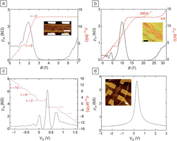
One distinctive characteristic of graphene is an additional quantum number that represents the weight of the wave function for a particular momentum direction on each of the two triangular sublattices that compose the honeycomb atomic structure. This quantum number, called pseudospin, has the characteristics of a spin but is bound to the direction of momentum. Because the electronic wave character (pseudospin) cannot be changed by scattering in the perfect atomic structure, the dynamics of the electrons is modified compared to that of classical two-dimensional electron gases. In particular, the presence of a pseudospin causes two-dimensional graphene to be immune from back-scattering, increasing carrier mobility.Reference Katsnelson7 It also manifests in the appearance of quantum Hall effect (QHE) plateaus at conductance values that are half-integer multiples of 4e 2/h.Reference Zhang, Tan, Stormer and Kim51, Reference Novoselov, Geim, Morozov, Jiang, Katsnelson, Grigorieva, Dubonos and Firsov52 (Here, e is the electron charge, and h is Planck’s constant. The factor of four multiplying e 2/h is expected because of the twofold valley and twofold spin degeneracies in graphene.) The half-integer QHE, hallmark of monolayer graphene, is clearly observed in monolayer epitaxial graphene grown on the C faceReference Hu, Ruan, Guo, Dong, Palmer, Hankinson, Berger and de Heer10, Reference Wu, Hu, Ruan, Madiomanana, Hankinson, Sprinkle, Berger and de Heer53, Reference de Heer, Berger, Wu, Hu, Ruan, Stroscio, First, Haddon, Piot, Faugeras and Potemski54 (Figure 2).
The quantum Hall effect in C-face epitaxial monolayer graphene for micrometer-wide Hall samples with CCS-produced graphene. Resistivity ρxx (black) and Hall resistance ρxy (red) versus magnetic field at 4 K for (a) the C-face Hall bar shown in the inset (mobility μ = 39,800 cm2 V–1 s–1, charge density n = 0.19 × 1012 cm–2) and (b) the C-face Hall bar shown in the inset (μ = 21,100 cm2 V–1 s–1, n = 0.92 × 1012 cm–2), also showing the persistence of the ν = 2 plateau in ρxy at 200 K (where ν represents the filling factor). (c) Resistivity ρxx and Hall conductivity σxy = ρxy/(ρxx 2 + ρxy 2) versus gate voltage V G for a top-gated C-face Hall bar (1 μm × 4.3 μm), showing plateaus in the n- and p-doped regimes. The mobility for n doping is 6200 cm V–1 s–1, and that for p doping is 8500 cm V–1 s–1. The application of the top gate significantly reduces the mobility compared with those of the bare samples in (a) and (b). (d) Resistivity ρxx as a function of gate voltage at 4 K and zero magnetic field. The inset shows the Hall bar measured in (c) and (d). All scale bars are 2 μm. Adapted from References 10, 53, and 54.

The charge density in an epitaxial graphene monolayer can be adjusted by compensating the intrinsic n doping through exposure to the environment (water, light) or through resist coating, or it can be tuned by a top gate, as in Figure 2c–d.Reference Hu, Ruan, Guo, Dong, Palmer, Hankinson, Berger and de Heer10 When graphene is environmentally doped, heating it in a vacuum restores its pristine condition. Mobilities up to 40,000 cm2 V–1 s–1 can be achieved at a carrier density of 0.19 × 1012 cm–2, which is low enough for observation of the extended Rxy = h/2e 2 plateau (corresponding to a filling factor [the electron density relative to the number of states of a Landau level] of ν = 2) at a relatively low magnetic field (onset at B ≈ 3 T).Reference Hu, Ruan, Guo, Dong, Palmer, Hankinson, Berger and de Heer10 Note also that a well-defined plateau is observed in Figure 2b at temperatures above 77 K, that is, well above the usual temperature for quantization in conventional two-dimensional electron gases.Reference de Heer, Berger, Wu, Hu, Ruan, Stroscio, First, Haddon, Piot, Faugeras and Potemski54 This opens the way to QHE-based metrology applications (see the article in this issue by Schopfer and Poirier).
Ultrahigh-frequency field-effect transistors
At the time of this writing, graphene is not suited for digital electronics, because of its lack of a bandgap, which is absolutely required for digital switches. However, for the channel material of field-effect transistors (FETs) in amplifiers, a bandgap is not required, so graphene provides a unique opportunity for ultrahigh-frequency electronics. These devices require (among other properties) a high-mobility channel material. Moreover, a silicon carbide substrate is compatible with these high frequencies.
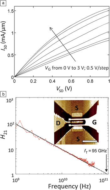
Several proof-of-concept experiments have demonstrated the feasibility of this technology.Reference Kedzierski, Hsu, Healey, Wyatt, Keast, Sprinkle, Berger and de Heer19, Reference Moon, Curtis, Hu, Wong, McGuire, Campbell, Jernigan, Tedesco, VanMil, Myers-Ward, Eddy and Gaskill55, Reference Lin, Valdes-Garcia, Han, Farmer, Meric, Sun, Wu, Dimitrakopoulos, Grill, Avouris and Jenkins56 A unity-current-gain cutoff frequency of f T > 200 GHz has been demonstrated with a Si-face epitaxial graphene channel device, thereby showing that this material can indeed be used for state-of-the-art electronic devices.Reference Lin, Farmer, Jenkins, Wu, Tedesco, Myers-Ward, Eddy, Gaskill, Dimitrakopoulos and Avouris57 Rapid progress is also being made with C-face graphene FETs (see Figure 3), for which f T ≈ 100 GHz is routinely obtained. To achieve such performance, a double-gate structure covering a short and wide channel between the source and drain is used (Figure 3b inset). This transistor design has been optimized to minimize parasitic capacitances. The device is top-gated with an aluminum-capped Al2O3 dielectric that preserves good electronic mobility of 8700 cm2 V−1 s−1. As usual for graphene devices, the desirable saturation of the current with increasing source–drain voltage is not reached (Figure 3a).Reference Lin, Farmer, Jenkins, Wu, Tedesco, Myers-Ward, Eddy, Gaskill, Dimitrakopoulos and Avouris57 Nonetheless, the device exhibits promising characteristics (maximum current density greater than 1.5 mA μm–1 and transconductance greater than 0.4 mS μm–1 at a charge density of n = 1.6 × 1012 cm−2). (For further discussion of transistor characteristics, see the article in this issue by Avouris and Xia.)
Ultrahigh-frequency C-face epitaxial graphene field-effect transistor (GFET). (a) Source–drain current density (I SD) versus voltage (V SD) on a 200-nm-long gate, 3-μm-wide device at gate voltages (V G) from 0 V to 3 V in 0.5-V steps. A current density greater than 1.5 mA/μm can be applied to the device, and mild current saturation is observed at large drain–source biases. (b) ac current gain (H 21) versus frequency for the GFET in (a) after de-embedding. A cutoff frequency (f T) of 90 GHz is extracted by extrapolating the measurement to unity gain. Inset: Atomic force microscopy (AFM) image of a dual-gate GFET similar to the one measured in (a) and (b). D, drain; G, gate; S, source. Scale bar = 5 μm. Adapted from Reference Reference Hu, Ruan, Guo, Dong, Palmer, Hankinson, Berger and de Heer10.

To be competitive with current semiconductor technology, the f T value of graphene devices will need to be increased considerably, as half-terahertz operation of SiGe heterojunction bipolar transistor has already been demonstrated.Reference Krithivasan, Lu, Cressler, Rieh, Khater, Ahlgren and Freeman58 Terahertz operation is, in principle, possible for epitaxial graphene, based on the high carrier velocity in graphene and the high phonon frequency of SiC.Reference Kim, Choi, Kim, Cho and Chung11, Reference Nienhaus, Kampen and Monch59 One of the most significant limitations is the access resistance, which is the series resistance of the short, ungated portion of graphene between the source and drain leads seen in the inset of Figure 3b. Even though the resistivity of graphene at room temperature is comparable to that of copper (10 μΩ cm), the resistance of a graphene source lead with a length-to-width aspect ratio of 10:1 is several kiloohms. The minimum reported access resistance of 350 Ω per micrometer of channel width is still prohibitive for terahertz operation, but this problem is primarily technical and surmountable using C-face graphene, which has a high carrier mobility.
Spintronics
Epitaxial graphene has also recently demonstrated its utility for spintronics. Spintronic devices use spin rather than charge as the state variable for information processing.Reference Wolf, Awschalom, Buhrman, Daughton, von Molnar, Roukes, Chtchelkanova and Treger60 The basic spin valve operates as follows: Spin-polarized electrons are injected into a graphene ribbon using a magnetically polarized contact. The spin polarization is detected by means of a second magnetically polarized contact, which preferentially admits electrons whose spin is aligned with it. The spin signal is the difference in the resistance between the cases of parallel and antiparallel magnetization of the electrodes.
Recently, highly efficient spin transport was measured in MEG with spin signals in the megaohm range, efficiencies up to 75%, and spin propagation lengths exceeding 100 μm.Reference Dlubak, Martin, Deranlot, Servet, Xavier, Mattana, Sprinkle, Berger, de Heer, Petroff, Anane, Seneor and Fert61 The high efficiency (the difference in the measured resistance between two oppositely magnetically polarized contacts, relative to perfect transmission) and long spin diffusion length imply an exceptionally small degradation of spin information during the transport through the epitaxial graphene channel. The spin diffusion lengths in graphene are nearly two orders of magnitude higher than those reported in metals, semiconductor systems, and transferred graphene flakes. Such exceptional results are attributable not only to the high mobility of epitaxial graphene, but also to the flatness of the layers and the absence of ripples that can depolarize the spins. Further, these promising results indicate that epitaxial graphene could serve as a scalable platform for spintronics in more complex structures. Although much more development is still needed, the possibility of spintronic devices and networks might now be a little closer thanks to graphene. (See the article in this issue by Seneor et al. for a detailed discussion of graphene use for spintronics.)
Structured graphene
Since the advent of graphene-based electronics,Reference Berger, Song, Li, Li, Ogbazghi, Feng, Dai, Marchenkov, Conrad, First and de Heer9 it has been clear that graphene’s potential as a superior electronic material is most relevant at the nanoscale, where quantum interference effects manifest themselves in structures on the order of the Fermi wavelength, λF. To gauge the relevant dimensions, note that, at a charge density of n s ≈ (2–5) × 1012 cm–2 (the natural charge of a pristine epitaxial graphene monolayer), that is, for a Fermi energy about 200 meV above the Dirac point, λF is approximately 20 nm. It becomes greater than 300 nm for the quasineutral graphene layers (n s < 5 × 109 cm–2) in the stack of MEG.
Whereas most schemes for fabricating nanoscale graphene structures start from extended graphene sheets and pattern them by lithographically defined etching, epitaxial graphene on SiC can be shaped directly at the nanoscale without such postgrowth patterning.Reference Hu, Ruan, Guo, Dong, Palmer, Hankinson, Berger and de Heer10, Reference Sprinkle, Ruan, Hu, Hankinson, Rubio-Roy, Zhang, Wu, Berger and de Heer12 Lithographically patterned graphene nanoribbons have been extensively studied. As described previously, the original ideaReference Berger, Song, Li, Li, Ogbazghi, Feng, Dai, Marchenkov, Conrad, First and de Heer9 was that graphene ribbons would be semiconductors with bandgaps on the order of 1 eV/W, where W is the ribbon width in nanometers. Several studies in fact appeared to confirm bandgaps of this order in patterned graphene ribbons.Reference Han, Özyilmaz, Zhang and Kim62 However, in most cases, the large response to the gate voltage in very narrow ribbons (with on/off current ratios up to 106) turned out to be caused by a mobility gap rather than a bandgap.Reference Oostinga, Sacepe, Craciun and Morpurgo63 The edges of lithographically patterned ribbons are disordered (electronically resembling a series of quantum dots). This disorder causes strong localization of the charge carriers and a large reduction in the mobility in the energy region near the Dirac point, degrading the current at low charge densities. Because the localized states still must be charged and discharged by the device currents, devices that rely on mobility gaps are typically not suitable for high-speed digital electronics.
Remedying this problem requires methods to keep the ribbon edges intact. The following subsections describe three paths that avoid lithographic patterning of graphene itself and instead produce the desired shapes in the graphene growth phase. The first method promotes graphene growth by etching depressions or mesas on SiCReference Sprinkle, Ruan, Hu, Hankinson, Rubio-Roy, Zhang, Wu, Berger and de Heer12 and is best suited for C-face graphene. The second approach, C-face patterning, uses a lithographically defined cap that prevents formation of graphene under it.Reference Rubio-Roy, Zaman, Hu, Berger, Moseley, Meindl and de Heer64 The third method is the most promising and consists of growing graphene on the faceted sidewalls of trenches that are etched into the SiC.Reference Hu, Ruan, Guo, Dong, Palmer, Hankinson, Berger and de Heer10, Reference Sprinkle, Ruan, Hu, Hankinson, Rubio-Roy, Zhang, Wu, Berger and de Heer12 This method takes advantage of the facet-dependent growth rate. Because Si-face graphene growth is particularly slow, the sidewalls of the trenches etched in SiC are the first to graphitize.
C-face pits and mesas
Monolayer graphene growth on the C face is complexReference de Heer, Berger, Ruan, Sprinkle, Li, Hu, Zhang, Hankinson and Conrad17, Reference Hicks, Shepperd, Wang and Conrad65 and ultimately yields a uniform distribution of monolayer patches over the silicon carbide substrate. High-mobility monolayer patches as large as several hundred square micrometers in area can be grown continuously over the substrate steps.Reference Hu, Ruan, Guo, Dong, Palmer, Hankinson, Berger and de Heer10 The CCS growth method is used, and growth is arrested after a few minutes at 1550°C. Monolayer C-face films are identified by atomic force microscopy (AFM), ellipsometry, optical transmission and Raman spectroscopies, and ultimately by the characteristic half-integer QHEReference Wu, Hu, Ruan, Madiomanana, Hankinson, Sprinkle, Berger and de Heer53 (see Figure 2). Note that growth at screw dislocations (which are always present in current SiC crystal wafers) is difficult to control and typically causes deep crevices covered with multilayer graphene.
Structured growth of monolayers on the C face has routinely been achieved on etched mesas and trenches in 4H-SiC.Reference Hu, Ruan, Guo, Dong, Palmer, Hankinson, Berger and de Heer10 Following Reference Reference Powell, Neudeck, Trunek, Beheim, Matus, Hoffman and Keys66, a good starting point for graphene growth is a surface with step-free mesas. These form under certain conditions when the natural steps originating from the substrate miscut angle flow at high temperature and bunch at the edges of etched mesas. Graphene on the C face is recognized by its pleats, which result from a larger contraction of SiC relative to graphene upon cooling from the high temperature applied during growth.Reference Hu, Ruan, Guo, Dong, Palmer, Hankinson, Berger and de Heer10
In another approach,Reference Hu, Ruan, Guo, Dong, Palmer, Hankinson, Berger and de Heer10 monolayer graphene growth at specific locations can also be initiated at the edges of trenches etched in SiC prior to graphitization. Further work will reveal whether this method can lead to a viable process for growing nanoscale graphene patches at predetermined locations.
Local capping
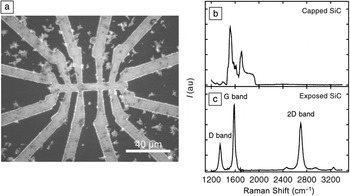
Another route for growing graphene at specific locations is to prevent silicon sublimation from the SiC substrate by capping it with an aluminum nitride layer.Reference Rubio-Roy, Zaman, Hu, Berger, Moseley, Meindl and de Heer64 The AlN coating is patterned and etched away to open bare SiC windows for subsequent graphitization by the CCS methodReference de Heer, Berger, Ruan, Sprinkle, Li, Hu, Zhang, Hankinson and Conrad17 (see Figure 4a). This process relies on the ability of the cap to withstand graphitization temperatures up to 1420°C under 100 Pa of argon pressure. The Raman spectra in Figure 4b–c clearly show that, under optimized growth conditions, the AlN coating efficiently prevents graphene growth under it.Reference Rubio-Roy, Zaman, Hu, Berger, Moseley, Meindl and de Heer64 Consequently, the resulting graphene structure does not need postgrowth etching. Graphene Hall bars were fabricated with this method and characterized by scanning Raman spectroscopy, ellipsometry, and transport measurements. The Hall mobility for the Hall bar in Figure 4a was determined to be about 600 cm2 V–1 s–1, and the mobility can be further enhanced for such structures by fine tuning the growth conditions and improving the quality of the SiC surface prior to graphitization.
Capping method for structured graphene growth using a patterned AlN cap. (a) AFM image of a completed graphene Hall bar structure fabricated by the CCS method. The light gray areas correspond to graphene, and the dark areas correspond to AlN-covered regions that prevent graphene growth. Metal contacts (gold/palladium) are applied for subsequent electrical measurements. This Hall bar has a Hall mobility of about 600 cm2 V–1 s–1, significantly less than that of pristine graphene. (b) Micro-Raman spectrum of the AlN-capped SiC substrate, which does not exhibit graphene features after CCS annealing. (c) Micro-Raman spectrum of the graphene areas, showing characteristic graphene features (D, G, and 2D bands). The relatively intense D band confirms that the graphene is significantly disordered, accounting for the observed low mobilities. Adapted from Reference Reference Rubio-Roy, Zaman, Hu, Berger, Moseley, Meindl and de Heer64.

Sidewalls
The third, extremely promising, route for graphene growth is the structured growth methodReference Hu, Ruan, Guo, Dong, Palmer, Hankinson, Berger and de Heer10, Reference Sprinkle, Ruan, Hu, Hankinson, Rubio-Roy, Zhang, Wu, Berger and de Heer12 (also called the templated growth method), in which graphene growth is initiated on the sidewalls of pre-etched SiC trenches. This process relies on the observations that graphene growth is slowest on the (0001) face and that growth on this face proceeds from the steps to the terrace regions.Reference Norimatsu and Kusunoki67
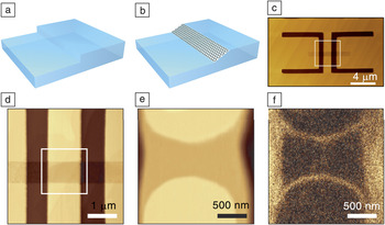
The general approach is schematically depicted in Figure 5a–c; details can be found in References 12 and 17. The SiC surface (Si face) is first vertically plasma etched through a patterned mask to produce steps of well-defined height. When required, this procedure is repeated several times to produce structures with varying depths (as shown in Figure 5c). The etched SiC template is then annealed at a temperature of about 1550°C for about 10 min, and the etched steps crystallize at high temperature toward equilibrium (1 $\bar 1$0n) or (11
 $\bar 2$n) facets. For trenches on the order of 10 nm in depth, the normals to the facet surfaces have angles of 28–32° with respect to the (0001) direction.
Illustrative example of structured growth patterning. (a)–(c) Schematic illustration of the production of structured graphene and devices: (a) A vertical step is etched in the SiC substrate. (b) After CCS growth, the sidewall has recrystallized into a stable SiC facet, on which graphene grows preferentially. (c) Repeated plasma etching produces structures with varying depths. (d–f) A graphene ribbon is seamlessly connected to wide graphene leads. (d) AFM image of a SiC surface patterned with two deep U-shaped etched trenches (dark lines) connected to a shallow trench for subsequent graphene nanoribbon growth. Four wide graphene leads form at the edges of the two deep trenches. These form electrical leads connected to two thin graphene ribbons that form on the upper and lower edges of the shallower trench (faint horizontal stripe). (e) AFM image, representing the topography, and (f) electrostatic force microscopy (EFM) image, whose contrast distinguishes graphene from silicon carbide, of the surface presented in (d) after CCS graphitization. The rounding comes from the SiC step flow to produce a stable crystalline SiC facet. Adapted from References 10 and 12.

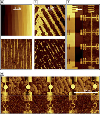
Using the CCS growth process with controlled growth parameters (time and temperature), a monolayer graphene film can be produced on only these facets and not (or minimally) on the (0001) upper and lower surfaces. The facets, or sidewalls, can be shaped into narrow ribbons, rings, crosses, or essentially any shape. Notably, for transport measurements, graphene nanoribbons can be seamlessly connected to four wide ribbons for four-point transport measurements (Figure 5d–f). For this purpose, a shallow (∼10-nm) trench is etched, bridging two previously etched deep U-shaped trenches (>100 nm, see Figure 5d).Reference Hu, Ruan, Guo, Dong, Palmer, Hankinson, Berger and de Heer10 After CCS growth, the sidewalls of the U trenches form the broad graphene leads for the two narrow graphene sidewall ribbons between the U’s (Figure 5e–f). Metal contacts are provided to the wide graphene leads for transport measurements of the narrow graphene ribbons. Gate structures can be subsequently patterned on top of the sidewall ribbon. Further examples of structured graphene are shown in Figure 6.
Examples of epitaxial graphene sidewall structures produced by the structured growth method, demonstrating its versatility: (a) an array of parallel ribbons grown on the step edges of a vicinal surface, (b) graphene grown in many orientations on the sidewalls of complex convoluted trenches, (c) a Hall bar with four transverse voltage probes, and (d) rings grown on the sidewalls of pillars. The top images in (a), (b), and (d) and the left image in (c) represent the AFM topography, and the corresponding bottom and right images are EFM images showing bright areas where graphene grows at the edges of the etched patterns. Adapted from Reference Reference Hu, Ruan, Guo, Dong, Palmer, Hankinson, Berger and de Heer10.

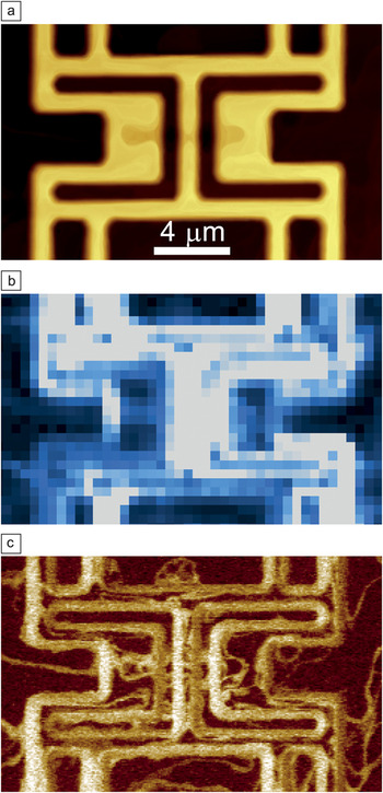
The structured growth method circumvents the damaging lithographic patterning process that causes large mobility reductions in lithographically patterned graphene ribbons. Instead of being chemically etched by oxygen plasma through a mask (which is far from gentle), the graphene edges of ribbons produced by structured growth are annealed at high temperature and anchored into the reconstructed SiC surface. Graphene nanostructures can be imaged by electrostatic force microscopy (EFM) at high resolution (about 10 nm according to modeling of the tip–graphene interaction). Raman spectroscopy (about 1-μm resolution) unambiguously shows the characteristic graphene spectrum (similar to that in Figure 4b). In particular, for graphene grown on the structure shown by AFM in Figure 7a, spatial scans of the graphene Raman 2D peak (Figure 7b) reveal that, in well-prepared samples, graphene grows almost exclusively on the sidewalls, as confirmed by EFM (Figure 7c).
(a) AFM image, (b) Raman 2D peak mapping, and (c) EFM image of a Si-face SiC surface with graphene selectively grown on the sidewalls, confirming that graphene growth is largely confined to the sidewalls.

All graphene ribbons produced by this method have been found to be metallic with significant mean free paths. There is no evidence for a bandgap or a transport gap, in contrast to lithographically patterned graphene.Reference Han, Özyilmaz, Zhang and Kim62, Reference Oostinga, Sacepe, Craciun and Morpurgo63, Reference Özyilmaz, Jarillo-Herrero, Efetov and Kim68 The absence of localization or a Coulomb blockade, which is observed when tunneling occurs between small decoupled graphene regions,Reference Oostinga, Sacepe, Craciun and Morpurgo63 indicates much-reduced scattering compared to that of nanoribbons etched after growth, presumably due to smoother edges. In fact, early tight-binding calculationsReference Nakada, Fujita, Dresselhaus and Dresselhaus14 predicted that all graphene ribbons should be metallic, with the exception of those with armchair edges. Even among armchair ribbons, only those for which the width is an integer multiple of three hexagons are semiconductors. Several calculations that go beyond the tight-binding approximationReference Son, Cohen and Louie69, Reference Hassan70 have predicted that ribbons will be semiconductors, but in all cases, the edge structure and chemistry play essential roles, and their control is important.
High-resolution transmission electron microscopy cross sections and scanning tunneling microscopy images of graphene grown on the sidewalls of steps indicate that graphene curves terminate perpendicular to the silicon carbide surface at the bottom of steps and that the graphene edges are mainly of the zigzag variety.Reference Norimatsu and Kusunoki67
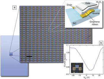
The sidewall graphitization method is also appropriate for large-scale production of patterned structures (see examples in Figure 6). Ribbons and interconnecting structures can be produced simultaneously, after the SiC substrate has been structured by plasma etching. Note that the graphene nanoribbon width is determined by the step height (and thus the SiC plasma etch time) and not by the feature size of the SiC etch mask. Hence, optical lithography can be used to produce nanometric wafer-scale graphene devices. An example of 10,000 interconnected transistors produced on a 4 mm × 6 mm SiC chip is shown in Figure 8, along with some transport characteristics.Reference Sprinkle, Ruan, Hu, Hankinson, Rubio-Roy, Zhang, Wu, Berger and de Heer12 Wide graphene ribbons (about 250 nm in width) were produced in this array on the C face, demonstrating the feasibility of sidewall growth on both faces. The weak gating is attributed to the metallic nature of the ribbons.
Example of large-scale patterning of epitaxial graphene devices using the structured growth method. (a) Illustration of 10,000 transistors fabricated within a 4 mm × 6 mm chip using the sidewall graphitization method, with a schematic of the transistor structure at the top right. (b) Typical gating characteristics between source S and drain D showing the conductance G (in millisiemen-squares) versus gate voltage V G. Inset: Plan view of the transistor structure. Scale bar, 20 μm; channel length, 7 μm. Adapted from Reference Reference Sprinkle, Ruan, Hu, Hankinson, Rubio-Roy, Zhang, Wu, Berger and de Heer12.

Conclusions
This overview of epitaxial graphene for electronics applications is meant to stimulate further attention to this field. Our perspective is that, for graphene to have an impact on electronics, the basic tenets of microelectronics should be respected. Modern microelectronics deals with structures that are a few tens of nanometers in size that are reliably patterned by the billions. The only reason that this can be achieved is that the silicon substrates being used are atomically well-defined: they are single crystals, which is obviously preferable over disordered substrates. Consequently, it is very likely that any new electronics technology will adopt this strategy from the outset.
Herein, we have shown that graphene on single-crystal silicon carbide offers a wide range of advantages. Beyond its potential for large-scale patterning, epitaxial graphene on SiC can be studied using state-of-the-art surface-science probes, including angle-resolved photoemission spectroscopy, low-energy electron diffraction , scanning tunneling microscopy, atomic force microscopy, transmission electron microscopy, and many others, that cannot be used for materials produced on poorly defined substrates. It is clear that epitaxial graphene electronics has not yet realized its full potential. However, the first small steps have been made. Commercially viable ultrahigh-frequency epitaxial graphene analog devices are on the horizon. The most critical next step will be to open a bandgap in the material, and steady progress is being made to achieve this goal. Indeed, epitaxial graphene has few competitors in efforts to produce new electronics platforms.
Acknowledgments
We acknowledge funding from the National Science Foundation (DMR-0820382), the Keck Foundation, the Air Force Office of Scientific Research, and the Partner University Fund. We warmly thank P. S. Chakraborty, N. Lourenco, and J. Cressler for the ultrahigh-frequency FET measurements presented in Figure 3.