Introduction
Flexible electrode is an essential component of various recently emerging portable, flexible, and wearable electronic devices such as flexible energy storage devices, flexible displays, wearable sensor system, and implantable medical devices [Reference Jia, Jiang, Zheng, Tan, Cao, Liu, Yue, Sun and Liu1, Reference Yu, Luo, Wu, Jiang, Li, Fan, Li and Wang2, Reference Zhu, Zheng, Wang, Zheng, Fang, Zhu, Yu, Tong and Lu3, Reference Yao, Chen, Xu, Zeng, Yang, Ye, Liu, Wu and Yu4, Reference Liang, Chang, Kuo, Cho, Jiang, Jhuang, Rwei and Borsali5, Reference Song, Fang, Li, Xu, Zhang, Han, Shan and Zeng6, Reference Park, Kim, Kang, Shim, Woo, Kim and Choi7, Reference Jo, Kwon, Kim, Park, An, Yarin and Yoon8, Reference Yetisen, Martinez-Hurtado, Ünal, Khademhosseini and Butt9, Reference Huynh and Haick10, Reference Pu, Tu, Han, Zhang, Wu, Fang, Wu, Zhang, Yu and Li11]. In many cases, the major limitation for the development flexible electrode materials with superior performance is their long-term service reliability since the flexible devices are inevitably subjected to cyclic stretching, repeatedly bending, or even twisting in their daily use. One effective solution is to utilize robust materials for optimizing their performance and long-term service reliability [Reference Hwang, Kim, Kim, Lee, Lim, Kim, Oh, Ryu and Han12].
Recently, carbon nanotubes (CNT) [Reference Park, Vosguerichian and Bao13, Reference Liu, Ding, Zhong, Han, Wang, Meng, Qiu, Zhang, Peng and Zhang14, Reference Zhang, Xiang, Yang, Xiao, Han, Ding, Zhang, Hu and Peng15], reduced graphene oxide (rGO) [Reference Li, Ding, Zhang, Qiao and Liu16, Reference Chong, Xiao, Huang, Yao, Cui, Qin, Gao and Kim17], carbon cloth [Reference Deng, Jiang, Hu, Liu, Zhang, Liu and Li18, Reference Guan, Sumboja, Wu, Ren, Liu, Zhang, Liu, Cheng, Pennycook and Wang19, Reference Liu, Zhang, Wang, Chen, Chen, Zhou and Shen20], conductive paper (cellulose) [Reference Zhang, Zhang, Cui, Ge, Cheng, Yan, Yu and Liu21, Reference Yang, Huang, Payne, Sun and Wang22], low-dimensional nanostructured transition metal dichalcogenides [Reference Park, Kim, Kang, Shim, Woo, Kim and Choi7, Reference Yu, Fu, Zeng, Lin, Yan, Lai, Tang, Suenaga, Zhang and Liu23] and ultrathin metal films [Reference Luo, Zhu and Zhang24, Reference Wan, Luo, Li, Liu and Zhang25, Reference Zhang, Xiao, Luo, Zhu and Zhang26, Reference Yun27], as well as their composites [Reference Wimalananda, Kim and Lee28, Reference Tseng, Chen, Ulaganathan, Lee, Chiang, Chang and Chen29, Reference Hwang, Song, Han, Bae, Song, Choi, Park and Song30, Reference Wang, Li, Liu, Feng, Wang, Yang, Zhang, Zhu and Zhang31] have been utilized to replace the conventional indium tin oxide (ITO) material, which is so brittle that not suitable for the flexible electrodes [Reference Kumar and Zhou32]. Due to the large contact resistance of tube–tube junctions, a CNT network is still far from practical applications [Reference Yun27]. One of the potential alternatives is metal (i.e., Au, Ag, and Cu)-based nanostructures in the form of either a ultrathin continuous film (dozens or hundreds of nanometer thickness) or a nanowire network supported by flexible polymer substrates [Reference Yun27, Reference Wang, Hassan, Liu and Yu33]. Ultrathin Cu film is one of the most widely used metallic interconnect/electrodes in the devices due to its relatively low cost and high electrical conductivity. The yield strength of the Cu film was improved by 1000 MPa, from ∼300 to ∼1300 MPa, by tailoring microstructure, such as the film thickness and the grain size [Reference Zhang, Sun, Zhang, Gong, Sun and Wang34]. In addition, fatigue cracking resistance was enhanced to some extent by annealing but still not fully satisfied [Reference Zhang, Xiao, Luo, Zhu and Zhang26, Reference Zhang, Volkert, Schwaiger, Wellner, Arzt and Kraft35]. A key question is how to further improve the long-term mechanical reliability and stability without loss of electrical conductivity. Liu et al. found that the layer interface of laminated composites can delay the premature of local necking of the constituent layers, resulting in a significant enhancement in the tensile ductility [Reference Liu, Zhang and Zhang36]. Therefore, one of the possible approaches to fabricate ultrathin metal films with high-fatigue performance is to strongly constrain and delay the formation of fatigue damage of the metal film by introducing a heterogeneous interface.
Graphene with a honeycomb lattice, that combines remarkable mechanical properties (yield strength is 130 GPa and Young’s modulus is 1 TPa), high electrical conductivity [the electron mobility is 2 × 105 cm2/(V s) and the minimum sheet resistance of an ideal undoped monolayer graphene is 31 Ω/sq.], and thermal conductivity (∼5300 W/m K), is a unique electrode material as well [Reference Hwang, Kim, Kim, Lee, Lim, Kim, Oh, Ryu and Han12, Reference Lee, Wei, Kysar and Hone37, Reference Kim, Lee, Yeom, Shin, Kim, Cui, Kysar, Hone, Jung, Jeon and Han38, Reference Song, Park, Kim, Choi, Jun, Lee, Kong, Paik and Jeon39]. In particular, the integration of graphene and ultrathin metal film enables the mechanical properties of the graphene/metal composites largely improved without loss of electrical conductivity [Reference Kim, Shin, Choi, Rho, Park, Moon, Kim, Lee, Lee, Kim, Lee, Kim, Hong and Bae40, Reference Cao, Xiong, Tan, Ji, Amin-Ahmadi, Guo, Fan, Guo, Li and Zhang41, Reference Hwang, Yoon, Jin, Lee, Kim, Hong and Jeon42, Reference Yang, Wang, Shi, Wang, Cui, Wei, Xu, Zhu and Fei43, Reference Jiang, Zhou and Liu44, Reference Chen, Ying, Wang, Du, Liu and Huang45, Reference Tang, Yang, Wang and Li46, Reference Kim, Lee and Han47]. Therefore, considerable amount of research has been conducted on fabrication the graphene/metal composites, including electrodeposition [Reference Kim, Shin, Choi, Rho, Park, Moon, Kim, Lee, Lee, Kim, Lee, Kim, Hong and Bae40, Reference Ren, Meng, Shehzad, Xu, Qu, Yu and Luo48], molecule-level mixing [Reference Hwang, Yoon, Jin, Lee, Kim, Hong and Jeon42, Reference Yang, Wang, Shi, Wang, Cui, Wei, Xu, Zhu and Fei43, Reference Chen, Ying, Wang, Du, Liu and Huang45], ball milling [Reference Kim, Lee and Han47, Reference Wang, Li, Fan, Pan, Chen and Zhang49, Reference Li, Fan, Tan, Guo, Xiong, Su, Li and Zhang50] followed by spark plasma sintering [Reference Hwang, Yoon, Jin, Lee, Kim, Hong and Jeon42, Reference Yang, Wang, Shi, Wang, Cui, Wei, Xu, Zhu and Fei43, Reference Jiang, Zhou and Liu44, Reference Chen, Ying, Wang, Du, Liu and Huang45, Reference Tang, Yang, Wang and Li46] and/or high-ratio differential speed rolling [Reference Kim, Lee and Han47], and hot-pressing [Reference Cao, Xiong, Tan, Ji, Amin-Ahmadi, Guo, Fan, Guo, Li and Zhang41] after chemical vapor deposition (CVD) methods. Several technical challenges such as controlling the layer numbers and the quality of rGO mixed in the composites are critical during the fabrication process. Due to extreme high temperature (∼1000 °C) during the CVD process, large-area and high-quality monolayer or multilayer graphene needs to be firstly grown on Cu foils and then transferred onto the Cu/PI by wet etching transfer technique [Reference Li, Cai, An, Kim, Nah, Yang, Piner, Velamakanni, Jung, Tutuc, Banerjee, Colombo and Ruoff51], which paves a road for fabricating flexible metal electrode coated with controllable layers of graphene [Reference Hwang, Kim, Kim, Lee, Lim, Kim, Oh, Ryu and Han12, Reference Kim, Lee, Yeom, Shin, Kim, Cui, Kysar, Hone, Jung, Jeon and Han38]. So far, the durability of these flexible devices is only calculated by measuring the electrical resistivity or resistance evolution after the electrode was bent at a certain curvature for 103–106 cycles [Reference Hwang, Kim, Kim, Lee, Lim, Kim, Oh, Ryu and Han12, Reference Tseng, Chen, Ulaganathan, Lee, Chiang, Chang and Chen29]. In fact, cracks may initiate as the electrical resistance imperceptibly increases and then gradually propagate with fatigue cycle increasing. Thus, the critical strain amplitude for fatigue crack initiation needs to be determined. What is more, to further improve the mechanical reliability of the flexible electrodes under cyclic loading, the mechanism for the graphene delaying the fatigue damage formation of covered metal films is urgently needs to be clarified.
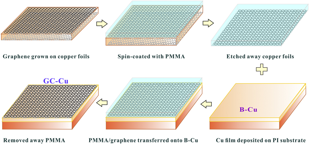
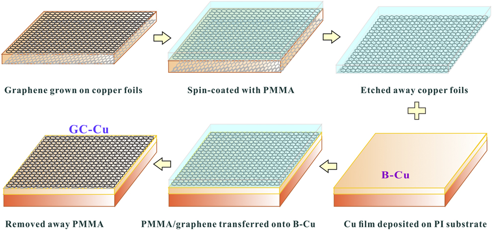
In this work, we fabricated a graphene-covered Cu (GC-Cu) composite electrode with a thickness of 100 nm on a polyimide (PI) substrate by means of a series of methods including physical vapor deposition (PVD), CVD, and transfer techniques. A series of detailed processes of the deposition of the Cu film on the PI substrate, the growth of graphene on the Cu foil by CVD, and subsequent transfer of the CVD graphene onto the as-deposited Cu film were depicted in Fig. 1. Raman spectroscopy was used to characterize the GC-Cu composite electrode film. Compared with the bared Cu (B-Cu) film, the mechanical properties of the prepared GC-Cu composite film, such as tensile, monotonic bending, and repeatedly bending fatigue properties, were enhanced. Meanwhile, the electrical properties of the GC-Cu composite film during the mechanical loading were also superior to that of the B-Cu counterpart. Furthermore, the role of graphene in delaying the fatigue damage formation of the GC-Cu composite film subjected to mechanical loading was discussed. It is expected that such investigation would further promote the nature of wearable application technologies.
Schematic illustration of fabricating process of a bilayer CVD graphene covered on the surface of a Cu film.
Results and discussion
Microstructures
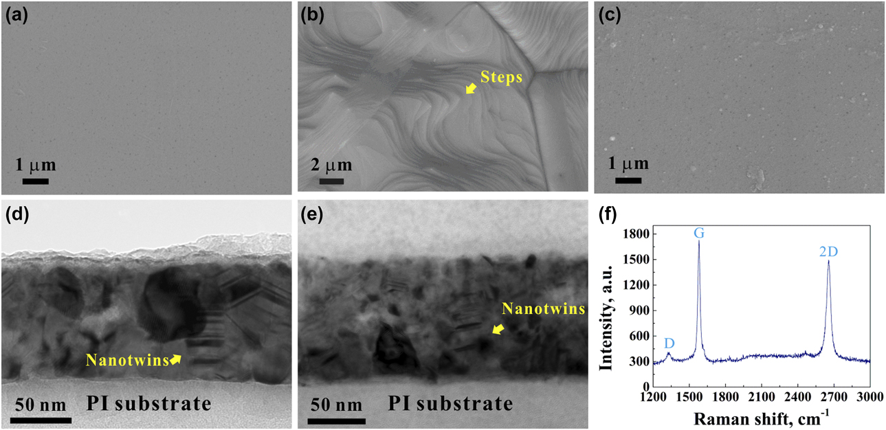
Figure 2(a) shows that the as-deposited B-Cu film is clean and even without any impurities or defects. Figure 2(b) shows a typical SEM image of the CVD graphene grown on the surface of the Cu foil. Steps and grain boundaries of the Cu foil can be clearly observed, indicating that the graphene grown on the Cu foil surface is continuous and completely covers the Cu foil [Reference Zhang, Lee, Piner, Kholmanov, Wu, Li, Ji and Ruoff52]. Morphology of the GC-Cu composite film shown in Fig. 2(c) reveals that the high-quality graphene has been successfully transferred onto the as-deposited Cu film without any macrocracks.
SEM morphologies of (a) B-Cu films deposited by PVD, the surface is clean and even without any impurities or defects. (b) Graphene on Cu by CVD, Cu surface steps and grain boundaries can be clearly observed. (c) GC-Cu films obtained by transfer graphene onto B-Cu films, high-quality graphene has been successfully transferred onto the B-Cu films without any cracks. Cross-sectional TEM view of (d) B-Cu films, (e) GC-Cu films, and (f) Raman spectrum of the GC-Cu films.
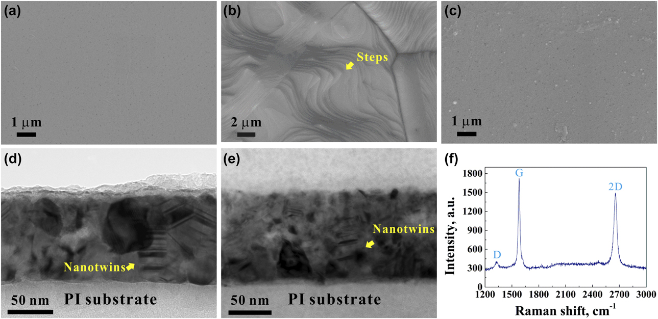
TEM cross-sectional observations of the B-Cu film [Fig. 2(d)] and the GC-Cu composite film [Fig. 2(e)] show that the thicknesses of both the B-Cu and the GC-Cu films are the same ∼100 nm. The grain size of the Cu film is in a range of 20–50 nm, and some nanotwins appeared in the as-deposited Cu film. Since the graphene grown on the Cu foil is a self-limited process and the graphene coverage is nearly 100% monolayer [Reference Li, Colombo and Ruoff53], the graphene grown on both sides of the copper foil substrate was transferred onto the Cu film to remedy the damage of monolayer graphene and ensure the Cu film fully covered by graphene, as schematically illustrated in Fig. 1. Thus, bilayer graphene was transferred onto the as-deposited Cu films. The Raman spectra of the GC-Cu films confirm the typical graphene feature characterized by the D band position of 1329 cm−1, G band position of 1581 cm−1, and 2D band position of 2656 cm−1 [see Fig. 2(f)]. The intensity ratio of the G peak to the 2D peak (I G/I 2D) is ∼1.67, and the full width at half-maximum of the 2D peak is ∼51 cm−1, indicating that the graphene film is bilayer [Reference Ferrari, Meyer, Scardaci, Casiraghi, Lazzeri, Mauri, Piscanec, Jiang, Novoselov, Roth and Geim54, Reference Ni, Wang, Kasim, Fan, Yu, Wu, Feng and Shen55].
Tensile properties
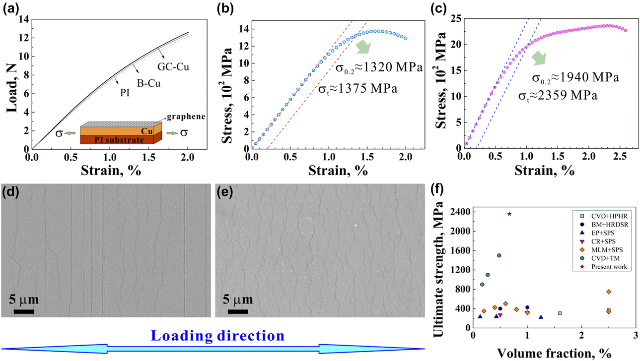
Figure 3(a) presents the load–strain curves of PI substrates, the B-Cu films, and GC-Cu composite films. The tensile stress (σ) of the B-Cu and the GC-Cu films on the PI substrate was calculated by
 $$\sigma = {1 \over {hw}}\left( {{F_{{\rm{total}}}} - {F_{{\rm{PI}}}}} \right)\quad ,$$
where F total is the force acting on the entire specimen including the PI substrate and the surface coating, F PI is the force on the PI substrate, w and h represent the gauge width and thickness of the specimens, respectively. The stress–strain curves of the B-Cu and the GC-Cu are thereby obtained based on Eq. (1) and shown in Figs. 3(b) and 3(c), respectively. The yield stress (σ0.2) of the GC-Cu film (∼1940 MPa) was enhanced by ∼47% compared with that of the B-Cu film (∼1320 MPa), due to the bilayer graphene covering. Ultimate tensile strengths (σt) of the B-Cu and GC-Cu films are ∼1375 MPa and ∼2359 MPa, respectively. It is generally accepted that the graphene reinforces metal matrix through four typical strengthening mechanisms, load transfer strengthening, grain refinement, thermal mismatch strengthening, and Orowan strengthening [Reference Chu, Wang, Li, Wang, Huang and Geng56]. For GC-Cu film presented in this work, load transfer is the most important strengthening mechanism benefited from the graphene/Cu interface [Reference Nieto, Bisht, Lahiri, Zhang and Agarwal57, Reference Xiong, Cao, Guo, Tan, Fan, Li and Zhang58]. The graphene effectively blocks the dislocations from penetrating through the graphene/Cu interface, and loads can be transferred to the graphene layer during the tensile process [Reference Kim, Lee, Yeom, Shin, Kim, Cui, Kysar, Hone, Jung, Jeon and Han38, Reference Li, Che, Liu, Liang and Xie59]. The dislocation sliding was prevented and dislocations piled up at the interface under tensile loading [Reference Kim, Lee, Yeom, Shin, Kim, Cui, Kysar, Hone, Jung, Jeon and Han38, Reference Xiong, Cao, Guo, Tan, Fan, Li and Zhang58, Reference Zhu, Zhao, Ma, Zhang, Ren, Peng, Hu, Rintoul, Bell and Yan60]. What’s more, the shear modulus and the lattice parameters mismatches between Cu and graphene may reduce the possibility of dislocations in copper slipping out of the surface, leading to the enhancement of strength for GC-Cu film [Reference Zhu, Zhao, Ma, Zhang, Ren, Peng, Hu, Rintoul, Bell and Yan60, Reference Zhao, Peng, Fu, Zhu, Hu and Yan61].
(a) Load–strain curves of PI substrate, B-Cu film and GC-Cu film; stress–strain curves of (b) a B-Cu film and (c) a GC-Cu film; SEM images of tensile cracks of (d) a B-Cu film and (e) a GC-Cu film under ∼11% applied strain; (f) a comparison of the ultimate tensile strengths of our GC-Cu films with those of the others reports, graphene-reinforced Cu matrix composites as a function of reinforcement amount of graphene, including CVD + HPHR [Reference Cao, Xiong, Tan, Ji, Amin-Ahmadi, Guo, Fan, Guo, Li and Zhang41], BM + HRDSR [Reference Kim, Lee and Han47], EP + SPS [Reference Jiang, Zhou and Liu44], CR + SPS [Reference Tang, Yang, Wang and Li46], MLM + SPS [Reference Hwang, Yoon, Jin, Lee, Kim, Hong and Jeon42, Reference Yang, Wang, Shi, Wang, Cui, Wei, Xu, Zhu and Fei43, Reference Chen, Ying, Wang, Du, Liu and Huang45], and CVD + transfer method (TM, strength measured by nanopillar compression testing) [Reference Kim, Lee, Yeom, Shin, Kim, Cui, Kysar, Hone, Jung, Jeon and Han38].
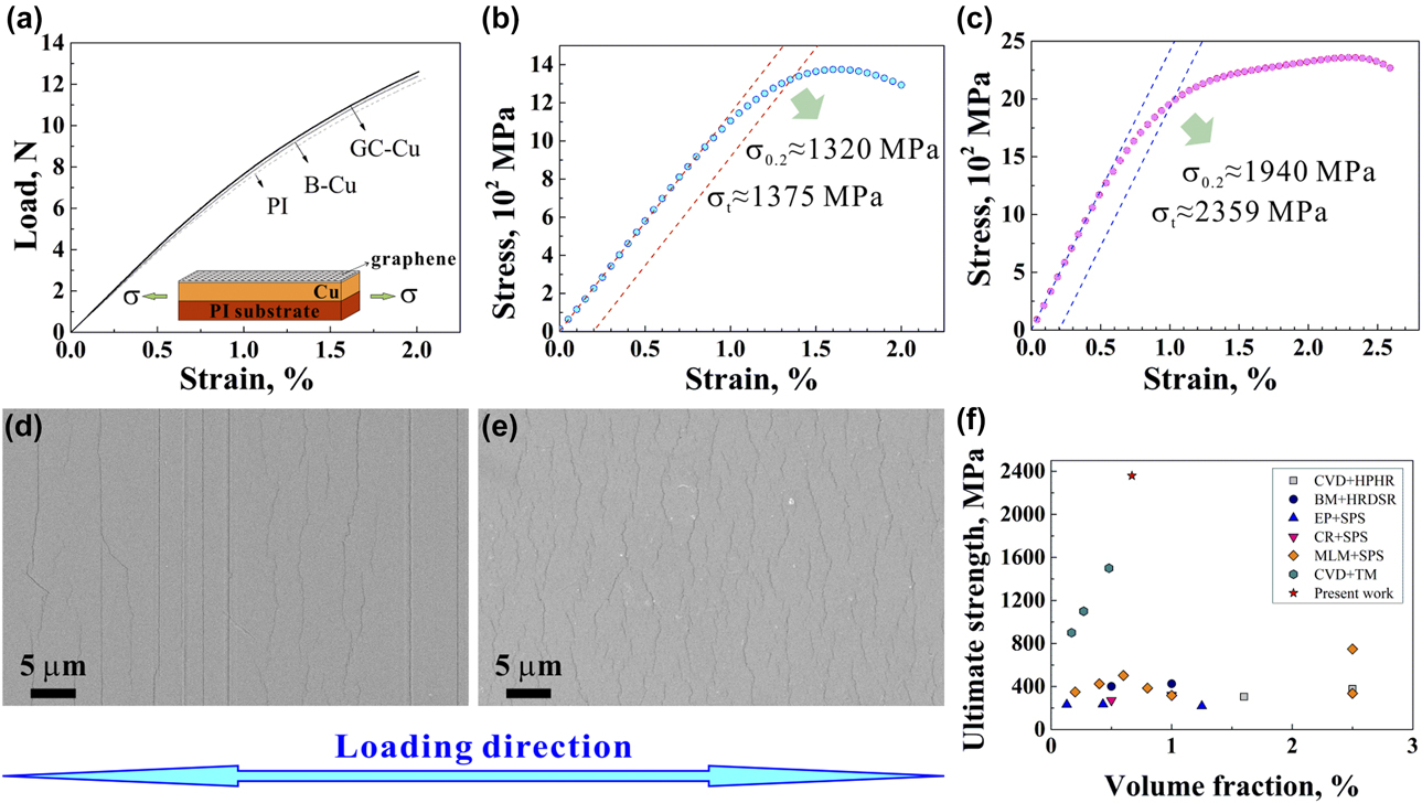
Such a strengthening effect of the GC-Cu films was also verified by SEM observation of crack morphologies shown in Figs. 3(d) and 3(e) comparatively. Since the transmittance of graphene is 97.7% [Reference Nair, Blake, Grigorenko, Novoselov, Booth, Stauber, Peres and Geim62], crack morphologies of Cu films can be identified clearly from the SEM image even though the surface is coated by bilayer graphene. Figure 3(d) shows that long and straight cracks on the B-Cu films appeared on the specimen surface, while Fig. 3(e) indicates that zigzag cracks appeared on the GC-Cu films, which are much shorter than the straight ones in the B-Cu films, implying that cracking resistance was enhanced owing to the graphene covering on the Cu film surface. Figure 3(f) presents a comparison of σt between the present GC-Cu film and the graphene-reinforced Cu matrix composites fabricated by other methods [Reference Kim, Lee, Yeom, Shin, Kim, Cui, Kysar, Hone, Jung, Jeon and Han38, Reference Cao, Xiong, Tan, Ji, Amin-Ahmadi, Guo, Fan, Guo, Li and Zhang41, Reference Hwang, Yoon, Jin, Lee, Kim, Hong and Jeon42, Reference Yang, Wang, Shi, Wang, Cui, Wei, Xu, Zhu and Fei43, Reference Jiang, Zhou and Liu44, Reference Chen, Ying, Wang, Du, Liu and Huang45, Reference Tang, Yang, Wang and Li46, Reference Kim, Lee and Han47]. It is found that the strengthening extent of the present GC-Cu composite film is evidently higher than those of the other traditional rGO-reinforced Cu matrix composites [Reference Cao, Xiong, Tan, Ji, Amin-Ahmadi, Guo, Fan, Guo, Li and Zhang41, Reference Hwang, Yoon, Jin, Lee, Kim, Hong and Jeon42, Reference Yang, Wang, Shi, Wang, Cui, Wei, Xu, Zhu and Fei43, Reference Jiang, Zhou and Liu44, Reference Chen, Ying, Wang, Du, Liu and Huang45, Reference Tang, Yang, Wang and Li46, Reference Kim, Lee and Han47] and also superior to that of nanolayered composite consisting of alternating layers of Cu and monolayer graphene [Reference Kim, Lee, Yeom, Shin, Kim, Cui, Kysar, Hone, Jung, Jeon and Han38]. Thus, the present Cu films covered by high-quality bilayer graphene possess the highest ultimate tensile strength, which would be of great potential for high-performance stretchable devices.
Bending properties
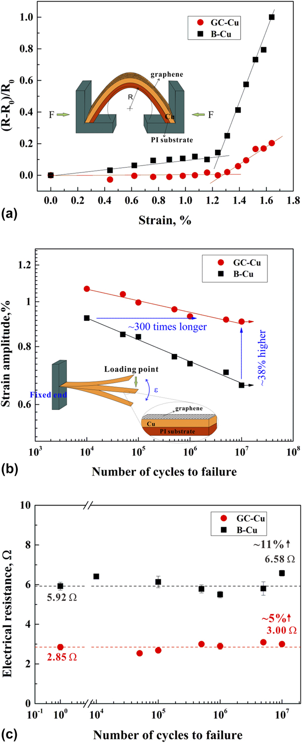
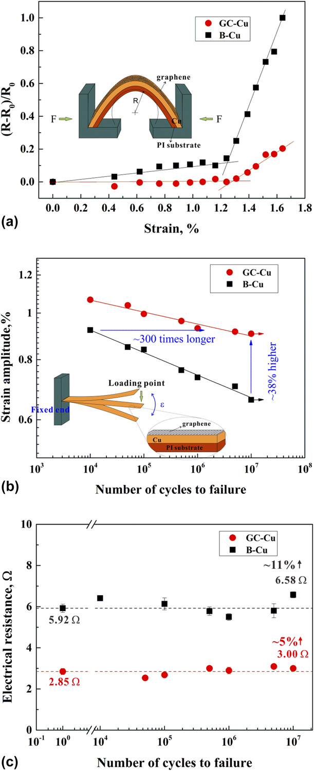
To examine the electrical properties of the GC-Cu composite electrodes subjected to mechanical bending, the simply supported beam bending test was conducted on home-made apparatus [Reference Ni, Zhu, Pei, Gong, Sun and Zhang63, Reference Zhu, Zhang, Gao and Zhang64] with simultaneously measuring the real-time electrical resistance (R) of the films as the applied bending strain (ε) increased from 0 to 1.64%. A relative resistance change  $\left( {\tilde{R} = {{R - {R_0}} \over {{R_0}}}} \right)$ of the B-Cu films and GC-Cu films as a function of ε are shown in Fig. 4(a), which can be divided into two stages. In the first stage,
 $\tilde{R}$ of the B-Cu films slightly increases, while that of the GC-Cu films basically remains invariable. The main reason is that the GC-Cu film has a higher elastic modulus and yield strength, resulting in a delay of yielding compared with the B-Cu films with lower elastic modulus and yield strength. In the second stage, both the B-Cu and GC-Cu specimens have an evident increase in
 $\tilde{R}$ due to the formation of damage. However, the increase rate of the GC-Cu film is lower than that of the B-Cu film, indicating that the coated graphene of the GC-Cu films can effectively resist the evolution of damage with the increase in bending strain [Reference Zhang, Lu, Pei, Li, Wang and Tieu65]. Unexpectedly, the fitted lines of these two stages for B-Cu films and GC-Cu films almost intercepted at the same strain (∼1.3%), which may be due to the weak interface bonding between graphene and Cu [Reference Nieto, Bisht, Lahiri, Zhang and Agarwal57, Reference Wang, Zhang, Zhao and He66]. It is believed that the damage formation of the films would be further delayed if the adhesion of the graphene/Cu interface had been improved through optimizing graphene transfer method.
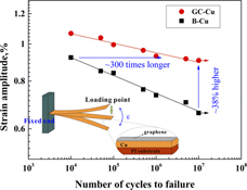
(a) Normalized resistance change curves versus applied strain of B-Cu films and GC-Cu films under bending tests; (b) S–N curves of the applied strain amplitudes versus numbers of cycles to failure of B-Cu films and GC-Cu films under cyclic bending loads; (c) Electrical resistance of the B-Cu and GC-Cu films before and after cyclic bending tests.
Bending fatigue properties
Typical relationship between the applied strain amplitude (Δε/2) and the fatigue life (N f) for B-Cu and GC-Cu films is presented in Fig. 4(b). It is clear that the fatigue life of the GC-Cu films was enhanced by ∼300 times compared to the B-Cu films. Especially the critical fatigue strain amplitudes corresponding to the lowest strain amplitudes for fatigue cracking (0.91% for GC-Cu films) is ∼38% higher than that of the B-Cu ones (0.66%). Moreover, besides great improvement in the fatigue strength, a simultaneous enhancement of conductivity during bending fatigue is shown in Fig. 4(c). Initial resistances of the as-prepared B-Cu and the GC-Cu films are 5.92 Ω and 2.85 Ω, respectively, as indicated by dash lines in Fig. 4(c). After 107-cycle bending tests, the resistance of the B-Cu films increased by ∼11% (6.58 Ω), while that of the GC-Cu films only increased by ∼5% (3.00 Ω). Furthermore, the less increase in the GC-Cu film resistance indicates that fatigue cracks would not form in the films and the electrical performance of the films would not be weakened if the GC-Cu films were subjected to the strain amplitude less than 0.91% and even for over 107 cycles.
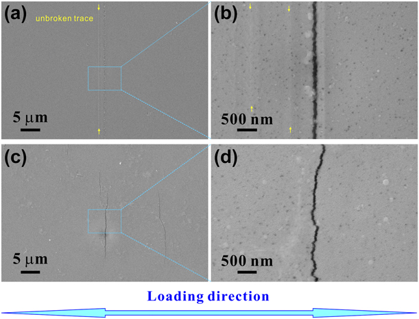
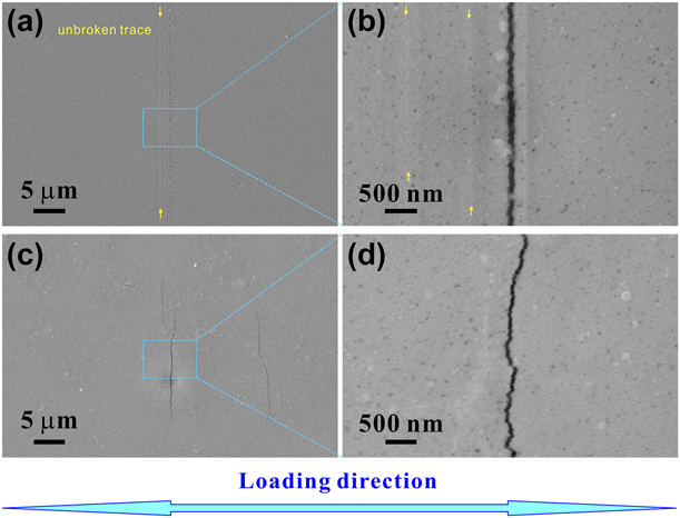
Figure 5(a)–5(d) present SEM images of fatigue cracking behavior of the B-Cu films and GC-Cu ones after repeatedly bending at Δε/2 = 0.96% for 106 cycles, respectively. Some parallel, long, straight fatigue cracks and some unbroken traces before the crack initiation in the same direction were observed on the B-Cu film [see Figs. 5(a) and 5(b)], while for the GC-Cu film, the formation of shorter and fewer zigzag cracks [see Figs. 5(c) and 5(d)] indicates that the crack propagation was prevented by the transferred graphene on the surface of the GC-Cu film. The fact that cracks in the GC-Cu films became more tortuous than that in the B-Cu ones at Δε/2 = 0.96% demonstrates that the crack propagation resistance is effectively enhanced by graphene coated on Cu films.
SEM images of bending fatigue cracks of (a) and (b) B-Cu films, and (c) and (d) GC-Cu films after 106 cycle loading, the strain amplitude is 0.96%.
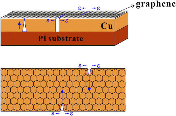
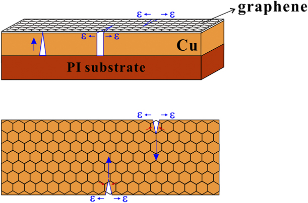
It is well accepted that the fatigue life is composed of crack initiation life and crack propagation life. In the fatigue crack initiation stage, the coated graphene of GC-Cu films with higher yield strength acted as a barrier impeding the formation of extrusions of the Cu film, which can effectively resist the crack initiation. In the fatigue crack propagation stage, once cracks began to propagate in the Cu film of the GC-Cu films, the as-coated graphene still subjected to elastic deformation due to the ultrahigh elastic modulus, which would produce an opposite force to resist the crack opening in the Cu layer, as shown in Fig. 6. This means that the locally high stress at the crack tip was somewhat screened by the graphene layer and a part of the energy driving crack propagation was absorbed by the coated graphene on the Cu films. Thus, the crack propagation distance of the GC-Cu films became shorter than that of the B-Cu ones when the same strain amplitude was applied. Fatigue cracks initiated from the Cu layer then stopped by the graphene interface has also been confirmed by Hwang et al. with cross-sectional SEM and TEM observations [Reference Hwang, Kim, Kim, Lee, Lim, Kim, Oh, Ryu and Han12]. And also, the graphene/Cu interface with strong sp 2 bonding can act as an effective barrier for deflecting the fatigue cracks under cyclic bending [Reference Hwang, Kim, Kim, Lee, Lim, Kim, Oh, Ryu and Han12, Reference Kim, Lee, Yeom, Shin, Kim, Cui, Kysar, Hone, Jung, Jeon and Han38]. This is the reason for the GC-Cu films with longer fatigue life and higher fatigue limit than that of the B-Cu ones. The present finding not only provides a potential candidate for high-performance electrodes of the flexible devices but also reveals a new idea to design strong composites by employing graphene to suppress the formation and development of mechanical damage.
Schematic illustration of cracks propagation in GC-Cu films under cyclic bending tests.
Conclusion
Enhanced by surface-covered bilayer graphene, the yield strength of the GC-Cu composite film is evidently enhanced by 47%, from ∼1320 MPa for the B-Cu films to ∼1940 MPa, and the ultimate tensile strength of the GC-Cu films is improved by 72% (from ∼1375 to ∼2359 MPa). The critical strain for fatigue crack initiation of the B-Cu and GC-Cu films was determined as ∼1.3%. The critical fatigue strain amplitude corresponding to the lowest strain amplitude for bending fatigue cracking of the GC-Cu films is improved from 0.66 to 0.91%, while the electric resistance of the GC-Cu films only increased by ∼5% after 107-cycle bending fatigue. It demonstrates that the bilayer graphene-covered Cu films on a PI substrate have a good combination of high electrical performance and excellent durability against mechanical deformation.
Experimental
Fabrication of B-Cu films
Cu films (target purity: 99.99%) with thickness of ∼100 nm were deposited onto a PI (Dupont®, Wilmington, Delaware, USA) substrate with dimensions of 40 mm × 40 mm × 125 μm by radio frequency magnetron sputtering (JGP 560 high-vacuum magnetron sputtering system) under ultra-high vacuum (<10−3 Pa) with the working pressure of 0.5 Pa, the deposition rate was ∼0.185 nm/s, and the flow rate of argon was 25 sccm. Prior to the deposition, the substrates were ultrasonically cleaned in ethanol and deionized water to remove the contamination.
Fabrication of GC-Cu composite films
High-quality graphene was grown on both sides of a copper foil (99.8%, Alfa-Aesar, Shanghai, China, Item No. 13382) and then transferred onto the B-Cu film to make sure the Cu film is fully covered by graphene. The upper side surface of the graphene on the copper foil was spin-coated (4000 rpm × 40 s) with a layer of poly-methyl methacrylate (PMMA) (MW 350,000; 46 mg/mL in chlorobenzene) [Reference Zhang, Lee, Piner, Kholmanov, Wu, Li, Ji and Ruoff52, Reference Chen, Wu, Mishra, Kang, Zhang, Cho, Cai, Balandin and Ruoff67]. Edges of the specimen were cut by a sharp knife to make sure the copper foil in the middle layer exposed outside. The copper foil was etched away by dipping in an aqueous ammonium persulfate solution (0.1 M) after the PMMA cured. The PMMA-coated graphene was floated on the solution and rinsed several times by deionized water after the copper foil was completely dissolved. The PMMA/graphene was transferred onto the Cu film, and the specimen was dried in air for 30 min and then in vacuum drying chamber for 30 min to evaporate out the excess water between graphene and Cu. Subsequently, the PMMA coating was removed using acetone and the GC-Cu composite film was obtained.
Microstructure characterization
Surface morphologies of the B-Cu film, the GC-Cu film, and fatigue cracks of the samples after tensile or fatigue tests were observed by a field-emission scanning electron microscope (FE-SEM; Zeiss, Supra 35, Oberkochen, Germany). Cross-sectional view of the films was measured by a field-emission transmission electron microscope (FE-TEM; FEI, Tecnai 20, Hillsboro, Oregon). To evaluate the quality of transferred graphene, a Raman spectroscopy was measured with a XPLORA full-automatic Raman spectrometer with a laser wavelength of 638 nm and a 50× objective lens. Electrical resistance of the film was measured by a digital multimeter (Agilent 34410A, Keysight, Shenzhen, China) with a resolution of 10−3 Ω.
Tensile test
The tensile samples were cut into 16 mm in length and 2 mm in width, and the gauge length and the gauge width of the tensile specimen are 10 mm and 2 mm, respectively. Tensile tests were performed using a microforce testing system (MMT-101NV-10 SHIMADZU, Kyoto, Japan) with samples mounted on a template made of card-stock.
Monotonic bending test
The simply supported beam bending samples with a length of 16 mm and a width of 2 mm were prepared and then mounted on card-stocks. Monotonic bending tests were performed with measuring the real-time electrical resistance of the film simultaneously. The applied strain (ε) was calculated according to our previous report [Reference Yang, Zhang, Tan, Luo and Zhang68].
Repeatedly bending fatigue test
Cantilever beam-type specimens with a gauge length of 6 mm and gauge width of 2 mm were installed on a home-made system [Reference Dai, Zhu and Zhang69]. A constant deflection with 50 Hz loading frequency was applied to the free end of the specimens, inducing a bending curvature (κ) of ± 0.173. The strain (ε) applied to the samples can be calculated following the method reported previously [Reference Yang, Zhang, Wan and Zhang70].
Acknowledgments
This work was supported by the National Natural Science Foundation of China (NSFC, Grant Nos. 51671050, 51971060, and 51571199).