Introduction
In the modern nanoscience, diamondoids, novel carbon-based functional nanostructures, have recently received tremendous interests. Diamondoids (or diamond molecules) are nanometer-sized, hydrogen-terminated diamond–like, saturated hydrocarbons [Reference Roth, Leuenberger, Osterwalder, Dahl, Carlson, Tkachenko, Fokin, Schreiner and Hengsberger1], which process great potential in nanotechnology like its cousins graphene, carbon dots, and nanodiamond [Reference He, Huang and Li2, Reference Zhang, Ziemer, Zhang, Ramirez, Li, Wang, Hope-Weeks and Weeks3, Reference Zhang, Hikal, Zhang, Bhattacharia, Li, Panditrao, Wang and Weeks4, Reference Zhang, Ji, Su, Weeks, Zhang and Deng5], such as drug delivery, DNA delivery, nanorobotics, and nanolubrication [Reference Zhang6], since diamondoids are biocompatible and ultrahard. Adamantane, amine-derivatives of the lower diamondoid, has been employed in pharmaceutical applications as antiviral and anti-Parkinson’s agents [Reference Schnell and Chou7]. Diamondoids consisting of different numbers of diamond–crystal cages own a large variety of size and can easily be chemically modified [Reference Fyta8], which can be used to tune the optical and electronic properties [Reference Richter, Wolter, Zimmermann, Landt, Knecht, Heidrich, Merli, Dopfer, Reiss, Ehresmann, Petersen, Dahl, Carlson, Bostedt, Moller, Mitric and Rander9]. For example, diamondoids can be chemically connected onto metallic surface by thiol groups to form a self-assembled layer, which process a negative electron affinity (NEA) and a strong monochromatic emission [Reference Roth, Leuenberger, Osterwalder, Dahl, Carlson, Tkachenko, Fokin, Schreiner and Hengsberger1]. Theoretically, a larger interlinked nanostructure can be fabricated from the lower diamondoids and their derivatives [Reference Xue and Mansoori10]. Adamantane, a cycloalkane with formula C10H16, is the smallest diamondoid, which the carbon atoms of adamantane are sp 3 bonded to form a cage in the diamond lattice [Reference Fort and Schleyer11]. Diamantane C14H20 and triamantane C18H24 are generated by fusing two and three adamantine cages together, respectively. These structures are called lower molecules and their sizes are smaller than 1 nm. The rest of entire diamondoid series consists of increasing number of cages, which processes multiple isomers for a given number of cages [Reference Zhou, Brittain, Kong, Xiao, Meng and Sun12]. In 2002, Dahl et al. reported that higher diamondoids containing four to eleven cages ranged in the size of 1–2 nm [Reference Dahl, Liu and Carlson13], which were isolated from petroleum and then purified by pyrolysis and chromatography.
Traditional one-dimensional (1D) fiber material is in micro scale, which is employed in wide range [Reference Lu, Wang, Yao, Gou, Hui, Xu and Fu14]. Now tremendous attempts have been devoted to achieve 1D nanomaterials, such as carbon nanotubes, carbon nanofibers, and diamond nanowires [Reference Choi, Rhee and Park15]. Because of superior properties, 1D organic nanostructures have attracted lots of interests [Reference Yamamoto, Fukushima, Suna, Ishii, Saeki, Seki, Tagawa, Taniguchi, Kawai and Aida16]. Especially, by combing the variety of 1D nanostructure, the 1D nanomaterials own large numbers of promising electronic, optical, and optoelectronic applications in photovoltaics, nanophotonics, nanoelectronics, and sensing [Reference Jiang, Dong, Meng, Li, He, Wei, He and Hu17]. Diamond nanowires process theoretically higher aspect ratio than zero dimensional (0D) diamond nanoparticles [Reference Li, Zhang, Qiu, Wang, Van and Zhang18], which are attracting a large number of interests. The traditional way to obtain diamond nanowires is top–down etching, briefly, bulk diamond crystal film was masked, and continually etched by plasma to produce vertically aligned diamond nanowires [Reference Janssen and Gheeraert19]. Chemical vapor deposition (CVD) is the second type to produce one-dimensional (1D) diamond nanowires [Reference Hsu, Cloutier, Palefsky and Xu20]. However, both two methods need complicated and expensive facilities and processes compared to other 1D material, like carbon nanotubes [Reference Zhao, Ren, Ling, Lukatskaya, Zhang, Van Aken, Barsoum and Gogotsi21], nanofibers [Reference Mao, Simeon, Rutledge and Hatton22], and metal nanowires [Reference Chandni, Kundu, Kundu, Ravishankar and Ghosh23].
Particle aggregation refers to formation in a suspension by destabilization of colloidal systems, which is widely applied and studied [Reference Zhang, He, Sushko, Liu, Luo, De Yoreo, Mao, Wang and Rosso24, Reference Zhang, Shen, Liu, Kerisit, Bowden, Sushko, De Yoreo and Rosso25]. During this destabilization process, particles that are well dispersed in the liquid phase contact to each other to spontaneously form aggregates. By this method, particle aggregation has been formed, it is not easily broken, which means it is normally an irreversible process. Usually, particle aggregates to the bottom of the container as sedimentation, which limits its application in specific nanostructure fabrication.
Diamondoids, like diamond, are NEA material [Reference Roth, Leuenberger, Osterwalder, Dahl, Carlson, Tkachenko, Fokin, Schreiner and Hengsberger1], which can be used to prepare nanostructure through cathodic electrophoretic deposition (EPD) [Reference Singh, Nayak, Nanda, Jena, Bhattacharjee and Besra26]. Previous studies presented that the diamond nanostructures were successfully produced by cathodic EPD [Reference Li, Zhang, Qiu, Wang, Van and Zhang18]. However, to the best of our knowledge, no solution method has been applied to fabricate vertical diamondoid nanowires and orderly diamondoid nanocluster array. Electrophoresis with template is one of the most efficient and simple methods for synthesizing hierarchical branched nanostructures [Reference Limmer, Seraji, Wu, Chou, Nguyen and Cao27]. In addition, complicated 1D nanostructures, like branched nanostructures have attracted numerous of interests due to great function [Reference Ye, Regulacio, Zhang, Loh and Han28]. Various techniques have been developed to achieve different type hierarchical branched nanostructures; however, the complicated manufacturing processes severely limit their application [Reference Hasan, Schroers and Kumar29]. Therefore, exploring a simple method to achieve hierarchical branched nanostructures is a great challenge.
In the current study, triamantane was used to achieve diamondoid nanowires through porous anodic aluminum oxide (AAO) film (as shown in Fig. S1). By introducing electric field, the diamondoid molecules were forced into the AAO cylindrical holes to form one-dimensional (1D) nanowires. A critical point drying process is necessary to obtain vertical diamondoid nanowires. The diamondoid nanowire bundles were fabricated without critical point drying process. To well improve the mechanical properties of diamondoid nanowire, two different heating processes were employed. After a two-step thermal treatment, the orderly diamondoid nanoclusters consisting of hierarchical branched nanowires were achieved, whereas a one-step thermal method failed with collapsed diamondoid nanowires. In addition, the mechanism of diamondoid nanowire/nanotube formation and simple explanation of hierarchical branched diamondoid nanowires formation were introduced. This approach opens a new pathway to assemble diamondoid nanowires array and branched nanowire cluster, which can be employed for applications in chemical sensors, light energy conversion devices, and nanoscale electronic and optoelectronic devices [Reference Narasimha, Ge, Fabbri, Clay, Tkachenko, Fokin, Schreiner, Dahl, Carlson, Shen and Melosh30, Reference Yan, Hohman, Li, Jia, Solis-Ibarra, Wu, Dahl, Carlson, Tkachenko, Fokin, Schreiner, Vailionis, Kim, Devereaux, Shen and Melosh31, Reference Sarap, Partovi-Azar and Fyta32, Reference Sarap, Partovi-Azar and Fyta33]. The synthesized nanostructures with high aspect ratio can be used in dynamic tuning of surface wetting, drug delivery, immunoassay chips, MEMS actuators, field emission, and superhydrophobic surface [Reference Zhang, Lo, Taylor and Yang34].
Results and discussion
In this article, the triamantane was achieved from the higher diamondoids which is developed by Dr. Jeremy Dahl. The obtained triamantane was first characterized by a TA Q20 (TA Instruments Inc., New Castle, DE) to perform differential scanning calorimetry (DSC). As shown in Fig. S2, two peaks were observed in the DSC curve. One peak at 156 °C was resulted from the solid–solid transition of the diamond crystals. The peak at 225 °C was derived from the melting transition of the diamond crystals, which is similar to the previous literature [Reference Mansoori35].
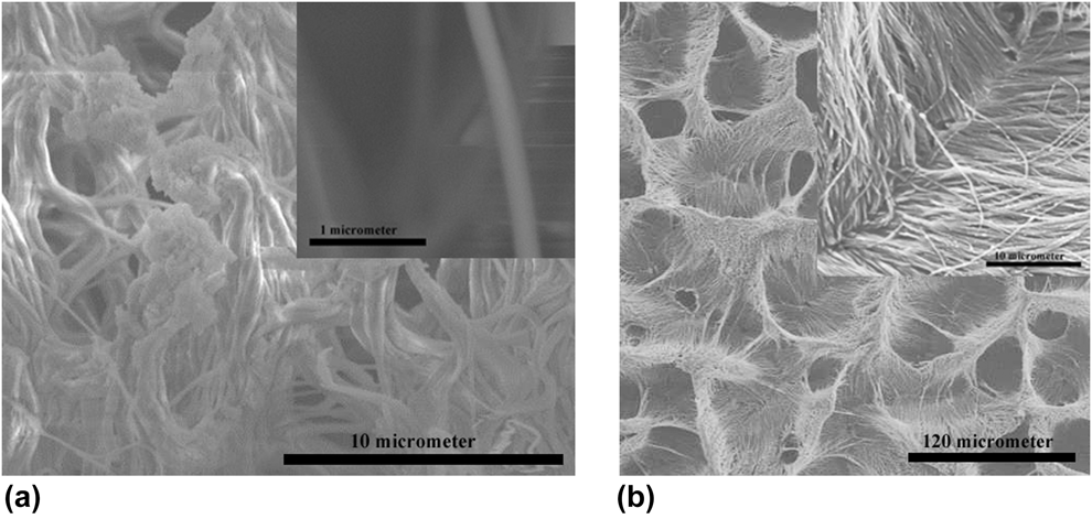
To achieve diamondoids nanowire array, triamantane was used as raw material in this study. The triamantane discovered by Dr. Jeremy Dahl was first well dispersed in toluene by bath sonication for 15 min. Then the electrophoresis process was employed when an AAO film–attached silicon substrate was connected as a working electrode (as shown in Fig. S1). At the electrophoresis parameter of 30 V, 1 mA and one-hour continuous deposition, solid diamondoid nanowires were produced. After fabrication, the AAO template was etched by 1 M sodium hydroxide solution and dried via a heating plate; the surface morphology and structure of as-prepared diamondoid nanowires were characterized by scanning electron microscopy (SEM) via Hitachi S-4300 (Hitachi Appliances Inc., Tokyo, Japan), and SEM images are depicted in Fig. 1. Without critical point drying and thermal heating, diamondoid nanowires with unique diameter randomly laid on the silicon substrate, leading to failure of achieving vertically standing diamond nanowire array, because of the residual stress during dry process. As shown in Fig. 1(a), the curving diamondoid nanowires wrap each other to form nanowire bundles, which presented random diamondoid nanostructures that limit its further application in electronic devices. In addition, a knot without specific geometry was clearly observed on the top of each bundle, which might be the residual alumina that has not been removed by sodium hydroxide. An individual diamondoid nanowire is presented in the inset figure of Fig. 1(a). The diameter of diamondoid nanowires was exactly 200 nm, which is reasonable that the size of diamondoid nanowire is determined by the pore size on the AAO template. The surface of diamondoid nanowires was very smooth, which demonstrates that the particle aggregation of triamantane is successful and the size of triamantane is very small.
SEM images of (a) random twisted diamondoid nanowires, and the inset is individual diamondoid nanowire without critical point drying and heating treatment; (b) SEM images and magnified SEM images (the inset) of diamondoid nanowires with critical point drying and one-step heating treatment.

To achieve vertically aligned diamondoid nanowire array, critical point drying was employed to remove solvent to ensure that nanowires would not fall. After fabrication, the AAO template was etched by 1 M sodium hydroxide solution, and then critical point drying was employed to achieve vertically aligned diamondoid nanowires. Briefly, a series of mixture of water/ethanol (90/10, 70/30, 50/50, 30/70, 20/80, 10/90, and 0/100) with small ethanol concentration gradient were used in the solvent exchange process. Finally, the aqueous solution was exchanged by 100% ethanol and the 100% ethanol was removed by critical point drying instrument. As shown in Fig. S3, although the diamondoid nanowires were clearly separated, and not twisted to form nanobundles, the nanowires were not perfectly vertically aligned and the displacement between two nanowires nearly existed, which indicated the modulus of the diamondoid nanowires was low and the potential to form branched nanostructures after heat treatment. The diameter of diamondoid nanowires was also around 200 nm, which is derived from the pore size of the AAO template.
To well improve the mechanical property of the nanowires and to form specific diamondoid branched nanostructure array, two different heating treatments were performed. In one-step method, the nanowires were heated by a single-stage heating process at 226.5 °C for 1 h, which is 5 °C higher than the melting point of triamantane based on the DSC thermograms of the triamantane [Reference Mansoori35]. The morphology of nanostructure was characterized via SEM. As shown in Fig. 1(b), the diamondoid nanowires combined each other and collapsed without specific structure. In addition, after heating treatment, residual stress was left on the nanowires. As shown in the inset figure of Fig. 1(b), in each individual nanowire, lots of bubbles exist and they are not homogeneously distributed, which demonstrated that this approach had failed.
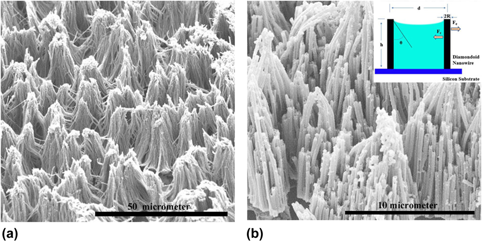
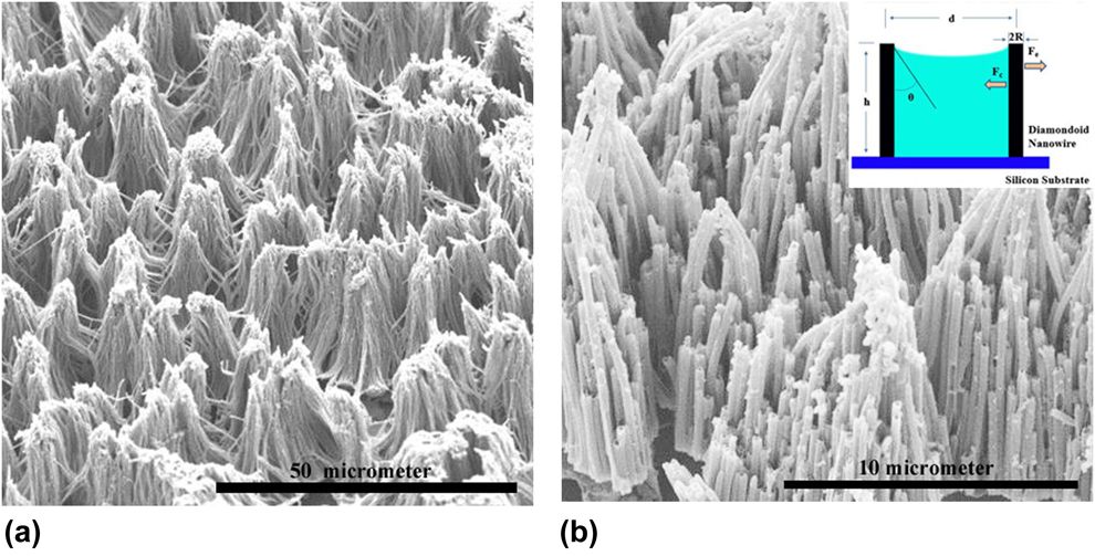
To form specific diamondoid nanostructure array, a two-step thermal treatment was performed to achieve orderly diamondoid branched nanostructures array and to remove the residual stress. As shown in Fig. 2(a), orderly nanocluster arrays were obtained on the silicon substrate, although the nanoclusters were not perfectly in the same size and the distances between nanoclusters were not uniform. The vertical nanoclusters consisting several triamantane nanowires are shown in a large size, which were much better than the collapsed nanowires and could be used in electronic field. It also presented that aligned nanowires could be achieved when the synthesis height is around 10 µm. To understand more detailed morphology information about the triamantane nanoclusters, a single nanocluster was amplified. As shown in Fig. 2(b), it was observed that the length of triamantane nanowires in the nanocluster was not the same, several nanowires around the core of nanocluster was much shorter than that in the core. The reason might be that the high heating temperature induced that some nanowires and some parts of nanowire were damaged. In addition, the bottom of diamondoid nanowires connected each other, which indicates that the nanowire cluster array was achieved with a hierarchical and branched structure. Fig. 2(b) also showed the top of nanoclusters with residual alumina oxide. Some long nanowires were still depicted in a collapsed state, which demonstrates the heating treatment could not successfully improve the modulus of triamantane nanowires. The inset figure of Fig. 2(b) presented the schematic illustration of the forces acting on the two neighboring diamondoid nanowires, where d stands for the distance between two nanowires, h for the height of nanorod, θ is the static contact angle of solvent on flat diamondoid nanowire surface, R is the radius of nanorod. Fe is the elastic resistant force to endure bending or distortion, which is proportional to the Young’s modulus of diamondoid nanowire, while inversely proportional to the cube of nanowire height. Due to the low Young’s modulus and large height (60 µm), the Fe is tiny in this diamondoid nanowire system, which cannot withstand the large capillary force F c, leading to the collapse of diamondoid nanowires into the nanocluster structure. To further develop the vertically aligned diamondoid nanowires, the modulus and length of nanowires should be carefully designed.
(a) SEM image of diamondoid nanowire cluster after two-step heating treatment; (b) amplified SEM image of diamondoid nanowire cluster, and the inset is schematic illustration of the driving force in clustering.
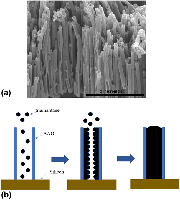
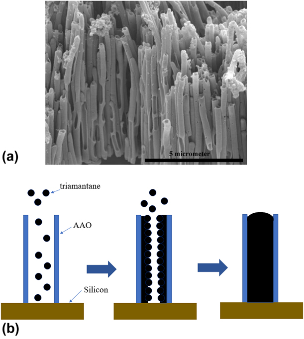
As shown in Fig. 3(a), diamondoid nanotubes were clearly found, which indicates that the diamondoid continuously diffused into the hole and deposited. According to the nanostructure of the 1D diamondoid nanowire/nanotube depicted in the SEM images, a detailed synthesis mechanism is presented in Fig. 3(b). The synthesis mechanism may not be similar to our previous work where acid-treated diamond nanoparticles containing electron-defect carboxyl and hydroxyl groups were employed to generate diamond nanowire/nanotubes [Reference Li, Zhang, Qiu, Wang, Van and Zhang18]. The diamondoids are NEA material [Reference Roth, Leuenberger, Osterwalder, Dahl, Carlson, Tkachenko, Fokin, Schreiner and Hengsberger1], which can be driven to the cathode in the direct current (DC) electrical field, whereas the AAO is a Lewis acid [Reference Cao, Xu, Hong, Liu, Yin, Li, Tie and Xu36]. Therefore, a reasonable mechanism may be as follows in this article. In the first step, the NEA nature of the diamondoid may lead them to the cathode under the DC electric field. Second, the diamondoid may be ready to be ionized in acetonitrile to generate H+, and these ionized diamondoid may be easy to attach onto the AAO surface walls by electrostatic force. At last, with increasing fabrication, the diamondoid may continuously attach onto formed diamondoid surface wall to finally build diamondoid nanowires.
(a) SEM images of diamondoid nanowires and (b) mechanism of diamondoid nanowire fabrication.
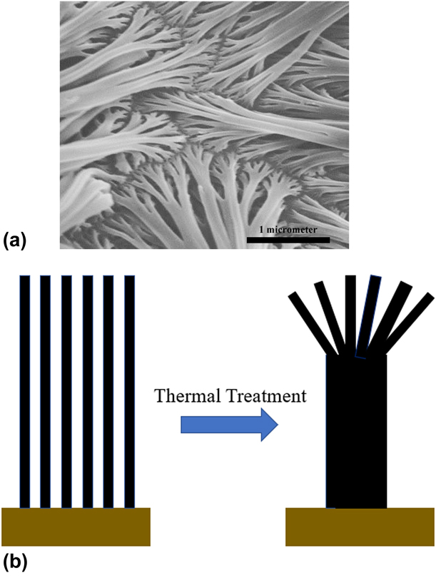
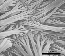
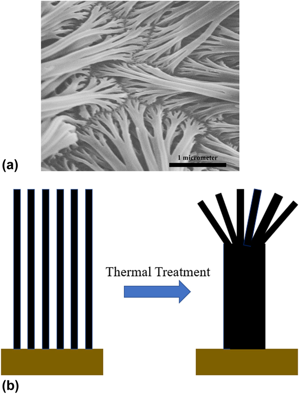
Surprisingly, clear hierarchical branched diamondoid nanowires were found in SEM image. As shown in Fig. 4(a), the diamondoid nanowires presented hierarchical branched nanostructure that was similar to the novel metal nanowires or silicon nanotubes in previous publications [Reference Hasan, Schroers and Kumar29]. Chen et al. produced branched silicon nanotubes and metal nanowires via AAO-template–assistant approach, in which the AAO template was fabricated in a complicated process. In addition, Kumar’s group achieved branched metallic glass nanowire via hierarchical patterning [Reference Hasan, Schroers and Kumar29]. The above methods to produce the branched nanowires had understanding disadvantages, complicated manufacturing, high cost, etc. However, in this method, the hierarchical branched diamondoid nanowires were fabricated via a facile two-step approach, including cathodic EPD and thermal treatment, which is much simpler compared to abovementioned manufacturing process. These hierarchical branched diamondoid nanowires were found at the interface between the nanowires array and the silicon substrate. The diameter of these hierarchical branched diamondoid nanowires at bottom was sum of diameter of branches at the top of diamondoid nanowires, which the top of these hierarchical branched diamondoid nanowires had a uniform diameter around 200 nm, which is the diameter of single diamondoid nanowire. These results demonstrate that the hierarchical branched diamondoid nanowires are combined of several diamondoid nanowires with an integrated diamondoid nanowire at bottom and a few separated diamondoid nanowires at top. As presented in Fig. 4(b), a thermal treatment around 241.5 °C, which is much higher than the melting point of triamantane, was employed to improve the mechanical properties of diamondoid nanowires array. During this heating treatment, the triamantane was melted and combined together at the bottom of diamondoid nanowires, whereas the top of diamondoid nanowires was easy to collapse due to poor mechanical properties, which make them hard to contact each other to combine them together. After thermal treatment, the diamondoid nanowires at bottom were combined to be an integrated nanowire. On the other hand, the diamondoid nanowires at top were cooled to form branched diamondoid nanowires. To well understand the formation of hierarchical branched diamondoid nanowire during thermal treatment, a systematical experiment will be performed in detail and the mechanism of hierarchical branched diamondoid nanowire will be presented in the following article.
(a) SEM images of hierarchical branched diamondoid nanowire and (b) schematic figure of hierarchical branched diamondoid nanowire formation.
Conclusion
In this article, hierarchical branched diamondoid nanostructures were fabricated via a facile approach combining cathodic EPD and two-step thermal treatment. Triamantane was employed as raw material to achieve diamondoid nanowires via porous AAO film, and vertical diamondoid nanowires were achieved after critical point drying. A two-step thermal treatment was applied to achieve hierarchical branched diamondoid nanowires array, which might open a new approach to fabricate novel nanostructure array. In addition, the mechanism of diamondoid nanowire/nanotube formation and hierarchical branched diamondoid nanowires formation were introduced.
Methodology
In the present study, triamantane, three-cage diamondoids, were used to produce diamondoid nanostructures. It was obtained from the higher diamondoids discovered by Dr. Jeremy Dahl. Anhydrous toluene (99.8%) was purchased from Sigma Aldrich (Burlington, MA). Commercial AAO film was ordered from Whatman Ltd (Pittsburgh, PA). The size of AAO pore is around 200 nm and the thickness of AAO film is around 60 µm. Series 2400 SourceMeter from Keithley Instrument, Inc. (Beaverton, OR), was used to control the electrophoresis process.
10 mg triamantane was dissolved in 20 mL toluene by a bath sonication for 15 min. At the same time, AAO film was attached to a silicon wafer by Ag/epoxy conductive binder, which was used as a working electrode. The diced silicon substrates were first achieved by a glass knife and were cleaned by a mixture solution consisting of NH4OH (20% solution), H2O2 (30% solution), and deionized water (DI water) with a ratio at 5:1:1 and heated around 60 °C for 3 h. After that, these diced silicon substrates were rinsed with DI water and dried at 70 °C under a nitrogen atmosphere, and then were stored in desiccators before using [Reference Zhang, Ji, Su, Weeks, Zhang and Deng5]. This silicon/AAO–based working electrode was assembled onto the cathode, and a platinum wire was used on the anode as a counter electrode. Then both anode and cathode were put into the toluene solution. During the cathodic electrophoretic deposition, a Series 2400 SourceMeter from Keithley Instrument, Inc., was used as a power source, and the voltage was 30 V and current was 1 mA (as shown in Fig. S1). The distance between the cathode and anode was 1 cm.
After 1 h, the silicon wafer was transferred into 1 mol/L sodium hydroxide solution to remove the AAO template for another 1 h. However, the nanowires obtained in this way laid on the substrate randomly. To achieve vertically aligned diamondoid nanowire arrays, critical point drying method was applied. The AAO template adhered to silicon wafer was first etched by sodium hydroxide solution and then rinsed with DI water and ethanol mixture (90/10, 70/30, 50/50, 30/70, 20/80, 10/90, and 0/100) for 15 min to remove water, respectively. Finally, the vertically aligned diamondoid nanowire arrays were achieved by removing ethanol via the supercritical point drying technique. To well improve the mechanical properties of diamondoid nanowires, two various heat treatment processes were employed, including a one-step method and a two-step method. In the one-step method, the diamondoid nanowire array was heated up to 226.5 °C for 1 h. This temperature (226.5 °C) is little higher than the melting point of triamantane [Reference Mansoori35]. On the other hand, in the two-step method, the diamondoid nanowire array was first heated at 241.5 °C for 2 h and cooled down in the oven. At the second stage, the diamondoid nanowire array was heated at 141.5 °C to remove the residual stress.
Differential scanning calorimetry (DSC) was performed on a TA Q20 (TA Instruments, Inc.) with a heating rate of 2 °C/min to analysis thermodynamic properties of triamantane. In addition, all the nanowire arrays were characterized by scanning electron microscopy (SEM), which were performed on Hitachi S-570 and S-4300 (Hitachi Appliances Inc., Japan). Before operating on the Hitachi S-570 and S-4300, all the nanowire arrays were coated with Au film by a sputter coating instrument.
Supplementary material
To view supplementary material for this article, please visit https://doi.org/10.1557/jmr.2019.197.
Acknowledgment
The authors would like to acknowledge the support from National Science Foundation (NSF) Grant No. 1228127. The authors would like to thank the imaging center in Texas Tech University for SEM imaging.