I. INTRODUCTION
Three-dimensional (3D) structures are important in many applications, including electronic devices,Reference Valentine, Zhang, Zentgraf, Ulin-Avila, Genov, Bartal and Zhang1 nanosensors,Reference Gouma, Kalyanasundaram, Yun, Stanacevic and Wang2 biological information detectors,Reference Tian, Cohen-Karni, Qing, Duan, Xie and Lieber3 plasmonics,Reference Noda, Tomoda, Yamamoto and Chutinan4 quantum devices,Reference Romans, Osley, Young, Warburton and Li5,Reference Morita, Kometani, Watanabe, Kanda, Haruyama, Hoshino, Kondo, Kaito, Ichihashi, Fujita, Ishida, Ochiai, Tajima and Matsui6 and micro electro mechanical systems (MEMS). Although nanostructures with some degree of three-dimensionality have been in existence for several decades generated by, e.g., multiple stages of photo- and/or e-beam lithography, these structures have to be embedded within films to provide a template for their deposition. For high aspect ratio and complex 3D structure fabrication, in recent years, intensive studies have been performed on the technique of two-photon-absorption-based direct laser writing to produce 3D structures for a broad range of applications, but the resulting structures can only be formed on polymers, and it is hard to fabricate structures in sub-100-nm scale.Reference Tétreault, von Freymann, Deubel, Hermatschweiler, Pérez-Willard, John, Wegener and Ozin7,Reference Hermatschweiler, Ledermann, Ozin, Wegener and von Freymann8
In the past few years, various devices based on freestanding 3D micro/nanostructures have shown excellent functional properties that planar nanodevices cannot achieve.Reference Valentine, Zhang, Zentgraf, Ulin-Avila, Genov, Bartal and Zhang1–Reference Morita, Kometani, Watanabe, Kanda, Haruyama, Hoshino, Kondo, Kaito, Ichihashi, Fujita, Ishida, Ochiai, Tajima and Matsui6 For instance, recently a range of nanoprocessing techniques have been used to fabricate superconducting quantum interference devices (SQUIDs) with the goal of achieving single-spin sensitivity for measuring the magnetic properties of small samples in close proximity. However, all of these are planar devices and limited to measuring fields perpendicular to the substrate.Reference Romans, Osley, Young, Warburton and Li5 A technique that permits the fabrication of loops in 3D to integrate with a planer SQUID would allow the measurement of different field components or field gradients. Another example is the fact that although nanowire and nanotube electrical devices have been exploited for ultrasensitive detection of biological markers and high-resolution extracellular recording from cells, localized and tunable 3D sensing and recording cannot be achieved with these prototypical nanoelectronic devices created on planar substrates. Ideally, rather than forcing the cell to conform to the substrate, a movable nanoscale field-effect transistor with the necessary source and drain electrical connections could move into contact with the cell and probe within the cell membrane.Reference Tian, Cohen-Karni, Qing, Duan, Xie and Lieber3
Electrically conductive vertical nanowires are one of the most important elements in the construction of 3D nanostructure devices. These have already been demonstrated for several applications in nanoelectronics. These include the potential to make electrical contact to the vertically oriented limbs of tetrapod nanocrystalsReference Newton, Firth and Warburton9 or to serve as freestanding inductive pickup loops integrated with planar SQUIDs.Reference Romans, Osley, Young, Warburton and Li5 3D-SQUIDs potentially could overcome the present limitation of planar SQUIDs of only being able to detect the flux perpendicular to the substrate.
Thus, it is of great importance to explore techniques that can be used to produce 3D conducting nanostructures that are freestanding. Various techniques are capable of growing nanomaterials with some degree of order. These include electrochemical deposition,Reference Li and Shen10 sol–gel processing,Reference Yang, Sha, Ma and Yang11 chemical vapor deposition (CVD),Reference Benson, Boukhalfa, Magasinski, Kvit and Yushin12 and focused ion beam/electron-beam-induced CVD (FIB-CVD).Reference Ichihashi and Matsui13 Among these techniques, in the past 15 years or so, FIB-CVD has become one of the most widely used for the fabrication of nanostructures that are conducting. Planar metallic platinum and tungsten composites are deposited through cracking by the ion beam of injected precursor gas molecules, (CH3)3Pt(CpCH3) and W(CO)6, respectively. Applications that have been explored for this technique include making contact to nanoscale devicesReference Newton, Firth and Warburton9 and for mask repair.Reference Stanishevsky, Edinger, Orloff, Melngailis, Stewart, Williams and Clark14 Typical resistivities of films deposited on substrate surfaces through this technique are of the order 103 and 102 μΩ cm for PtReference DeMarco and Melngailis15 and W,Reference Ross, Luxmoor, Cullis, Orr, Buckle and Jefferson16 respectively.
Since FIB-CVD growth of the nanoscale material is site specific and the FIB can be scanned controllably, 3D structures are possible. Morita et al.Reference Morita, Kometani, Watanabe, Kanda, Haruyama, Hoshino, Kondo, Kaito, Ichihashi, Fujita, Ishida, Ochiai, Tajima and Matsui6 first grew vertical structures using FIB-CVD with W(CO)6 precursor gas. In their work, vertical growth could only be achieved by the addition of C14H10 to the precursor gas and this resulted in electrical resistivities that are around 2 × 10⁵ μΩ cm, two orders of magnitude larger than for horizontally aligned tungsten nanowires.Reference Matsui, Kaito, Fujita, Komuro, Kanda and Haruyama17 More complicated microbeakers and microcoils have also been previously reported, but those 3D structures were insulating.Reference Matsui, Kaito, Fujita, Komuro, Kanda and Haruyama17 The FIB-CVD technique offers a degree of control and flexibility in nanostructure geometry, which is not present in standard CVD or MBE techniques.
In this work, we report and review the techniques of site-specific growth of freestanding conducting structures by FIB-CVD and the designed and controlled shape manipulation of freestanding nanowires by ion-beam-irradiation-induced bending. In particular, the growth of conducting freestanding nanowires is reported, and the trends and mechanism of bending observed on ion irradiation were investigated. Based on these techniques, air-bridge structures, vertical nanocontacts, nanogaps, and multibranched structures were formed, their electrical properties were examined, and the potential applications of such materials in the construction of nanoelectronic and superconducting devices are discussed.
II. DIRECT WRITING OF 3D NANOSTRUCTURES BY LOW-CURRENT FIB-CVD
All experiments were carried out in a commercially available scanning electron microscopy (SEM)/FIB system utilizing a beam of 30 keV singly charged Ga+ ions. The ion beam source is oriented at a 52° angle to the vertically oriented electron beam column. The process of FIB-CVD involves first the spraying of the precursor molecules on the surface by a fine nozzle and then the decomposition of the absorbed molecules by the incident ion beam. As a result, the volatile by-products are desorbed from the substrate and pumped away through the vacuum system, whereas the metallic atoms together with C and O adhere to the surface. Ga from the ion source is also present in the composites. During deposition, the adsorption and desorption of the precursor molecules occur continuously, but decomposition only happens within the particular area in which the beam scans. In general, milling and deposition occur simultaneously when the ion beam is scanned across the surface. Net deposition can only be achieved when the deposition rate is higher than the milling rate. Therefore, for growth optimization, factors such as the precursor gas flux, the substrate temperature, the beam current, the pixel spacing, and the scan speed of the ion beam must be considered. For nanowire deposition, the gas precursor molecules were introduced through a gas nozzle. The FIB is operated in “spot mode,” in which the beam deflection plates are held at constant potential during deposition. The ion beam has a nominal diameter of 7 nm full width at half-maximum. The adsorption and desorption of the precursor gas molecules occur continuously during deposition but decomposition only happens in a defined area which the beam scans. On irradiation, volatile by-products are desorbed from the substrate and pumped away through the vacuum system, whereas the W or Pt, together with C and O, adheres to the surface to form the W or Pt composites. Ga from the ion source is also present in the composites. The background pressure was about 5.5 × 10⁻⁵–1.0 × 10⁻⁶ mbar during deposition.
In the following sections, we discuss the effect of various experimental parameters on the resulting grown material, and how these can be combined to generate complex freestanding 3D nanostructures.
A. The effect of precursor gas flux
In most other previous studies, deposition was undertaken with an ion beam current of order of magnitude of 100 pA, at which the tungsten deposition rate is maximized. For a 100 pA beam, the spot size is about 4 times larger than its 7-nm size for a beam current of 1 pA. Therefore, to obtain true nanoscale deposition, it is essential to use a low ion beam current to minimize the beam spot size. In this work, low ion beam currents of order 1 pA were used to grow freestanding tungsten nanowires. As mentioned earlier, milling and deposition occur simultaneously when the ion beam is scanned across the surface. Hence, for vertical structure deposition, it is important to optimize the deposition parameters, especially the ion beam current and the precursor gas flux, which predominantly control the growth dynamics.Reference Li and Warburton18,Reference Utke, Moshkalev and Russell19
The mechanism for nanomaterial growth is different from that for the bulk. According to previous studies relating to the dynamics of the growth mechanism,Reference Utke, Hoffmann and Melngailis20 the rate of deposition of material (not accounting for sputtering) can be given as:
 $$R = {V_{{\rm{molecule}}}}N{\rm{\sigma }}J = {V_{{\rm{molecule}}}}{N_0}{{{{gF} \over {{N_0}}}{\rm{\sigma }}J} \over {{{gF} \over {{N_0}}} + {\rm{\sigma }}J + {1 \over {\rm{\tau }}}}}\quad ,$$
where V molecule (cm3) is the volume of the deposited molecule; N (cm−2) is the precursor molecule coverage; σ(E) (cm2) is the dissociation cross section of the gas molecules; J (charge/s/cm2) is the ion current density; g is the gas molecule sticking factor; F (cm−2/s) is the gas flux arriving at the substrate; N 0 is the available adsorption site density in a monolayer, which is an inherent characteristic of the substrate surface; τ(s) is the gas molecule residence time. The deposition rate is mainly determined by the ion beam current and precursor gas flux and usually falls into one of the two limiting regimes: (i) current-limited (or “ion-limited”) regime, if  ${\textstyle{{gF} \over {{N_0}}}} \gg {\rm{\sigma }}J,R = {V_{{\rm{molecule}}}}{N_0}{\rm{\sigma }}J \propto J$, within which the growth rate is independent of the gas flux and (ii) gas-flux limited (or “precursor-limited”) regime, if
 ${\textstyle{{gF} \over {{N_0}}}} \ll {\rm{\sigma }}J,R = {V_{{\rm{molecule}}}}gF$, within which the growth rate is independent of the current density. In both regimes, the growth rate is constant in time, leading to a deposit with a dimension that grows linearly with the deposition time. It is worth noting that, although the ion beam current used for freestanding nanowires growth is usually only 1 pA, the very small 7-nm-diameter beam spot means that the ion current density is about 1.6 × 10¹¹ e/s/μm2, where e is the charge on a Ga+ ion. This current density is large enough that the growth process is in the gas-flux-limited regime, i.e., mainly determined by the diffusion of gas molecules. It has been shown experimentally that, during FIB-CVD, the deposition yield is linearly proportional to the number of surface atoms excited by the collision cascades.Reference Utke, Hoffmann and Melngailis20
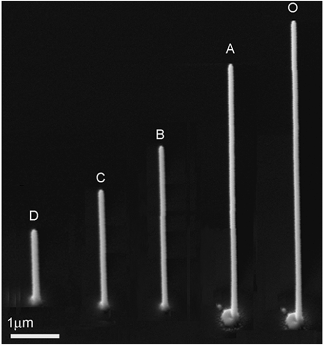
To examine the influence of the precursor gas flux, the effective supply of the reaction gas molecules was modulated by retracting the gas nozzle from the position that was optimal for maximizing the growth rate. Figure 1 shows images of rods deposited during a 5-min period using an ion beam current of 1 pA with the nozzle retracted from the optimized position O in the y–z plane in 100 μm steps to positions A, B, C, and D. A decrease of 75% is observed after retracting the nozzle by only 500 μm. This is a dramatic decrease of the deposition rate on retracting the nozzle from the region where the ion beam is scanned and suggests that retraction of the nozzle leads to substantial changes in σ in a way which is likely to be related to the detailed gas-flow dynamics within the chamber. A contrasting result was obtained previously in a report by Blauner et al.Reference Blauner, Ro, Butt and Melngailis21 on the deposition of micrometer-scale features using dimethyl gold hexafluoroacetylacetonate (C7H7F6O2Au) gas precursor; they found that, on increasing the nozzle height from about 100 to 1500 μm above the substrate surface, the deposition yield decreased only about 10%. The difference may be due to the much lower current density of 1.69 × 10⁶ e/s/μm2 (where e is the elementary charge on a Ga+ ion) that they used. For the gold deposition, since the earlier experiments were approaching the current-limited regime, from Eq. (1), the dependence of the growth rate on the gas flux would have been smaller. However, differences in the chamber design or electron optics may have contributed to the different dependence as well.
SEM sideview images of vertical nanostructures showing the effect of gas precursor nozzle position using spot mode. The substrate was tilted to 52° from the vertical for this image.

B. The effect of ion beam focusing
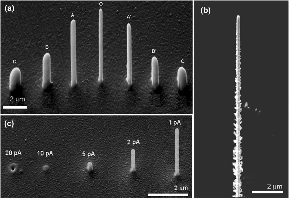
Figure 2(a) shows SEM images of nanowires deposited with different focus conditions, ranging from under-focus (−500 μm, −300 μm, −10 μm), to in-focus (0 μm), to over-focus (+100 μm, +300 μm, +500 μm). The changing of the degree of the ion beam focus was realized by first focusing the beam with the sample stage at a particular height, then lowering (raising) the stage by a certain distance ΔZ, refocussing the system, and, thereafter, moving the stage up (down) by a distance of ΔZ, thus creating an underfocus (overfocus) of ΔZ. Figure 2(a) shows that, when the beam is well focused, the rod has an almost circular cross section, with the diameter increasing with increasing defocusing level. This is easy to understand whether the cross section of the rod indicates the area over which the beam intensity exceeds a certain value that is required for efficient cracking. The asymmetry apparent in the cross section of the rods deposited away from optimal focus is likely to reflect deviations in the circularity of the beam profile related to imperfections in the electron optics such as astigmatism.
(a) SEM images of tungsten nanorods deposited in a 4-min period at various focus depths showing the influence of focusing of ion beam on nanorod growth: C (defocus = −500 μm), B (−300 μm), A (−100 μm), O (0), A′ (+100 μm), B′ (+300 μm), C′ (+500 μm); (b) 12-μm vertical platinum nanorod deposited in a 5-min period with 1 pA beam current in spot mode with optimal focus; the rough sidewall is apparent; and (c) vertical tungsten nanorods deposited in a 2-min period using spot mode and different beam currents in the range of 1–20 pA.
C. Material dependence of growth rate
Under optimized deposition conditions, vertical W nanowires with height up to a few tens of micrometers can be deposited with very smooth sidewalls with an average deposition rate of 0.025 μm3/min. For Pt nanowires, a larger growth rate of 0.100 μm3/min is obtained; however, the resulting rod diameter is typically about 1.4 times larger, and there are also substantial numbers of whiskers/branches on the sidewalls of the deposited Pt nanowires [Fig. 2(b)]. This is probably because a lower energy is required for (CH3)3Pt(CpCH3) to be cracked in Pt-composite deposition than for W(CO)6. Low-energy secondary electrons, scattered electrons, and the primary ions in the sides of the beam profile all contribute to the cracking of (CH3)3Pt(CpCH3) molecules leading to the formation of higher density whiskers and branches.
D. The dependence on ion beam current
As discussed earlier, FIB-induced deposition can be divided into two growth regions: the ion-limited growth regime and the precursor-limited regime. The deposition yield, the number of deposited atoms per incident ion, depends both on the ion beam density and gas flux. Usually, a higher ion beam density corresponds to a higher rate of precursor gas molecule decomposition. As the ion beam current is increased, more and more deposited atoms are sputtered away, and so the overall height of the grown rod is lower. For particular values of the ion beam current (for a given fixed gas-nozzle position and ion beam scanning areaReference Blauner, Ro, Butt and Melngailis21), sputtering can dominate over deposition in the center of the deposit where the ion beam density is highest, while deposition by secondary electrons and atoms dominates in the rim area where sputtering by primary ions is low or absent.Reference Chen, Veldhoven, Sanford, Salemink, Maas, Smith, Rack and Alkemade22 In such cases, a “donut”-shaped deposit with a central hole is formed. Figure 2(c) shows an example of this: the height of the grown nanowire decreases when the ion beam current was increased from 1 to 20 pA, and when a 20 pA ion beam was used, a donut was observed. These donut structures have also been observed and analyzed theoretically by Chen et al.Reference Chen, Veldhoven, Sanford, Salemink, Maas, Smith, Rack and Alkemade22 in the growth of Pt nanowires using a He ion microscope.
E. Methods for the growth of 3D nanostructures by FIB
Various methods have been used to exploit the 3D growth capabilities of FIB deposition to grow structures more complex than nanowires oriented perpendicular to the substrate. In this section, we review the two major options available: tilting the stage before deposition and shifting the beam during deposition.
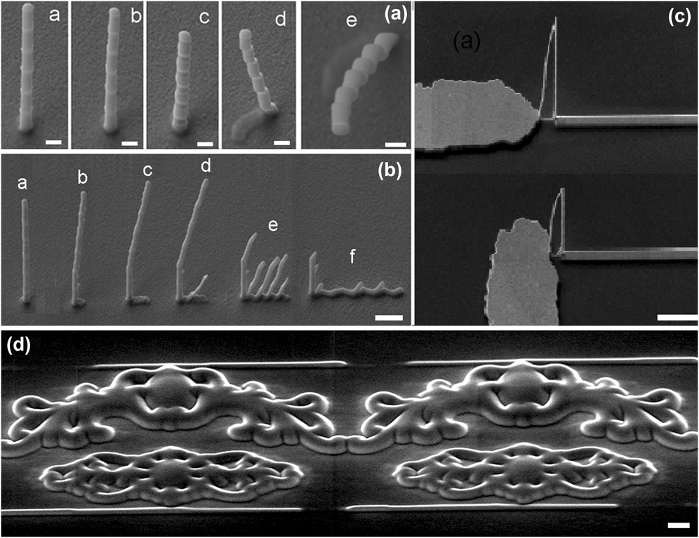
The simplest possibility is to tilt the substrate with respect to the incident ion beam before starting growth. Figure 3(a) shows freestanding structures deposited by tilting the stage while keeping the gas nozzle and the direction of the incident ion beam fixed; these structures have a “bamboo-like” appearance. This is because a rectangle pattern was used with the ion beam scanned in a meander mode (the ion beam scanned from +Y to −Y and then −Y to +Y), so deposits built up both on the vertical and lateral directions as the beam moved each step in the Y direction. Since, however, it is necessary to have the gas injection nozzle in close proximity to the substrate surface (particularly for growth at 1 pA), there is a geometrical constraint on the maximum possible tilt of the substrate. This means that only very simple structures can be grown by tilting the stage alone.
Methods for complex structure growth: (a) freestanding bamboo-like structures grown with stage tilting [the stage-tilt angle for (a)–(e) is 52, 42, 32, 22, 0°, respectively]; (b) flying tungsten fabricated making use of ion beam nudging with r of 0.1 m and (a) no nudging, and t of (b) 30 s, (c) 12 s, (d) 10 s, (e) 6 s, and (f) 3 s; (c) tungsten air-bridge structures; (d) 2.5D crown flower using a grayscale bitmap file. Images were taken with a viewing angle of 52° and the scale bar is 1 μm.
For more flexible 3D fabrication by FIB-induced deposition, beam shifting can be used. Here, the position of the ion beam is shifted during the deposition, which may be carried out while keeping the ion beam normal to the substrate surface. The process typically involves: (i) deposition of a vertical section on a substrate with the beam position fixed; (ii) repeatedly nudging the ion beam position by a distance Δr followed by deposition for a duration Δt at this point, until a structure of the desired geometry has been grown. For particular deposition conditions, the local angle of deviation (α) of the growth vector of the 3D structure being grown from the vertical can be controlled by choosing Δr and Δt Reference Li and Warburton18: For a given growth rate and fixed Δr, α increases with decreasing Δt. (At the same time, debris also deposited on the substrate below increases.) As the deposition proceeds, in each pass the new-grown material extends a little more over the side of the feature while the rest is deposited on the substrate to form the debris. For small nudging rates Δr/Δt, a linear dependence of local tilt angle α on 1/Δt was observed. This suggests that under certain ion beam operating and deposition conditions, it is possible, technically, to control the local tilt angle α within a certain range. For instance, for features with a target cross-sectional area of 130 × 130 nm2 and an average vertical growth rate of 16 nm/s, the minimum tilt angle obtained is 66.6°(±0.5°).Reference Li and Warburton18
For concrete applications based on this simple principle of ion beam nudging/shifting, powerful software has recently been developed for controlling the scanning of the ion beam to generate multilayered patterns and to control the alignment accuracy of these patterns. For instance, the Nanobuilder software installed on a FEI Helios 600i system (Portland, OR) can be used to fabricate 2D and 3D structures. With it, sophisticated patterns can be designed and used to guide the scanning of the ion beam to write the desired pattern; moreover, the ion dose can be adjusted to deposit each layer of material with a desired size, and thus to build up a 3D structure such as the one shown in Fig. 3(c). Bitmap patterns, e.g., can also be used with such software and these enable the fabrication of bespoke complex structures. In this method, the intensity at each pixel in the bitmap pattern determines how long the beam dwells at a particular point on the surface and therefore how thick the deposit is at that point. Figure 3(d) shows a 2D crown flower produced by FIB-induced deposition of platinum utilizing a grayscale bitmap file.
F. Structural and compositional properties
FIB-CVD-deposited nanowires are not single-element materials but also contain some gallium, carbon, and oxygen. Chemical composition analysis of freestanding nanowires was carried out by energy dispersive x-ray spectroscopy and electron energy loss spectroscopy installed in a transmission electron microscope (TEM). To accomplish this, vertical nanorods were grown on a holey-carbon TEM grid attached onto a SEM sample holder. After growth, ultra-low-current FIB milling was conducted with the ion beam normally incident on the TEM grid to cut through the carbon networks around the base of a nanowire. Once its support was removed, the rod fell down, lying on the holey-carbon TEM grid, which was then transferred to the TEM chamber for further chemical composition and structural examination. Vertically grown tungsten rods deposited with 1 pA ion beam current were found to have respective atomic concentrations of W, C, Ga, and O (at.%) of approximately 42:40:12:6. High-resolution TEM imaging of a vertical rod shows the absence of long-range crystalline order. Inspection of the image at a higher magnification shows the possible presence of nanocrystallite clusters with size of the order of 1 nm, similar to those in laterally grown nanowires deposited using the same ion beam current.Reference Li, Fenton, Cui, Wang, Wang, Gu, McComb and Warburton23 Thus, both in terms of its composition and its structure, FIB-deposited “tungsten” is very different from crystalline tungsten.
G. Electrical properties
Bulk tungsten has a resistivity of 5 μΩ cm at room temperature. Resistivity values from about 100 to 300 μΩ cm have been reported for lateral W composites grown by FIB-CVD.Reference Ross, Luxmoor, Cullis, Orr, Buckle and Jefferson16 In general, a variation in the resistivity of the FIB-deposited materials is a consequence of the microstructure and composition due to the operating parameters, e.g., the ion beam current, dose, substrate material, substrate temperature, scan speed, and gas flux. To obtain high aspect ratio freestanding nanowires, the lowest ion beam current is usually used for deposition.
To measure the resistivity of a freestanding nanowire, after the growth the wire was felled by lateral ion beam milling following the approach reported previously.Reference Li, Fenton, Cui, Wang, Wang, Gu, McComb and Warburton23 After this, a four-terminal configuration [Fig. 4(a)] was formed, and the I–V curves were measured by a probe system. Using the size measured by SEM imaging, the electrical resistivity of tungsten nanowires was calculated to be around 500 μΩ cm. Similarly, for the 3D air-bridge structure [Fig. 4(b)], after growth the debris underneath was removed and then an I–V measurement was made. The resistance of the leads was found by subsequently knocking down the air-bridge structure, depositing a strip to bridge the gap and then taking another I–V measurement. From the difference between the two resistances, the resistivity of the 3D structures could be determined; this was found to be about 550 μΩ cm; more details can be found in Ref. Reference Li, Fenton, Cui, Wang, Wang, Gu, McComb and Warburton23.
SEM images (with a viewing angle of 52°) and temperature dependent normalized resistivity of tungsten structures on SiO2/Si substrate: (a) four-terminal configuration on a felled vertical nanwire; (b) 3D tungsten air-bridge after debris removal; (c) the ρ-T of the felled nanowire; and (d) the ρ-T of the air-bridge structure.
The superconducting properties of the vertical tungsten nanowire and the flying air-bridge structures were measured using a quantum design physical properties measurement system with temperature sweeping from room temperature down to 1.8 K. Figures 4(a) and 4(b) show typical SEM images of the four-terminal structures formed on a felled vertical nanowire and for a flying tungsten structure. For the four-terminal configuration, a constant current of 1.0 μA was applied to the two outer terminals and the voltage was measured between the other two terminals as shown in Fig. 4(a). The transition temperature observed for the felled vertical nanowire (measured in a four-terminal configuration) is similar to that observed for the 3D air-bridge structure (albeit measured in a two-terminal configuration), as shown in Figs. 4(c) and 4(d). This confirms that vertically grown tungsten nanofeatures have transition temperatures above 5.0 K. This is noticeably much higher than that of single-crystal tungsten, which has a very low transition temperature: T c of alpha (bcc) W is 15 mK and that of beta (A15) W is in the range 1–4 K. The mechanism behind this enhanced superconductivity of FIB-deposited tungsten is discussed elsewhere.Reference Li, Fenton, Wang, McComb and Warburton24
III. 3D NANOSTRUCTURES BY FIB-IRRADIATION-INDUCED PLASTIC BENDING
Although FIB-induced deposition of complex structures using beam shifting offers great flexibility and controllability in producing 3D conducting micro/nanostructures that can be used as freestanding electrodes, there is undesirable, but unavoidable, deposition near the structure as a result of secondary electron and ion generation; the debris may cause contamination or provide extra conduction path. Recently, more and more attention has been paid to a bottom-up approach involving the construction of freestanding 3D nanostructures and nanodevices with bending of nanowires by ion beam irradiation. This may provide an alternative technique that can be utilized to produce freestanding and electrically conducting nanostructures without unwanted deposition on the substrate surface.Reference Romans, Osley, Young, Warburton and Li5 Previous study of ion-beam-irradiation-assisted bending has been conducted on nanowires of various materials, including carbon,Reference Morita, Kometani, Watanabe, Kanda, Haruyama, Hoshino, Kondo, Kaito, Ichihashi, Fujita, Ishida, Ochiai, Tajima and Matsui6 dielectric,Reference Arora, Sijbrandij, Stern, Notte, Smith and Barbastathis25 metallicReference Xia, Wu, Xu, Hao and Wang26 and semiconductingReference Jun, Joo and Jacobson27 nanowires, nanotubes, and cantilevers. A range of different bending behaviors have been observed and related bending mechanisms have been proposedReference Morita, Kometani, Watanabe, Kanda, Haruyama, Hoshino, Kondo, Kaito, Ichihashi, Fujita, Ishida, Ochiai, Tajima and Matsui6,Reference Arora, Sijbrandij, Stern, Notte, Smith and Barbastathis25–Reference Jun, Joo and Jacobson27 taking into consideration parameters such as the kinetic energy, mass, fluence, and incident angle of the ion beam. Only very recently has attention also been given to the possible effect of Coulomb interaction and the role of the substrate.Reference Cui, Fenton, Li, Shen, Liu and Gu28 In the Sec. III. A, systematic experiments we have carried out into nanowire bending are reviewed, and our analysis based on Coulomb interactions with charge deposited on the substrate is shown to broadly explain the observations.
A. Bending trends
To develop a technology for controllable shape manipulation of freestanding nanowires using ion beam irradiation, the general ion-beam-induced bending behavior of nanowires was first explored. Vertical nanowires with various heights were grown on Si and Al substrates by FIB-induced deposition using a 1 pA ion beam current. Groups of, or individual, nanowires were then irradiated with ion beam currents in the range of 30–100 pA with ion energy of 30 keV, and the influence of the ion beam current and the ion incident angle on the bending were systematically investigated. After each irradiation scan, the stage was tilted to 45° off normal to the electron beam to enable observation of the bending by in situ SEM.
The ion beam scanning strategies, raster scanning, and reduced raster scanning, used for bending manipulation, are illustrated in Figs. 5(a) and 5(b). The definitions of the incident direction of the irradiation ion beam (β), which is the angle between the incident ion beam and the long axis of the wire, and the bending angle (ф), the angle between the vertical of the substrate and the long axis of the wire, are illustrated in Figs. 5(c) and 5(d), respectively.
Schematic illustration of (a) the raster scanning process, (b) reduced raster scanning, (c) the definition of the ion beam incident angle, and (d) the bending angle of the nanowire.
Figures 6(a) and 6(b) show SEM images of the as-deposited and irradiated nanowires grown on Al and Si substrates, respectively. The corresponding bending angle as a function of the ion sweep number is shown in Figs. 6(c) and 6(d). It can be seen that from Figs. 6(c) and 6(d) that on both the Si and Al substrate, the bending occurs toward the incident ion beam until the wires become parallel to it. Once the nanowire is parallel to the incident ion beam, the bending angle saturates, similar to previous reports of the bending of a range of different nanoobjects.Reference Arora, Sijbrandij, Stern, Notte, Smith and Barbastathis25–Reference Jun, Joo and Jacobson27
Bending of vertical nanowires: (a and b) SEM images show the bending process of tungsten nanowires grown on Al and Si substrates; (c and d) the bending angle as a function of the ion sweep number; (e) the ion beam incident angle dependent bending angle; and (f) the influence of the ion beam current.
The dependence on the incident angle of the ion beam was examined with groups of identical nanowires. The stage was tilted to change the ion beam incident direction, and raster scanning was carried out using an ion beam current of 100 pA. Figure 6(e) shows the ion-beam-incident-angle dependence of the bending of tungsten nanowires (around 2.3 μm in height and 60 nm in radius) occurring at the initial irradiation stage, for ions incident at angles of 10, 30, and 50° with respect to the vertical. Again, the wires bent until they became aligned with the ion beam direction. The nanowires bent further per scan when irradiated from a larger ion beam incident angle. This is as expected since the larger the ion beam incident angle, the larger the number of ions interacting with the sidewall of a nanowire per scan. The influence of the ion beam current is shown in Fig. 6(f). Using a higher ion beam current, fewer scans are required for a nanowire to bend to a certain angle compared with using a lower irradiation ion beam under otherwise identical conditions.
Figure 7 presents the results of similar experiments performed on Si nanowires, which were fabricated by inductively coupled plasma etching; similar bending behavior was found. Again, raster scanning the ion beam across the nanowires caused them to bend gradually toward the ion beam and finally to align with the ion beam, as shown in Fig. 7(a). By adjusting the stage rotation, the bending direction with respect to the edge of the substrate can be changed [Figs. 7(b) and 7(c)]. In addition, by increasing the field of view, arrays of nanowires can be bent in one ion sweep, as shown in Fig. 7(d). These results indicate that FIB-irradiation-induced bending could be used to fabricate structures in an area sufficiently large to have practical applications.
FIB-irradiation-induced bending of Si nanowires: (a) gradual bending with increased ion sweep number (from left to right); (b and c) changing of the bending direction by state rotation; and (d) bending of an array of nanowires. The scale bar is 1 μm.
B. Dependence on the supporting substrate
The influence of the underlying substrate on the bending of FIB-grown W nanowires was further studied with tungsten nanowires grown on SiO2 (200 nm)/Si substrates with isolated Au pads previously formed on it. The Au layer was about 65 nm thick, and each pad had an area of 30 × 30 μm. Freestanding nanowires with height of 3.0 μm were grown on the Au pads, which were not grounded during ion beam irradiation. Figure 8(a) shows typical SEM images indicating the changes caused by successive ion sweeps. As presented earlier, nanowires grown on Al and Si substrates initially bent toward the ion beam, and after sufficient ion beam irradiation, aligned with the ion beam. In contrast, when Au/SiO2/Si substrates were used, the W nanowires (which had a radius of around 105 nm) first bent away from the ion beam before bending back toward the ion beam and finally aligning with the ion beam [Fig. 8(b)]. It can also be seen from Fig. 8(b) that the Au pad on the substrate is gradually removed during the ion irradiation.Reference Cui, Fenton, Li, Shen, Liu and Gu28
Bending of FIB-grown W nanowires grown on isolated 30 μm2 Au pads (30 nm thick) on SiO2(200 nm)/Si substrates: (a) SEM images and (b) the bending angle as a function of the ion beam sweep number. The ion beam current was 47 pA. The scan covered an area 15.2 × 13.1 μm2 on the substrate and took 163 s. The scale bar is 1 μm; the lines are guides to the eye.
C. Effect of the beam scanning strategy
The bending trajectory of a nanowire can be influenced by changing the position of the ion beam scanning area with respect to the nanowires being irradiated. Using reduced raster scanning or by moving the sample stage, a nanowire can be placed in the center or at one side of the ion beam scanning area. The sample position was extremely carefully adjusted to lie at the coincident point, the point at which the SEM and FIB beams cross. Figures 9(a) and 9(b) illustrate the relative position of the incident ion beam to the nanowires. X and Y label the perpendicular directions in the substrate plane; the ion beam is directed toward the nanowire from an angle above the +Y axis.
Scanning-strategy-dependent bending phenomena: (a and b) schematic diagram illustrating the relative position of the nanowire to the incident ion beam; and (c) bending images of W nanowires grown on SiO2/Si substrates taken on successive sweeps indicate bending in both +Y (−Y) and +X (−X) directions for wires near the edge of the ion beam scanning area. The electron beam scans from −X to +X and from +Y to −Y. Note that the ion beam scans are from +X to −X and from −Y to +Y.
It was found that, for nanowires grown on Al and Si substrates, when a sufficiently high ion dose was used, bending occurred only along the +Y direction (toward the incident ion beam). However, when the nanowire was standing on an insulating substrate, a bending component in the −X or +X direction could also arise, dependent on the relative position of the nanowire within the ion beam scanning area [shown in Fig. 9(b)] and also on the scanning speed: when a 150 pA ion beam was scanned rapidly across an area of 15.2 × 13.1 μm2, taking 163 s for a complete scan, no obvious bending along the +X or −X direction was observed: these wires only bent along the −Y and +Y directions. In contrast, when a faster ion beam scan was made in the same area, taking 6 s for a single scan, bending with a component in the −X or +X direction was observed, as can be seen from the SEM images taken on successive ion sweeps over a group of three nanowires shown in Fig. 9(c). Bending in the direction normal to the incident ion beam is clearly seen. In detail, the nanowire at the left edge (L) of the irradiated area initially bent toward the −X, −Y quadrant; when the wire was in the center (C) of the ion beam scanning area, it first bent along −Y and then bent back along +Y and finally aligned with the incident beam. When the nanowire was on the right side (R) of the ion beam scanning area, it first bent toward the +X, −Y quadrant, then to the +X, +Y quadrant and finally aligned with the ion beam. In Sec. III. D, we develop a framework for explaining this bending behavior.
D. Bending mechanism
The bending observed in W nanowires grown on Au/SiO2/Si substrates, first bending away from and then toward the ion beam, is similar to the observations reported on crystalline Si and Ge nanowires on Si substrates.Reference Ross, Luxmoor, Cullis, Orr, Buckle and Jefferson16,Reference Matsui, Kaito, Fujita, Komuro, Kanda and Haruyama17 In these works, the effect was explained by a gradually amorphization, starting from the side facing the ion beam and moving across the wire until reaching the far side. However, W nanowires deposited by FIB-CVD are amorphous in nature as-grown and therefore the same explanation cannot apply to them. Using exactly the same irradiation conditions (beam current, scanning strategy, relative location of nanowire with respect to the incident ion beam), the difference in bending behavior for nanowires (deposited using identical conditions) grown on substrates with differing surface conductivity is suggestive of the importance of charging. In support of this, in Fig. 9, it can be seen that the only clear differences between the situations of the wires on either sides of the scan area, but showing opposite behavior, are most likely to be charge related. The nanowire becomes positively charged as a result of irradiation by the positively charged ion beam and the substrate also becomes positively charged. When these charges persist, there is a net force on the nanowire away from the center of the ion line scan, leading to bending in the direction observed in Fig. 8. The symmetrical behavior between wires scanned toward the left edge of the scan area and those scanned toward the right edge of the area implies that the behavior is not determined by a force between the charged ion beam itself and the nanowire. The features of the observed results suggest that the bending process described above is very likely mediated by the electrostatic forces. A 30 pA, 30 keV ion beam contains at any instant ∼1 ion per millimeter; thus electrostatic forces involving the ion beam itself are not important.
Although bending due to electrostatic forces may be elastic initially, the persistence of the bends after the ion scan has finished shows that they become plastic at some stage, most likely during or shortly after the ion beam strikes the nanowire.Reference Chen, Veldhoven, Sanford, Salemink, Maas, Smith, Rack and Alkemade22 It is likely that the energy deposited in the wire in collisions leads to structural changes in the vicinity of the collision site which relax strain in the wire and tend to fix the bend in the nanowire, corresponding to an increased (decreased) likelihood of material ending up in regions of tensile (compressive) strain.
The observed elastic bend of a nanowire as a result of the electrostatic forces has been investigated based on a simple model. In this model, charge deposited on the substrate leaks away over some time characterized by the conductivity of the substrate surface.Reference Cui, Fenton, Li, Shen, Liu and Gu28 For a substrate with sufficiently low surface conductivity, the charge deposited on the substrate may be considered as a line charge. The net force on these charges in directions perpendicular to the nanowire leads to a transverse deflection d which may be determined from the theory of bending beamsReference Chen, Alkemade and Salemink29 as
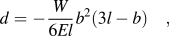 $$d = - {W \over {6El}}{b^2}(3l - b)\quad ,$$
where W is the net transverse force and b is the distance from the base of the nanowire (of length l, Young's modulus E, and area moment of inertia I).
Therefore, a net deflection which depends on the location of the line charge with respect to the nanowire can be calculated, taking E = 150 GPa,Reference Bret, Utke, Hoffmann, Abourida and Doppelt30 the wires to be of circular cross-section, neglecting secondary electron emissionReference Blauner, Ro, Butt and Melngailis21 and allowing charges to move along the nanowire in response to both the external electrostatic force and the mutual repulsion between deposited charges. Thus, the deflection of the wire resulting from a single linescan depends on the location of the wire along the linescan and on the height above the base at which the ion beam strikes the wire. The nanowire deflects away from the center of the linescan and by a greater amount further away from the center of the linescan. This is just what was observed in the experiments with insulating substrates and the same order of magnitude. The deflection increases in proportion to the number of linescans for which charge persists on the substrate. The difference in bending behavior between fast and slow scans suggests that this timescale for charge to leak away is ∼10–100 ms.
This electrostatic force also has a component in the +Y direction. Based on the model described above, the deflection is found to be of the same order of magnitude as the transverse bending and is largest when the nanowire is close to the center of the linescan and for linescans around halfway up the nanowire; this is associated with the directionality and the fall-off trend of the electrostatic interaction. We note that, in principle, field emission of electrons in the associated electric field will occur; however, a simple estimation suggests that the magnitudes of the electric fields involved here are orders of magnitude smaller than would lead to a significant field-emission current.
In the case of a conducting substrate, charge deposited on either the wire or on the substrate leaks away rapidly. Thus, the magnitudes of the electrostatic forces at least are much smaller than for insulating substrates. For the Au nongrounded isolated pad on SiO2/Si substrate, before the Au layer is fully removed, the charge accumulated on the Au pad can quickly distribute itself uniformly over the pad. As a consequence, a net electrostatic force bending the nanowires away from the center of the pad is expected. The model of electrostactic interaction cannot explain why the wires eventually have the tendency to bend toward the ion beam direction. However, the ion modification of the surface of the wires that exposed to the ion beam, which could produce a compressional strain, has also been observed by other research groups.Reference Koshnick, Huber, Bert, Hicks, Large, Edwards and Moler31 As previously reported, the energy, the dose, and the species of ions, together with the size of the irradiated object, are the main factors that determine the difference in the changes of the volume or stress distribution on the two sides of the wires (facing and opposite the incident ions). In some cases, the wires may first bend away from the ion beam but, with long enough ion irradiation, wires will finally align with the incident ion beam, minimizing the area of interaction so that only mild milling occurs, at the top facet of the object. While the precise mechanism for such a plastic deformation that “homes in” on the direction of the ion beam is not clear, the change in the bending direction of the wires on the gold pads seems to coincide approximately with the removal of the gold layer and subsequently the SiO2 insulating layer; after this, the wires are on a conductive substrate and the accumulation of charge on the surface is no longer significant.
Furthermore, momentum transfer of the ions to the beam leads to a force away from the ion beam. The magnitude of the force on the wire due to momentum transfer should cause to a deflection of the wire ∼1 nm. If a substantial proportion of this bend is fixed into the wire on each linescan, the total bend might reach several tens of nanometers, large enough to explain the bending away from the beam. Obviously, the electrostatic interaction alone cannot produce a plastic deformation, so the role of the ion beam in providing local heating/annealing and structural modification is pivotal. The modification of the exposed area of the wire surface layer by the ion beam is also a significant factor. Nevertheless, a careful calibration of processing parameters is likely to make the electrostatic-mediated ion-beam-induced nanowire bending a practical tool for postgrowth nanoscale manipulation.
E. Construction of compound 3D nanostructures
Figure 10(a) shows schematically a process for constructing 3D nanocontacts, multibranched structures, and nanogaps by FIB-induced deformation of vertically grown nanoobjects. To guide the bending process and control the ultimate shape of the new structures, the optimized stage-tilting angle can be found based on the heights and interspacing of nanowires to be irradiated. For instance, for a freestanding joint contact between two vertically grown nanowires, W1 and W2, and denoting the heights of the respective nanowires as h 1 and h 2, and the spacing between them as d, the steps include: first, the stage is rotated to bring W1, W2, and the ion beam into the same line, with W2 nearer to the ion beam than W1; then, the stage is tilted with a tilt angle of θ; after setting the experimental geometry, the ion beam is scanned in reduced raster mode; on irradiation, the nanowire W2 bends toward W1 and forms a contact at the top of W 1 when the stage-tilt angle and the height and spacing of the two wires meets the following conditions:
 $$\theta = {\rm{arc \;tan}}\left( {{{h_1 } \mathord{\left/ {\vphantom {{h_1 } d}} \right. \kern-\nulldelimiterspace} d}} \right)\quad ,$$
 $$h_2^2 \;\ge\; h_1^2 + {d^2}\quad .$$
Freestanding tungsten nanostructures formed from FIB-grown tungsten nanowires: (a) schematic of construction of joint-nanocontacts/nanogaps by FIB-induced deformation of vertically grown nanowires; (b) SEM image of pairs of joint-contacts; (c) nanogapped structures; and (d) multibranched structures. The scale bar is 1.0 μm.
Figure 10(b) shows an example of the use of this process, with a joint nanocontact formed between two pairs of tungsten nanowires with heights of 2.8 and 1.5 μm, and interspacing of 2 μm. The wires were grown on a SiO2/Si substrate by FIB-induced CVD. To make the nanocontact, the stage was rotated to bring W1, W2, and the ion beam into the same line and after this, with the stage tilted at 36°, reduced raster scanning was performed to irradiate one row of nanowires so that they bent toward the incident ion beam and finally made contact with the as-grown nanowires on the other row. Figures 10(c) and 10(d) show that nanogaps with tunable distance can also be formed by adjusting the stage rotation angle, the ion beam incident angle (changed by the tilting the stage), and the size and interspacing of the as-grown nanowires. More complicated multibranched structures and cross-contacted/gapped structures can be formed by performing stage rotation and tilting repeatedly to manipulate the leaning direction of different wires in combination of irradiating a portion of a nanowire. These results demonstrate that freestanding 3D nanostructures in various geometries can be formed with nanometer-range precision.
The conducting and superconducting properties of bent air-bridge nanostructure were measured from room temperature down to 1.8 K. The normal-state resistivity was found to be around 300 μΩ cm, and the superconducting transition temperature was about 5.1 K. These values are similar to those for as-deposited nanowires. The current density is measured to be in the order of 104 μA/μm2. This confirms that the technique of FIB irradiation can be used to form freestanding superconducting nanostructures with clean, smooth, and uniform size as well as reliable superconductivity and mechanical properties.
IV. POTENTIAL APPLICATIONS OF FIB-PRODUCED 3D CONDUCTING NANOSTRUCTURES
It has been demonstrated that the freestanding nanoscale features grown by FIB are conducting; this is essential for fabrication of functional electrical devices. Low-current FIB deposition may be used, together with the flexibility of site-specific growth and 3D structuring, to fabricate nanoelectrodes/3D wiring for making nanocontacts to freestanding nanomaterials, e.g., as electrodes for contacting the vertical leg of ZnO and CdS tetrapod nanocrystals.Reference Morita, Kometani, Watanabe, Kanda, Haruyama, Hoshino, Kondo, Kaito, Ichihashi, Fujita, Ishida, Ochiai, Tajima and Matsui6
In addition, their properties, such as the much enhanced superconducting transition temperature and the amorphous microstructure of the FIB-grown features, suggest applications such as mask-free superconducting devices, including superconducting nanomechanical resonators for studies of macroscopic quantum phenomenaReference Stanishevsky, Edinger, Orloff, Melngailis, Stewart, Williams and Clark14 and compact vertical inductors for high-frequency environmental isolation of superconducting qubits.Reference DeMarco and Melngailis15 Among these applications, 3D SQUIDs can be formed by integration of freestanding multiple pickup loops with conventional planar SQUID and these could potentially overcome a limitation of conventional SQUIDs that only detect the field perpendicular to the substrate. Such a device can be used to detect different field components (B x, B y, and B z) or field gradients ( $\partial Bi/\partial j$, where i,j = {x,y,z}) with single-spin resolution.Reference Romans, Osley, Young, Warburton and Li5
Furthermore, micro/nanoobject immobilization has been intensely studied and this has potential applications in bioscience,Reference Hegner, Dreier, Wagner, Semenza and Güntherodt32quantum optics,Reference Gaur, Koktysh and Weiss33 and optical trapping.Reference Neuman and Block34 With dedicated design, bird-cage nanostructures can be formed. Such enclosures fabricated using the tungsten superconducting composite nanowires through ion-irradiation-induced-bending are size-controllable. Not only this, but they also show favorable conductivity and superconductivity. They could potentially be used for volume-selective entrapment of magnetic and optical beads, particles, and macromolecules.Reference Bopp, Sytnik, Howard, Cogdell and Hochstrasser35
V. CONCLUSION
In conclusion, the direct growth of freestanding conducting and superconducting 3D nanostructures, and the postgrowth shape manipulation of 1D freestanding amorphous nanowires using FIB irradiation to construct 3D nanostructures, based on the techniques of FIB-CVD and FIB irradiation, have been systematically investigated and reviewed in this article. The results reveal that (1) the growth of nanoscale freestanding nanowires with high aspect ratio is strongly affected by parameters such as the precursor gas flux, the current density, and the focusing of the ion beam; (2) FIB irradiation can be used to manipulate the shape of freestanding 1D nanoobjects, the bending behavior is highly reproducible and controllable, depends on the ion beam scanning strategy and also on the conductivity of the supporting substrate, suggestive of the role of electrostatic interaction in the mediation of the ion-irradiation-induced nanowire bending behavior; (3) the formed 3D tungsten nanostructures are conducting and superconducting with much enhanced superconductivity compared with their bulk counterparts. All these results suggest that FIB techniques—direct wiring or postgrowth shape manipulation—can potentially be used to fabricate versatile building blocks for free-space multifunctional nanodevices, such as one-node multibranch 3D functional units, freestanding electrodes, wiring, and nanoswitches, especially in the construction of superconducting devices with performance that cannot be achieved by planar devices, e.g., fabrication of multiple loops in 3D toward the measurement of different field components or field gradients.
ACKNOWLEDGMENTS
The authors would like to acknowledge helpful conversations with Huan Wang and Dr. Grenville Jones and Professor Philip Grundy. This work is supported by the Technical Talent Program of the Chinese Academy of Sciences, the National Natural Science Foundation of China under Grant Nos. 91123004, 11104334, and 51272278, and the National Basic Research Program (973) of China under Grant No. 2009CB930502.