Introduction
Although it all started in the 1970s with thin-film electroluminescent displays,Reference Suntola1 it was only recently that atomic layer deposition (ALD) found several mainstream applications, mostly in the semiconductor and related industries.Reference Ritala and Niinistö2 For example, ALD is used in the manufacturing of magnetic read-write recording heads,Reference Paranjpe, Gopinath, Omstead and Bubber3 in high-κ dielectric deposition in 3D capacitors for dynamic random-access memory (DRAM) technology,Reference Kim, Choi, Lee, Seo, Lee, Han, Ahn, Han and Hwang4 and in gate-stack formation of logic devices.Reference James5 For these applications, ALD processes use conventional metal oxide thin-film materials (particularly Al2O3, HfO2, and ZrO2-based) and are based on the thermally driven ALD surface chemistry of halide and metal-organic precursors with H2O. For practical applications, the processes are initially also mostly explored and introduced as single-wafer processes, although multiple-wafer batch processes have been implemented for DRAM technology.
Among the many novel applications that could benefit from thin films prepared by ALD, several will depend on new and even disruptive process technologies to extend the capabilities of ALD in order to make them technologically feasible and economically viable. New process technologies can be required for a large variety of reasons, such as the need for low-temperature processing, the preference for bottom-up patterning capability, the use of flexible, large-area or other non-wafer-like substrates, and the necessity for fast and/or high-throughput processing. These novel applications are likely to be seen first within the fields of nanoelectronics, photovoltaics, and flexible electronics. They constitute large, expanding markets in which cost reduction is a main driver and with each of them having its particular challenges (i.e., miniaturization, high-throughput processing, and substrate material handling, respectively).
In this article, some recent developments are presented in which ALD processes and applications expand beyond single-wafer semiconductor processing with conventional thermal ALD. As advanced process technologies rely heavily on innovative, new reactor, and processing concepts that are often not reported in the open scientific literature due to business reasons, this overview is not intended to be historical and exhaustive. The aim is merely to illustrate how innovations within the field of ALD can contribute to the integration of viable manufacturing schemes with the benefits of ALD thin-film processing.
Beyond single-wafer thermal ALD
The most common type of ALD reactor is a single-wafer thermal ALD reactor in which ALD cycles are carried out in the time domain. This means that precursor and reactant (here the term “reactant” instead of “second precursor” is used for the agent that leads to oxidation or reduction of the growth surface) pulsing as well as the intermediate purge steps are carried out subsequently in time. For a well-optimized reactor and process, the cycle time can be below 1 s. Single-wafer ALD reactors are generally used for processes requiring extremely tight process control such as in transistor gate stack formation. They are also used in most R&D studies as well as in the pre- or early production stage for most applications. So far, mostly metal oxide films have been deposited by ALD, with H2O being the common reactant, although O3-based processes are gaining in popularity quickly. Ozone-based ALD processes are considered due to the fact that O3 allows for a wider selection of precursors, including those with enhanced thermal stability, and because purge times can be significantly shorter compared to H2O-based ALD in some cases.
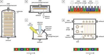
One of the main drawbacks inherent to a single-wafer ALD reactor is the relatively low throughput of the system. Depending on the process, the material, and the film thickness required, a single-wafer reactor can, at a maximum, process several tens of wafers per hour, but this holds only in cases in which film thicknesses are less than 10 nm. For thicker films and many material systems, the ALD process times are typically longer than a few minutes. This holds also in cases where films have to be deposited in high-aspect-ratio structures. In these cases, single-wafer ALD is often incompatible with the needs for high-volume manufacturing. To mitigate the low throughput of ALD, interest in batch reactors has rapidly expanded. In a batch reactor, typically up to 100 wafers (or other substrates) can be processed at a time (see Figure 1a).Reference Granneman, Fischer, Pierreux, Terhorst and Zagwijn6 Already, during early applications of ALD, batch reactors were investigated and employed in the manufacture of thin-film electroluminescent displays (to synthesize films with thickness >1 μm);Reference Putkonen7 however, the DRAM industry has been the main driver for batch ALD. In advanced DRAM technology nodes, ALD processes are inevitable due to the required high conformality of the films.Reference Kim, Choi, Lee, Seo, Lee, Han, Ahn, Han and Hwang4 Moreover, the demands on throughput and cost of ownership performance per wafer are much tighter than for logic applications.
Different atomic layer deposition (ALD) process technologies: (a) batch ALD;Reference Granneman, Fischer, Pierreux, Terhorst and Zagwijn6 (b) plasma-enhanced ALD;Reference Heil, van Hemmen, Hodson, Singh, Klootwijk, Roozeboom, van de Sanden and Kessels8 (c) direct-write ALD combining a nanopatterning technique such as electron- or ion-beam-induced deposition with ALD;Reference Mackus, Mulders and Kessels22 (d) spatial ALD;Reference Levy, Freeman, Nelson, Cowdery-Corvan and Irving24, Reference Levy, Nelson and Freeman25 and (e) roll-to-roll ALD.Reference Dickey and Barrow37 In (a)–(c), the ALD cycles are carried out in the time domain (t, time), and (d) and (e) are in the spatial domain (x, position). The precursor step is labeled “A” and the reactant step “B.” The precursor and reactant steps are separated by purge steps.

ALD processes, however, do not always behave ideally, despite the uniform films achieved on R&D size substrates. When batch sizes are scaled up, small variations in the growth rate or slight thermal decomposition of the precursors can be detrimental to the resulting film. Careful process tuning is therefore often necessary to amend the deviations in the process. Moreover, due to the large amount of precursors required in a batch process, high evaporation rates are often needed, requiring higher evaporation temperatures. This severely limits the ALD chemistries that can be employed in batch reactors. Furthermore, several materials, processes, and applications pose different demands on the ALD process than that reflected in the choice between single-wafer or batch reactor. In particular cases, ALD processes can benefit from or even require additional reactivity over the energy provided thermally. In such cases, energy-enhanced ALD processes can be employed, for example, ALD processes assisted by plasma activation (see Figure 1b). Moreover, in the wider sense of the word, ALD processes assisted or enabled by energetic particle beams can be considered to be “energy-enhanced.” An example of this is the so-called direct-write ALD technology combining electron-induced or ion-induced deposition with ALD (see Figure 1c). Other applications require spatial-ALD schemes in which the ALD cycles are not carried out in the time domain but in the spatial domain. This means that the precursor and reactant are continuously injected at different positions using distinct reaction zones separated by purge zones. In this case, either the substrates or an “ALD deposition head” are moved such that the substrate surface area is alternately exposed to different reaction zones (see Figure 1d). Spatial-ALD schemes implemented in inline deposition systems are expected to be inevitable when extremely high throughputs are required with low cost-of-ownership. In these cases, ALD processes are preferably operated at atmospheric pressures, enabling gas barriers to separate the reaction zones and avoiding expensive vacuum equipment. Another example showing the demand for spatial-ALD schemes is roll-to-roll processing, in which flexible foils (webs) act as substrates (see Figure 1e). The energy-enhanced and spatial-ALD configurations are discussed in more detail next.
Plasma-enhanced ALD
Plasma-enhanced ALD processesReference Heil, van Hemmen, Hodson, Singh, Klootwijk, Roozeboom, van de Sanden and Kessels8, Reference Profijt, Potts, van de Sanden and Kessels9 differ from thermal ALD processes by the fact that during the reactant exposure step, plasma excitation is used to create reactive vapor species that impinge on the growth surface. Such species can comprise charged plasma species such as electrons and ions but also neutral gas species, which can be internally excited or by any other means reactive (generally labeled “radicals”). The plasma is generated in a plasma source that uses electrical power to ionize and dissociate the gas introduced, typically O2, H2, N2, NH3, or mixtures thereof. A variety of plasma sources as well as different plasma-enhanced ALD configurations exist. For example, the plasma source can involve electrodes onto which the substrates are placed directly (so-called “direct plasmas”). Alternatively, the plasma source can be located at a certain distance from the substrate. In the latter case, one can distinguish between remote plasma ALD and radical-enhanced ALD, with the difference being the presence or absence of charged plasma species directly above the substrate surface, respectively.
By means of the reactive species, more energy is available to drive the surface reactions, while ions and electrons can also provide energy through recombination at the growth surface or kinetic energy due to their acceleration in the space charge region (the plasma sheath) above the substrate. The enhanced energy can lead to several advantages,Reference Profijt, Potts, van de Sanden and Kessels9 such as improved material properties, ALD processes at reduced substrate temperatures (several ALD processes at or close to room temperature are availableReference Potts, Keuning, Langereis, Dingemans, van de Sanden and Kessels10), the use of more-stable precursors that might not be reactive in ALD processes otherwise, higher growth rates due to higher growth-per-cycle values or due to reduced purge times, and more process versatility. Possible drawbacks can be plasma damage due to ions and vacuum ultraviolet radiation interacting with the substrateReference Profijt, Kudlacek, van de Sanden and Kessels11 and a reduced conformality for high-aspect-ratio structures caused by recombination of radicals at (substrate) surfaces. However, depending on the process and material, conformal deposition is possible in trenches and vias with aspect ratios up to 15–60,Reference Knoops, Langereis, van de Sanden and Kessels12, Reference Niinistö, Kariniemi, Putkonen, Vehkamäki, Kemell, Ritala and Leskelä13 which is sufficient for most applications.
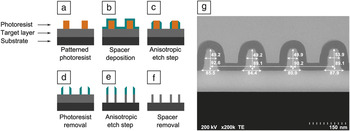
Plasma-enhanced ALD processes are becoming more popular, and several ALD equipment manufacturers have plasma-enhanced ALD reactors in their product portfolios. They can be used to synthesize films in devices that can benefit from the aforementioned merits. Examples include the deposition of low-resistivity metal nitride filmsReference Profijt, Potts, van de Sanden and Kessels9 employed as electrodes or the deposition of low-temperature oxides employed for encapsulation of polymeric or organic devices by O2 and H2O permeation barriers.Reference Langereis, Creatore, Heil, van de Sanden and Kessels14 Another application that illustrates the capabilities of plasma-enhanced ALD and has recently been introduced in manufacturing in the most advanced semiconductor technology nodes is wafer patterning. In “spacer-defined double patterning,”Reference Beynet, Wong, Miller, Locorotondo, Vangoidsenhoven, Yoon, Demand, Park, Vandeweyer, Sprey, Yoo and Maenhoudt15 ALD is used to deposit an oxide film, typically SiO2, on wafers with patterned photoresist (see Figure 2). The plasma process enables the use of low wafer temperatures compatible with the resist while also avoiding the need for long purge steps to remove H2O from the reactor and from the photoresist. The ALD process provides high conformality to cover the photoresist patterns fully and uniformly. After anisotropic etching of the SiO2 and stripping of the resulting exposed photoresist, a patterned SiO2 hard mask is created at half the original pitch. Moreover, the line width of the patterns is defined by the SiO2 film thickness. Spacer-defined double patterning therefore significantly extends the capabilities of existing lithography tool sets.
Spacer-defined double patterning process,Reference Beynet, Wong, Miller, Locorotondo, Vangoidsenhoven, Yoon, Demand, Park, Vandeweyer, Sprey, Yoo and Maenhoudt15 in which (a) a photoresist layer is deposited on top of the target layer and patterned using UV-exposure and photoresist development. In the next step, (b) a SiO2 spacer layer is deposited at a low temperature using plasma-enhanced atomic layer deposition, after which (c) an anisotropic etch is carried out. Subsequently, the photoresist is removed in step (d), after which (e) the pattern can be transferred into the target layer. Finally, in step (f), the SiO2 spacers are removed, after which narrow features at half-pitch are left. The scanning electron microscopy image in (g) shows the spacer material deposited on the patterned photoresist corresponding to step (b). The dimensions in this image are in nm.

Direct-write ALD
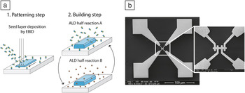
Due to its self-limiting surface reactions, ALD yields excellent growth control with submonolayer accuracy of the film thickness. ALD, however, yields no growth control of the film in the lateral dimensions such that top-down patterning techniques based on lithography are generally required to prepare nanostructures or nanopatterns comprising the ALD synthesized material. This has triggered the development of several area-selective ALD approaches, for example based on masking designated areas by photoresist films or self-assembled monolayers.Reference Biercuk, Monsma, Marcus, Becker and Gordon16, Reference Chen, Kim, McIntyre, Porter and Bent17 True bottom-up patterning can be achieved for several materials by a “direct-write ALD” method. This method exploits the fact that ALD processes are ruled by surface chemistry in which the nucleation on a substrate surface can be selective. Selectivity can be achieved for certain classes of ALD materials, such as platinum group metals, which often show a very long nucleation delay or no growth at all on certain substrates.Reference Aaltonen, Alén, Ritala and Leskelä18, Reference Knoops, Mackus, Donders, Notten, van de Sanden and Kessels19 Mackus et al. proposed a method in which Pt ALD films are deposited selectively on Pt seed layers, either prepared by plasma-enhanced ALD, or by electron- or ion-beam-induced deposition (EBID and IBID).Reference Mackus, Mulders, van de Sanden and Kessels20 With this method, which can be classified as energy-enhanced because plasmas or charged particle beams are involved, it is possible to confine the ALD reactions to the seed layer, which can be patterned on the nanoscale, for example, when focused electron or ion beams are employed during EBID or IBID. Figure 3a shows a schematic representation of an implementation of this direct-write ALD method for the synthesis of Pt nanopatterns. First, a very thin Pt seed layer is deposited using EBID, and subsequently the structure is built by ALD. During EBID and ALD, the same Pt-precursor ((MeCp)PtMe3; Me = methyl, Cp = cyclopentadienyl) can be used, and it has been shown that a seed layer of less than 1 nm is sufficiently thick to initiate the ALD growth. The O2 pulsing during ALD in the initial phase of the process also reduces the (very high) carbon impurity content of the EBID film, and Pt purity levels of virtually 100% were obtained for the nanostructures after ALD. The selectivity of the process has been demonstrated on several oxide surfaces and also on Pt seed layers prepared by a He-ion microscope.Reference Mackus, Mulders, Trompenaars, Dielissen, Weber and Kessels21 A similar process was also demonstrated for Pd. Compared to EBID and IBID processes, the main advantages of these direct-write ALD processes are the much higher chemical purity of the nanostructures and the significantly higher throughput of the method in cases when large footprints of nanopatterns need to be synthesized. Both aspects are illustrated by the example in Figure 3b in which a four-point structure with a large total footprint (>104 μm2) was fully synthesized by direct-write ALD. The resistivity of the direct-write ALD was found to be (11 ± 2) μΩ cm, close to the bulk value of Pt. This clearly shows that the merits of EBID or IBID in terms of patterning capability and resolution are combined with the merits of ALD (i.e., the high purity material and parallel processing of the surface). Moreover, the method has been implemented successfully in a scanning electron microscopy/focused ion beam system, although a system configuration with two separate chambers for seed layer deposition and ALD can also be advantageous.Reference Mackus, Mulders and Kessels22 Prototyping with direct-write ALD in the field of nanotechnology therefore seems within reach.
(a) Schematic representation of the direct-write atomic layer deposition (ALD) method combining electron- or ion-induced deposition (EBID or IBID) with ALD. The lateral dimensions of the structure are defined by the focused charged particle beam in the patterning step (step 1, electron or ion beam is represented by vertical arrows, precursor gas by colored species), creating a low-purity seed layer. During ALD (step 2, the ALD process is split up into two half reactions A and B), the structure is built layer-by-layer, leading to a high-purity material. Key to this approach is that the ALD growth occurs selectively on the seed layer material. (b) Scanning electron microscopy image of a four-point probe structure deposited by direct-write ALD on Al2O3. Similar structures can be applied for contacting nanoscale devices. The scale bar is 100 μm in the main image and 10 μm in the higher magnification image.

Inline atmospheric pressure ALD
Spatial ALD schemes allow for inline atmospheric pressure ALD processing. The precursor and reactant injection takes place in different compartments or zones in which the gas phase species are confined. The zones are separated by inert gas barriers created by purge zones in between. To have the substrate exposed alternately to the different zones, the substrate is moved through the zones. This movement can be linear by moving the substrate through many repeated zones, or it can be periodic by moving the substrates relative to the deposition head (see Figure 1d). SuntolaReference Suntola23 described the concept of spatially separated compartments for precursor and reactant dosing; however, Levy et al.Reference Levy, Freeman, Nelson, Cowdery-Corvan and Irving24, Reference Levy, Nelson and Freeman25 pioneered the spatial, open-air ALD configuration with a deposition head with gas barriers at atmospheric pressure. Levy et al. explored several designs of the technology in order to avoid mixing of the precursors and reactants, which was found to be one of the main challenges.Reference Levy, Nelson and Freeman25 With a carefully designed deposition head (employing linear inlet and exhaust slots for the gas and tailored pressure gradients) and with a configuration in which the substrates are basically left floating on the gas flowing from the deposition head (i.e., the gas flow supports the substrate), they arrived at a design that operated in pure ALD mode yielding very similar results to ALD in a closed reactor at reduced pressures. Having an ALD chemistry with fast reactions, however, is key in this technology, which was demonstrated for Al2O3 and ZnO, both employing precursors that are highly reactive with the H2O-exposed growth surface. With large-area electronics being the most promising application of spatial ALD, the feasibility of the technology was demonstrated by preparing ZnO-based thin-film transistors.Reference Levy, Nelson and Freeman25
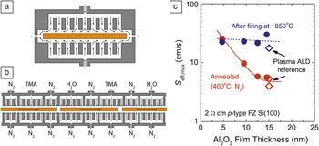
Another field of technology that requires the deposition of films over large surface areas is photovoltaics (PV). In this case, substrates, in the form of wafers, large glass sheets, or even flexible foils need to be covered by thin films at high throughput and at low cost. With (batch) ALD also being considered for several energy technologies,26–28 the inline atmospheric pressure ALD of Al2O3 was explored for surface passivation of crystalline silicon solar cells.Reference Granneman, Vermont, Kuznetsov, Coolen and Vanormelingen29–32 One system design is schematically illustrated in Figure 4. The “Levitrack” shown in this figure is a linear system in which the wafers (generally 156 × 156 mm2) are transported from one side to the other. With a special valve, the wafers are propelled at the track inlet, and subsequently they float on gas bearings with a constant velocity and with a self-regulating distance between the wafers due to pressure effects. During transport, they pass segments where their surfaces are sequentially exposed to Al(CH3)3, N2, H2O, and N2. The segments are repeated over the full track length, with the length of the track defining the final film thickness. Generally, the ALD precursors and reactants are injected from one side to achieve single-side deposition, although double-side deposition is also easy to implement (for batch ALD reactors, single-side deposition is challenging, as the surface texture and warping of the thin wafers hinders adequate back-to-back wafer stacking). Other advantages of this spatial ALD configuration are the absence of moving parts (apart from the wafers) and the fact that no deposition takes place at the reactor walls. Specific parts of the walls in a segment are exposed to only one precursor, purge, or reactant gas. Because ALD only occurs at the substrate surface and because the precursors and reactants are dosed in a continuous nature, the use of the (relatively expensive) precursors and reactants is also efficient. In its current configuration, the system yields ∼1 nm Al2O3 per 1 m system length. For an Al2O3 film of 10 nm thickness, this leads to a total system length of ∼10 m, which is a reasonable length for PV equipment. Moreover, the surface passivation achieved by a 10–15 nm thick Al2O3 film is excellent, as demonstrated by the low maximum surface recombination velocities achieved (see Figure 4c). It is comparable to the passivation obtained by state-of-the-art surface passivating Al2O3 films prepared by plasma-enhanced ALD.Reference Hoex, Heil, Langereis, van de Sanden and Kessels33, Reference Dingemans, van de Sanden and Kessels34 Furthermore, the passivation is sufficiently stable against the high-temperature “firing” step (∼850°C for a few seconds) used in commercial silicon solar cell production. After such a firing step, films with a thickness between 5 and 15 nm all show a similar level of passivation (see Figure 4c). Another spatial ALD approach is quite similar, although in this case, the wafers are moved back and forth under a deposition head.Reference Poodt, Lankhorst, Roozeboom, Spee, Maas and Vermeer31 Also for this approach, excellent surface passivation results were reported, demonstrating the robustness of the passivation properties provided by ALD Al2O3. Moreover, spatial ALD with a plasma-enhanced process has been claimed.Reference Poodt, Kniknie, Branca, Winands and Roozeboom35, Reference de Vries, van de Sanden, Creatore and Kessels36
The spatial atomic layer deposition (ALD) system “Levitrack” for inline processing of solar cell wafers (125 × 125 mm2 or 156 × 156 mm2, square or semi-square) at atmospheric pressure.Reference Granneman, Vermont, Kuznetsov, Coolen and Vanormelingen29 Cross-section of the system (a) perpendicular and (b) parallel to the direction of wafer flow, respectively. In (a), the injection of the gas (precursor, purge, or reactant) is shown making the wafers “float” on the gas at a self-stabilizing position in the middle of the track such that the wafers do not come in contact with the track walls. In (b), the segments are shown in which the wafer’s top surface is sequentially exposed to Al(CH3)3 (trimethylaluminum, TMA), N2, H2O, and N2. The distance between adjacent wafers of a few centimeters is self-regulating. (c) The maximum surface recombination velocity S eff,max for float-zone (FZ) Si(100) wafers passivated by Al2O3 thin films (filled circles) prepared in the Levitrack. Data are shown for different film thicknesses and before and after “firing” at ∼850°C. All wafers were annealed at 400°C in N2. Data for Al2O3 prepared by plasma ALD (open diamonds) are given as a reference.Reference Hoex, Heil, Langereis, van de Sanden and Kessels33, Reference Dingemans, van de Sanden and Kessels34 The figure shows that excellent passivation can be achieved by Al2O3 prepared by spatial ALD, even for ultrathin films and after an industrial “firing” process.

Roll-to-roll ALD
Roll-to-roll ALD of thin films is the ultimate goal for coating flexible substrates such as used in organic LEDs (OLEDs) and organic PV (OPV). Different inline concepts have been suggested to realize roll-to-roll ALD processes. Most of these are based on keeping the precursor gases in certain confined volumes and passing the substrate (or web) through these volumes to achieve the successive precursor doses required for ALD deposition. In this case, either only the substrate is moving, or both the substrate and gas volumes are moving. These studies are a first step to establish true industrial roll-to-roll ALD. First industrial pilot-scale roll-to-roll ALD systems are expected to be implemented within one to two years.
Currently, work on barrier process development with a true roll-to-roll ALD setup, where a flexible substrate passes through static precursor chambers (see Figure 1e), is in progress.Reference Dickey and Barrow37 This setup coats both sides and can run rapidly. Published results report up to 600 m/min. The results for Al2O3 and TiO2 are comparable to the ones reported for conventional ALD using gas pulsing. Due to the multiple substrate turns inside the coating system, this method is most suitable for the processing of polymer substrates due to their high flexibilty. Also, the possibility of using high line speed makes roll-to-roll ALD more compatible with applying barrier coatings to plastic substrates than with thin-film encapsulation of the actual devices ultimately prepared on the plastic substrates.
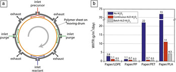
Recently, a commercial R&D tool for roll-to-roll ALD has been developed in which a continuous process takes place over a flexible substrate (dimensions 100 × 300 mm2) bent over a drum.Reference Maydannik, Kääriäinen and Cameron38 This drum, together with an outer cylindrical reaction chamber wall, forms a closed reaction chamber and provides the rotational movement to carry the substrate between the precursor zones. Spatial separation of precursors (similar to the case in Figure 1d) is achieved by having inert gas zones and exhaust lines between the precursor areas. One rotation of the drum results in one ALD cycle. The distance from the reactor wall to the substrate is approximately 1 mm. Maximum drum rotation is 1000 rpm, corresponding to a linear speed of 300 m/min.
Roll-to-roll ALD coatings have been applied to various polymers and polymerized papers for packaging purposes with the R&D system, shown in Figure 5a.Reference Lahtinen, Maydannik, Johansson, Kääriäinen, Cameron and Kuusipalo39 Al2O3 films were deposited with speeds ranging from 25 rpm to 500 rpm using 500 drum revolutions. The resulting film thickness of 50 nm corresponds to ∼1 Å/cycle growth rate, which is in-line with the growth-per-cycle obtained by ALD of Al2O3 carried out in the time domain. Significant improvement in terms of the reduction of the water vapor transmission rate of various extrusion coated paper materials was observed when coated with Al2O3 barriers (see Figure 5b). Such experiments demonstrate that roll-to-roll ALD can produce good water vapor and gas barriers and provide an important starting point for scaling up to industrial production tools. More efforts on Al2O3-based barrier films applied to different polymer substrates will likely be initiated, possibly combining Al2O3 with other thin-film materials in multilayer stacks. Roll-to-roll ALD might therefore become an enabling technology for flexible electronics when sufficiently good barrier properties are reached.
(a) R&D roll-to-roll atomic layer deposition (ALD) setup and (b) water vapor transmission rate (WVTR) results for polymer-coated papers having 100 nm thick Al2O3 films deposited on the polymer surface via a continuous (roll-to-roll) or batch ALD process. The figure demonstrates that the WVTR can be reduced by applying an Al2O3 film by roll-to-roll (continuous) ALD. Barrier films with low WVTR values are required for packaging applications. Measurement conditions are 23°C and 50% relative humidity.Reference Lahtinen, Maydannik, Johansson, Kääriäinen, Cameron and Kuusipalo39 LDPE, low density polyethylene; PP, polypropylene; PET, polyethylene terephthalate; PLA, polylactide.

Conclusion
The atomic layer deposition (ALD) method was developed over 35 years ago, but only recently has the semiconductor industry embraced ALD as one of its mainstream thin-film technologies. With its increased visibility and many of its merits demonstrated in device fabrication, the method is now being considered for application in a large number of emerging technologies, including several that require novel and even disruptive approaches with respect to process design, substrate material, and substrate delivery. The new reactor designs and ALD concepts discussed in this article clearly illustrate that the conceptually simple method of ALD lends itself very well to such novel innovative approaches. It is therefore expected that these and other future developments will significantly expand the capabilities of ALD in the next decade such that ALD-prepared films will also find wide-scale introduction in the technologies of the 21st century, including nanotechnology, photovoltaics, and organic electronics.