
I. INTRODUCTION
In past several years, organic–inorganic perovskite metal halides have been exhibiting unprecedented successes in several technological fields. With the hybrid metal halide film as the solar absorber, the photovoltaic efficiency increased from around 3% to above 22% in less than six years. Reference Zhang, Eperon and Snaith1 At the same time, halide perovskite thin film-based high efficiency light emitting diodes Reference Stranks and Snaith2 and photodetectors Reference Fang, Dong, Shao, Yuan and Huang3 have been demonstrated. Recently, optically pumped high quantum efficiency lasing Reference Zhu, Fu, Meng, Wu, Gong, Ding, Gustafsson, Trinh, Jin and Zhu4 has also been achieved in low-dimensional halide perovskite crystals. These immediate successes of metal halide perovskites have been partially attributed to their exhilarating electro-optic and optoelectronic properties. As direct band gap semiconductors, they carry very high absorption coefficients and simultaneously have extremely long electron/hole lifetimes and diffusion lengths. Reference Dong, Fang, Shao, Mulligan, Qiu, Cao and Huang5–Reference Chen, Wang, Shi, Hsu, Yang and Shi7 In the past several years, ferroelectricity Reference Liao, Zhang, Hu, Mao, Ye, Li, Huang and Xiong8,Reference Stroppa, Di Sante, Barone, Bokdam, Kresse, Franchini, Whangbo and Picozzi9 was discovered in several halide-based perovskites or perovskite structure-inspired compounds.
Along with the breakthroughs of metal halides in optoelectronics, recent studies have shown that metal halides could be promising materials in several other fields. Significant Rashba splitting Reference Crepaldi, Moreschini, Autes, Tournier-Colletta, Moser, Virk, Berger, Bugnon, Chang, Kern, Bostwick, Rotenberg, Yazyev and Grioni10–Reference Ishizaka, Bahramy, Murakawa, Sakano, Shimojima, Sonobe, Koizumi, Shin, Miyahara, Kimura, Miyamoto, Okuda, Namatame, Taniguchi, Arita, Nagaosa, Kobayashi, Murakami, Kumai, Kaneko, Onose and Tokura13 was recently proposed and revealed in several metal halide compounds, suggesting potential applications of these materials for novel spintronic logic and memory devices. More excitingly, recent explorations show that monolayer metal halide compounds may carry interesting ferromagnetic properties and even the quantum anomalous hall (QAH) effect. Reference Huang, Clark, Navarro-Moratalla, Klein, Cheng, Seyler, Zhong, Schmidgall, McGuire, Cobden, Yao, Xiao, Jarillo-Herrero and Xu14,Reference Huang, Zhou, Wu, Deng, Jena and Kan15
Fundamental studies have shown that the detailed crystal structure of the metal halides and also the related perovskite compounds play a critical role in enabling particularly interesting properties. With CsPbI3 as an example, despite the same stoichiometric ratio, its high-temperature perovskite phase carries much more demanded optoelectronic properties than that of its low-temperature yellow phase Reference Eperon, Paterno, Sutton, Zampetti, Haghighirad, Cacialli and Snaith16 for photovoltaic applications. In addition, the composition of metal halides may also significantly influence the ultimate physical properties. For example, holding the same perovskite crystal structure, the organic–inorganic metal halide perovskite has been revealed to have a longer photoexcited electron/hole lifetime than that of its inorganic counterpart. Reference Zhu, Miyata, Fu, Wang, Joshi, Niesner, Williams, Jin and Zhu17 Finally, it is shown that most of these recent breakthroughs in metal halide materials have occurred when they are produced at reduced dimensions: thin films, monolayers, and nanostructures (e.g., two dimensional nanoflakes, one-dimensional nanowires and zero-dimensional quantum dots).
All these progresses from both scientific understanding and technological breakthroughs pose stringent requirements on material synthesis. Growth controls on crystal structure, composition, and crystal morphology are mostly demanded. Metal halides compounds carry a wide range of crystal structures as shown in Fig. 1: CsCl structure, fluorite, layered, zinc blende, wurtzite, rocksalt, and perovskite. Many different binary metal halide compounds can form very populous intermediate phases of ternary/quaternary compounds. Two examples Reference Song, Watthage, Phillips, Tompkins, Ellingson and Heben18,Reference Kanno, Takeda, Masuyama, Yamamoto and Takahashi19 are given in Figs. 1(h) and 1(i). It is noted that when the crystal structures of two binary compounds are very different, the probability of forming intermediate phase compounds between them drastically reduces [Fig. 1(i)].
(a–g) Crystal structures of metal halides; (h, i) two examples of phase diagrams of metal halides. Reproduced with permission from Refs. Reference Song, Watthage, Phillips, Tompkins, Ellingson and Heben18 and Reference Kanno, Takeda, Masuyama, Yamamoto and Takahashi19.

The complexity in the crystal structures and compositions of metal halides and the requirement on their morphology control down to monolayer suggest that vapor phase epitaxy may be one of the most effective approaches for materials synthesis. In vapor phase epitaxy, two key growth parameters, temperature and pressure, can be controlled in a very sophisticated manner so that the film quality and morphology can be designed down to the atomic scale. The high-temperature processing is generally applied during the vapor phase epitaxy, which helps reduce the defects such as grain boundary and metastable phases in as-grown metal halide materials. Epitaxy can stabilize certain demanded crystal structures; a variety of vapor deposition growth methods, such as molecular beam epitaxy (MBE), sputtering, chemical vapor deposition (CVD), and physical vapor deposition (PVD) can be chosen to manipulate growth parameters to precisely control material compositions.
Motivated by these, in this review, we will cover two major aspects of metal halide materials: physical properties and vapor phase epitaxy. It is noted that there are many great review articles on the topic of optoelectronic/electro-optic properties of metal halide perovskites, but there is a vacuum on the comprehensive review of the interesting properties in general metal halide compounds. It is also noted that, it is the right time to assemble the most significant progresses on the vapor phase epitaxy of metal halides. Plenty of knowledge has been collected in the past several decades on this field. A timely review on this topic will help us better understand the growth kinetics and develop effective growth strategies especially for the recent metal halide perovskites and layered metal halides with promising applications in electro-optics, optoelectronics, and spintronics.
II. PHYSICAL PROPERTIES
Ionic bonds and van der Waals bonds are two typical bonding types found in most metal halide compounds. It has been found that the bonding energy of most ionic bonds in metal halides is relatively small. Correspondingly, many metal halides are very sensitive to external stimuli such as photon illumination, electron beam, radiation, chemicals, electric field, temperature, and pressure. The ultrasensitive character of metal halides to environmental perturbations, the extreme ionicity of their bonding nature, and the small bonding energy endow them with many interesting physical properties such as photodecomposition, electron beam-induced decomposition, low-density deep level defect states/high photon-electron conversion efficiency, chemically induced electrical conductivity modifications, ferroelectricity and so on. This section broadly summarizes the major physical properties in nonperovskite metal halides that people have discovered in the past several decades. We hope the review on these progresses in nonperovskite metal halides could help researchers gain a more fundamental understanding in researching perovskite metal halides and inspire new discoveries in more general metal halide compounds.
A. Photodecomposition
The relatively low decomposition temperature of metal halides makes them very vulnerable under photon irradiation. In 1893, Wells Reference Tubbs20 first observed PbBr2 turning to black upon exposure to sunlight. Two years later in 1895, Norris confirmed that black color was due to the formation of lead during irradiation and that bromine was lost during the process as well. In 1923, Sanyal et al. also reported bromine loss upon radiation. In 1964, 1965, Tubbs’s group Reference Tubbs20–Reference Dawood, Forty and Tubbs22 studied the photodecomposition of PbI2 in air or vacuum with the forms of single-crystal, polycrystalline, and evaporated film samples. Photolysis process led to the release of iodine and to the formation of lead. The decomposition rate followed the intrinsic absorption spectrum of PbI2, and the onset wave length was found to be at 530 nm. The photodecomposition of PbI2 was revealed not to occur at room temperature but increased exponentially with the temperature from 393 to 493 K. This was the first halide layer demonstrated to have high-resolution image recording applications. In 1966, Kaldor and Somorjai Reference Kaldor and Somorjai23 first studied PbCl2 using opaque layers with a thickness of 20 μm which were prepared by vacuum evaporation. Thermal decomposition of PbCl2 occurred above 473 K, and photodecomposition occurred above 298 K. Chlorine was released, leaving behind a dark gray lead precipitate after decomposition. The minimum photon energy required to initiate photodecomposition was found slightly lesser than that of the absorption edge. It was probably due to the electron transition from the valence band to the PbCl+ cation whose energy state is located at about 0.7 eV below the conduction band. In 1967, Spencer and Darlak Reference Spencer and Darlak24 studied microcrystalline PbBr2 dispersions which had a large surface-to-volume ratio. The dispersions of PbBr2 in polyvinyl alcohol–water solution were prepared at room temperature by simultaneously pipetting 25 mL Pb(NO3)2 and 25 mL KBr into 50 mL 0.5 wt% polyvinyl alcohol–water solution. Needle-like PbBr2 microcrystals were obtained which were several tens of microns long and shorter than one micron along radial directions. The photodecomposition rate was measured as the rate of lead production under an ultra-violet irradiation at 295 K. A linear relation between the lead production rate and intensity of irradiation was revealed.
In 1960, photodecomposition of CdI2 was observed by Fotland. Reference Fotland25 The sample was prepared by soaking filter papers into a concentrated CdI2 solution and then dried in air. Then the filter paper was exposed to a 100 W mercury arc lamp for 15 s. It was observed that the filter paper turned dark brown. The color change was due to the production of small cadmium particles near the surface upon photodecomposition. The sensitivity of CdI2 was determined by its intrinsic absorption spectrum. The sensitivity became significant with the wave length of light shorter than 410 nm. With its good resolution and high sensitivity, CdI2 print-out papers were widely used for recording ultra-violet light spots from galvanometer oscillographs and for preparation of light-sensitive electrophotographic materials. For instance, cadmium halides or lead halides were often added to silver halide–copper halides mixtures to further improve contrast or speed.
In addition to lead halides and cadmium halides, other halides with photodecomposition properties were also revealed: BiCl3, BiI3, SbI3, AgBr, and AgCl. Reference Tubbs26–Reference Sheppard and Vanselow33 The photolysis of these compounds was found to be useful in studying reaction kinetics and for imaging applications. However, the photolysis property should be carefully considered in characterizing the optoelectronic properties of these materials, especially at a low dimension. In addition, the fundamental understanding received in studying the photodecomposition of binary metal halides could be applied to investigate the photo-induced phenomena in metal halide perovskites.
B. Electron-induced decomposition
Besides photo-induced decomposition, as expected, people discovered that these metal halide compounds could be decomposed and evaporated under electron beams. In 1984, Muray et al. Reference Muray, Isaacson and Adesida34 used e-beam Ultra High Vacuum evaporation to prepare an 80 nm thick AlF3 amorphous film with high uniformity on thin carbon films and on 50-nm-thick Si3N4 windows. AlF3 can act as an e-beam resist, Reference Geis, Randall, Deutsch, DeGraff, Krohn and Stern35 which enables precise linewidth controllable lithography. AlF3 is a selfdeveloping resist, which volatilizes during exposure to radiation. To volatilize the AlF3 film to create patterns, the incident electron beam had an energy of 100 keV, a beam current of 10−11 A, and a spot size of 0.5 nm. Under such experimental conditions, it was found that a dose of 10 C/cm2 was sufficient to result in a total mass loss in the 80-nm-thick AlF3 film. Such a high-resolution resist enables replication of nanoscale patterns, down to several nanometers, onto Si3N4 and many other substrates. AlF3 film demonstrated a promising application as a resist for electron beam lithography, however, its requirement of an extremely high current density to vaporize the metal component limit is of practical use in device fabrication.
In 1992, Langheinrich et al., Reference Langheinrich, Spangenberg and Beneking36 used an electron gun evaporator to evaporate LiF and AlF3 powders in a weight ratio of 10:1 onto a liquid nitrogen-cooled substrate holder at about 90 K. The substrate was Si3N4 or thin carbon foil. Both the low-substrate temperature and a mixture of the two components with different structures prohibited the formation of crystals, resulting in a homogeneous and quasiamorphous AlF3-doped LiF film with high resolution and sensitivity. This LiF-based film can be effectively be evaporated under an electron beam energy of 100 keV and a beam current between 100 and 300 pA. The critical exposure was linearly related to the film thickness. The dose condition for this study was much less than that of the pure AlF3 case. Both the high resolution (below 7 nm) and high sensitivity of the AlF3-doped LiF film demonstrate a great capability of being a practical resist in device fabrication.
In addition to AlF3 and LiF, researchers Reference Kratschmer and Isaacson37,Reference Muray, Scheinfein and Isaacson38 also explored various metal fluorides as a positive and negative photoresist. A 50 nm thick FeF2 film was vacuum deposited and had a polycrystalline structure. When used as a positive resist, matrix dots of 4 nm in diameter were obtained under exposure conditions of 10 pC per dot exposure at 100 keV. Under high doses, a high amount of intrinsic stress was found to build up in parts of the film adjacent to positive exposures due to the loss of fluorine. When FeF2 was used as a negative resist, it was exposed at 20 keV and 250 nC/cm and then developed in water. Polycrystalline films of BaF2 and SrF2, typically 40 nm thick, were not suitable for positive resists, but their negative resists were developed. They were exposed to 20 keV electrons with a line dose of 100 nC/cm and then were developed in water since they were soluble in water. A 50 nm thick amorphous thin film of CrF2 resembles the structure and exposure properties of AlF3. When used as a positive resist at 20–50 μC/cm and 100 keV, clear patterns can be observed on the resist after selfdeveloping. However, the pattern cannot be transferred to a substrate because ion etching was inhibited by the leftover of a thin layer of Cr on the substrate after selfdevelopment. CsF formed islands, instead of continuous films on the substrate. It was used as a positive resist and exposed under 100 keV and 0.5 μC/cm. The line dose applied to CsF was very small because it had a very high sensitivity, almost two orders higher in magnitude than that of the AlF3 film of comparable thickness. Pattern characters of size 40 × 40 nm could be resolved.
C. Optoelectronic/electro-optic properties
Most metal halides are either semiconductors or insulators with a significant portion of them carrying band gaps at the UV regime. For a long time, people have been interested in exploring metal halides for optoelectronics and electro-optics. Though many heavy metal halide materials were used as radiation detection materials or as scintillating materials, wide interests in applying metal halides for much broader applications, such as solar cells, photodetectors, optically pumped lasing, and light emitting diodes have only emerged recently.
In 1961, Kuwabara and Aoyagi Reference Kuwabara and Aoyagi39 studied the photoconductivity of KI, KBr, and KCl in the fundamental absorption range between 203 and 383 K. A vacuum monochrometer was used to measure photocurrents of the crystal pressed between two electrodes. The light intensity during the experiment was kept constant at 1010 photons/cm2. Three characteristic regions were identified in their spectral: a bell-shaped peak in the low energy range due to impurities; a faint photoconductivity at the first absorption peak; and a photoconductivity arising from direct photoionization, which is temperature independent. Direct photoionization refers to that, free carriers are directly created by incident photons with energies larger than the ionization energy. The ionization in this spectra range occurs with almost a constant quantum efficiency independent of the photon energy or temperature.
Evans Reference Evans40 showed that SbI3 could be prepared by melting the mixture of pure antimony and iodine in a stoichiometric ratio in an evacuated silica tube. These crystals had their optical axis (c-axis) perpendicular to the crystal plate. Photoconductivity of SbI3 was conducted at room temperature on a Perspex aperture and was in contact with two spring-loaded platinum electrodes separated by 0.7 mm. In dark, the resistivity of SbI3 at room temperature was 109 Ohm cm. Photoconductivity was measured at various wave lengths of incident light while keeping the intensity, exposure time, and area constant. The potential difference between the electrodes was 20 V. The photocurrent reached two maxima at wavelengths of 580 and 440 nm. The current peak at 580 nm was due to an increasing rate of carrier recombinations as the absorption coefficient increases near the band gap, and the peak at 440 nm was contributed by a similar mechanism associated with exciton states of high energy.
Lefkowitz et al. Reference Lefkowitz, Lowndes and Yoffe41 applied a new technology to prepare thin single crystals of thallium halide. The TlBr crystals were obtained by thin sectioning a parent crystal with a modified ultramicrotome at room temperature while TlCl crystals were sectioned at about 373 K. The ability to obtain good single crystals enables further optical characterization of the materials. The absorption spectra of TlBr and TlCl were measured at 4 K. Two new exciton states for the (100) plane of TlBr were found at 401 and 399 nm. A band gap of 3.115 eV at Γ point was confirmed. The analysis on the absorption spectrum of TlCl showed two lines at n = 1 state, indicating a spin orbit splitting of the valence band. In 1967, Baldini and Bosacchi Reference Baldini and Bosacchi42 widely studied optical properties of alkali-halide crystals. They applied reflectivity measurements to single crystals of alkali halides in the ultraviolet region of the spectrum, in which excitonic and low interband transitions occurred. Based on both calculation results and their observation during experiments, they were able to predict properties of band structures of alkali halides, describe low-lying excited states, and establish a relation among energy levels of the conduction band, L bands, and the F center.
In 1977, Olive Less Hsu and Clayton Bates, Jr. Reference Hsu and Bates43 used a nonionizing light source to obtain excitation and emission spectra of well-annealed zone-refined CsI (Na) specimens in the temperature range from 300 to 4.2 K. Nonionizing light refers to the photon energy that is lower than the energy required to ionize atoms or molecules, that is, kicking off electrons above the vacuum level. Nonionizing light can have energy either higher or lower than the band gap energy. Two kinds of emissions were observed. One is the characteristic blue emission and others are low-temperature emissions. For the first time, they discovered that the characteristic emission consisted of two bands at 420 nm and 370 nm, respectively. Compared with calculated localized exciton energies, they concluded that the characteristic emission is due to the radioactive recombination of relaxed sodium impurity excitons. This study demonstrated the significance of excitation spectra in understanding the luminescence phenomenon of materials.
In 2002, Larruquert et al. Reference Larruquert, Méndez, Aznárez, Tremsin and Siegmund44 explored optical properties of evaporation-deposited thin films of CsI, KI, and KBr and their quantum efficiencies in the 53.6–174.4 nm spectral range. The optical constants were obtained from reflectance measurements. Effects of film heating and UV irradiation on the films’ optical properties and quantum efficiency were also investigated. The maximum absolute quantum efficiencies for as-deposited CsI, KI, and KBr were experimentally measured to be 0.85 at 105 nm, 0.78 at 52 nm, and 0.68 at 62 nm, respectively. It was found that KBr tended to have the highest stability upon thermal treatment and UV irradiation. KI film’s optical properties were clearly affected by UV exposure but were relatively intact upon heating. Both optical properties and the quantum efficiency of CsI were changed under conditions of heating or UV exposure. Correlations between the change in optical constants and the change in quantum efficiency were also determined.
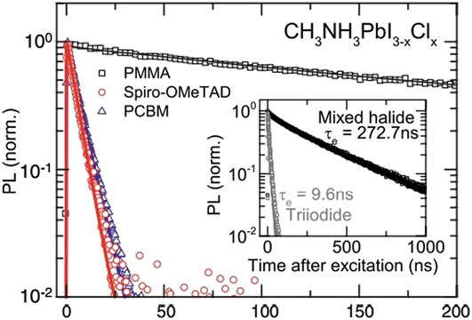
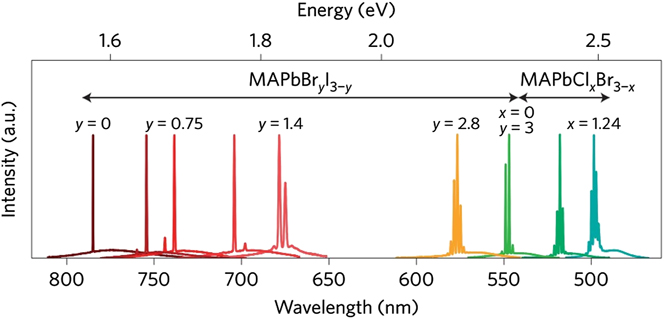
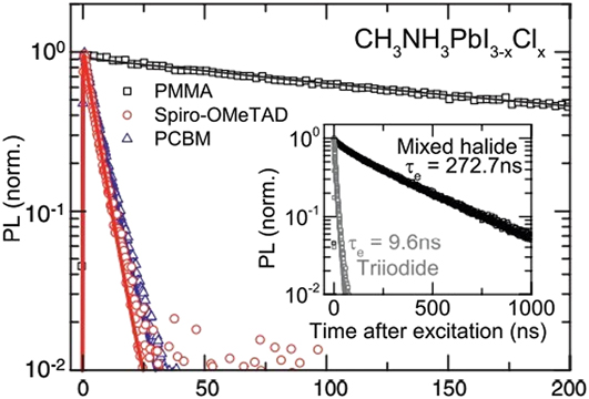
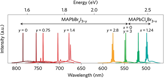
In addition to binary metal halides, Reference Campbell and Gao45–Reference Wood48 the study on the optoelectronic/electro-optic properties of the ternary metal halides was scarce before 1990. Very recently significant progress on understanding and revealing the optoelectronic/electro-optic properties of halide perovskites was made along with the technological breakthrough in their solar applications. One of the most significant discoveries Reference Stranks, Eperon, Grancini, Menelaou, Alcocer, Leijtens, Herz, Petrozza and Snaith6 was that a direct band gap semiconductor CH3NH3PbI3, at its thin film form, and the photoluminescence-based electron hole carrier lifetime could reach a few hundred nanoseconds and the electron/hole diffusion length exceeds one micrometer (Fig. 2). The high quantum efficiency of the ternary compounds led to a recent demonstration of optically pumped lasing Reference Zhu, Fu, Meng, Wu, Gong, Ding, Gustafsson, Trinh, Jin and Zhu4 (Fig. 3). Due to the focus of the current review, for more studies on the optoelectronic properties associated with metal halide perovskites, the readers are recommended to refer to related review articles such as. Reference Zhang, Eperon and Snaith1
Time-resolved PL of metal halide perovskite thin films. Reproduced with permission from Ref. Reference Stranks, Eperon, Grancini, Menelaou, Alcocer, Leijtens, Herz, Petrozza and Snaith6.
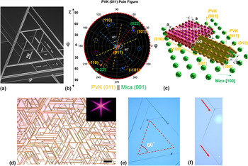
Lasing of metal halide perovskite nanowires. Reproduced with permission from Ref. Reference Zhu, Fu, Meng, Wu, Gong, Ding, Gustafsson, Trinh, Jin and Zhu4.
D. Magnetic properties
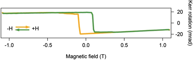
Serious studies on the magnetic properties of metal halides date back to several decades ago. In 1965, Dillon et al. Reference Dillon, Kamimura and Remeika49 studied magneto-optical properties of ferromagnetic chromium trihalides. The experimental investigations showed that the very large specific magnetic rotations were related to the absorption band edges of CrBr3 and CrCl3. Comparison with theoretical results enabled the attribution of the absorption band edge to the electron transfer transition between two orbitals. The large rotations which resulted from energy level splitting were due to spin–orbit interactions of the final state and the trigonal crystal field. In 2017, Xu et al. Reference Huang, Clark, Navarro-Moratalla, Klein, Cheng, Seyler, Zhong, Schmidgall, McGuire, Cobden, Yao, Xiao, Jarillo-Herrero and Xu14 demonstrated ferromagnetism in atomically-thin CrI3 flakes (Fig. 4). The CrI3 flakes were obtained by the mechanical exfoliation of bulk crystals and were then transferred to oxidized silicon substrates. The process was operated in a glove box under inert atmosphere. CrI3 flakes with a different number of layers were obtained with thickness of about 0.7 nm/layer. The layered structure enabled the study of thickness-dependent magnetism and the coupling between the underlying substrate and thin film if the interaction strength is strong. Magneto-optic Kerr effect measurements as a function of the applied external magnetic field were applied to probe the magnetic order of CrI3. The observed hysteresis loop and remnant magnetism at the zero external magnetic field confirmed the ferromagnetic ordering of CrI3 layers. Ferromagnetism of CrI3 varied with layer thickness, which was confirmed by their different hysteresis loops and remnant/saturation Kerr rotation values. The intrinsic ferromagnetism in monolayer CrI3 and its layer-dependent magnetic response revealed promising applications in investigating the emerging quantum effect in hybrid structures and in developing novel magneto-optoelectronic devices.
Magnetic properties of monolayer CrI3. Reproduced with permission from Ref. Reference Huang, Clark, Navarro-Moratalla, Klein, Cheng, Seyler, Zhong, Schmidgall, McGuire, Cobden, Yao, Xiao, Jarillo-Herrero and Xu14.

Kyungsoo Ahn et al. Reference Ahn, Kremer and Simon50 used powder neutron diffraction on the triangular-layer system Tb2C2I2 to investigate the effects of geometrical frustration on its magnetic properties. Below 60 K, strong resolution-limited magnetic Bragg reflections were observed due to commensurate antiferromagnetic long range (afm) ordering. Above this, the commensurate afm transition at 60 K and the magnetic behavior of Tb2C2I2 can be divided into three regions. Below 150 K, increased afm short-range correlations developed within the Tb atom double layers. Interplane correlations kicked in when the temperature was below 95 K. The interplane correlations remained short ranged at about 1 nm. Sizable interplane correlations started to develop when the temperature was reduced close to 87 K. These sizable interplane correlations were raised from extended intraplane correlations, which grew rapidly in a sharp temperature range around 87 K. The discontinuous transition of interplane correlations growth resulted in the transition from the commensurate phase to the incommensurate phase due to the magnetic fluctuation of Tb moments as the temperature increased above 87 K.
Kasten et al. Reference Kasten, Moller and Schienle51 explored the magnetic ordering in GdI2. The GdI2 powder samples were prepared from a solid state reaction between GdI3 and metallic Gd. The powder samples were composed of tiny platelet-shaped crystals in a hexagonal structure with the c-axis perpendicular to the plane. The GdI2 crystal possessed a strongly two-dimensional structure with Gd layers separated by two I layers along the hexagonal c-axis. AC susceptibility measurements were performed on the sample with changing temperature. It was observed that under about 290 K, GdI2 had a very high temperature-independent susceptibility under a zero external magnetic field. As temperature increased higher than 290 K, there was a sharp decrease of susceptibility at around 295 K due to metallic Gd impurities. Above the material’s Curie temperature, T C = 313 K, the susceptibility remained almost constant up to 400 K, so no Curie–Weiss behavior was observed in this temperature range. Effects of small external magnetic fields (<0.03 T) on susceptibility were also investigated. It was found that above T C, the external magnetic fields had no influence on the susceptibility while below T C, the susceptibility dropped dramatically upon the application of a static magnetic field and was reduced to the susceptibility value above T C within a few mT and stayed constant with the further increased magnetic field. The analysis of the crystal structure and ground spin state of ions revealed a two-dimensional magnetic interaction with superexchange via conduction band electrons within one layer. The large-high temperature susceptibility compared to metallic Gd indicated that the dominant magnetic ordering is a ferromagnetic interaction. Besides, the absence of the Curie–Weiss behavior can be explained by two-dimensionality of the Heisenberg interaction. On the other hand, the low-temperature experiments confirmed the antiferromagnetic intersublattice coupling. This ideal Heisenberg, two-dimensional system is very appealing for both experimental and theoretical studies.
Recently, Huang et al. Reference Huang, Zhou, Wu, Deng, Jena and Kan15 used first principle calculations to theoretically predict the QAH effect in the ferromagnetic transition metal halide RuI3 monolayer. The RuI3 monolayer was predicted to be an intrinsic ferromagnetic QAH insulator with a topologically nontrivial band gap of 11 meV at the Fermi level attributed to its crystal symmetry. As a consequence, the QAH effect of RuI3 was expected to be robust. Strain engineering was also proposed by the authors to be a possible method to manipulate the crystal’s exchange energy and band gap. The robust QAH effect in RuI3 showed promising applications in nanoelectronics and spintronics. These recent experimental and theoretical progresses in exploring the magnetic properties of low-dimensional metal halides may inspire exciting discoveries in halide systems. Reference Felser, Ahn, Kremer, Seshadri and Simon11,Reference Joseph and Schlömann52,Reference Zhou, Lu, Zu and Gao53
E. Chemical-induced electrical conductivity modification
The ionic nature of metal halides makes these materials sensitive to certain gases. In 1999, Lauque et al. invested the sensor characteristics for the NH3 gas of CuBr films. Reference Lauque, Bendahan, Seguin, Pasquinelli and Knauth54 The CuBr film was prepared by Radio Frequency Sputtering (RF sputtering) on the epoxy substrate. The RF power used in the experiment was 50 W, the targets are CuBr targets formed by pure CuBr powder, and the sputtering was conducted under an argon pressure of 3 Pa. The substrate was kept at room temperature during sputtering. The as-deposited film showed a randomly orientated polycrystalline γ-CuBr structure confirmed by X-ray diffraction. To investigate the film’s electrical conductivity in the presence of ammonia gas, the film on the epoxy substrate was then combined with interdigital copper electrodes. It was shown that the DC conductivity of CuBr film reduced upon increasing partial pressure of NH3. The electrical response was also very fast, in the order of a few seconds. The reduction in DC conductivity was believed to be caused by strong interactions at the gas–solid interface between CuBr and NH3. This interaction resulted in formation of surface copper ions and these positive surface charges were balanced by an adjacent space charge region enriched in copper vacancies and electrons. The increased electron concentration decreased the original p-type conductivity of the film. Besides, the adsorbed NH3 gas on the film surface increased the interfacial resistance and further reduced its DC conductivity. The sputtered CuBr film demonstrated a promising application as a faster response sensor for NH3. In 2004, the same group, Lauque Reference Lauque, Bendahan, Seguin, Ngo and Knauth55 developed high sensitivity and selective room temperature NH3 gas microsensors based on a CuBr film. In the presence of ammonia, the reaction between ammonia molecules and copper ions on the film surface result in a large decrease in the film conductivity, which can be used as a sensing signal. The operation ammonia concentration is between 1 and 500 ppm. Its high sensitivity, selectivity, and ability to operate at room temperature provides itself with great practical application possibilities.
Besides CuBr, a similar sensing behavior occurs in AgCl. In 1990, Lauer, Maier, and Gopel Reference Lauer, Maier and Gopel56 investigated conductance effects of ammonia on different types of AgCl films. The three kinds of films were epitaxial: AgCl film on the (100) NaCl substrate, polycrystalline AgCl film on sapphire, and freestanding AgCl film. The epitaxial (100) AgCl films were prepared by evaporating pure AgCl onto NaCl single crystals with thickness of 150, 200, and 300 nm. The polycrystalline films with thickness of 100 nm were obtained also by evaporation onto a sapphire substrate. Annealing was necessary for both films in contact with a substrate to achieve equilibrium conductivity. The freestanding films with thickness of 190–200 nm were prepared by the precipitation of AgCl from AgNO3 and HCl under protective light. The film conductivity measurements were carried out with an impedance bridge in the temperature range of 373–443 K and an ammonia partial pressure range of 103–105 Pa. The conductivity of the AgCl film was determined by two competing factors. First, the AgCl is p-doped by Ag+ vacancies. So, an increased concentration of Ag+ vacancies enhances the film’s conductivity. Thus, with the presence of ionophilic NH3 gas, the Ag+ cations combined with the NH3 molecule to form complexes that increased Ag+ vacancies, which resulted in an increase of conductivity. Second, the adsorption layer of gas such as NH3 results in interfacial transfer resistivity, reducing the film conductivity. Thus, upon the presence of NH3 gas, the conductivity of the AgCl film decreased and the response time was usually 1–5 min in the temperature range of 373–973 K, revealing a possible application in the gas sensing field. In addition to NH3, several other gases such as CO2 sensing Reference Rao, Bleek, Schoonman and Sorensen57–Reference Maier65 were also practiced.
F. Ionic conductivity
The low decomposition temperature of metal halides suggests that the defect formation energies in these materials are relatively small compared to those of oxides dielectrics. Both low decomposition/melting temperatures and low-defect formation energies may make these materials interesting for battery-based applications concerning ionic conductivity. In 1986, Coetzer Reference Coetzer66 reported the first disclosure of a high energy density system that used transition metal chlorides as a solid cathode. Solid electrolyte β-alumina was used as a separator. The second electrolyte, molten NaAlCl4, was incorporated with the cathode, and the electrochemically active species in cathode was insoluble in this molten salt electrolyte. This second liquid electrolyte served to transport sodium ions between β-alumina and the reaction zone in the cathode. This battery set-up had low cost and high safety reliability, possessing great potential for a wide range of commercial applications, such as vehicle traction, load leveling, and aerospace applications.
Another example is associated with sodium/nickel chloride battery. In 2001, Sudworth Reference Benato, Cosciani, Crugnola, Sessa, Lodi, Parmeggiani and Todeschini67 explored the operating principle, performance, production and applications of sodium/nickel chloride battery. The sodium/nickel chloride cell is composed of molten sodium as the negative electrode, nickel or nickel chloride as the positive electrode during discharging or charging processes, respectively, and molten sodium tetrachloroaluminate (liquid) and β-alumina (solid) as the electrolyte. The liquid component of the electrolyte promoted the rapid transport of sodium ions between the nickel chloride electrode and the solid ceramic electrolyte. The minimum operating temperature of the cell is determined by the melting temperature of its electrolyte, 430 K, but the optimal temperature range for the best battery performance was found to be between 543 and 623 K. The performance of cells was found to be optimal under a current limit of 15 A per cell for a 32 A h cell and with a charging voltage of 2.67 V. The sodium/nickel chloride battery could be used in both pure electric and hybrid vehicles, telecommunications, and marine applications. In addition, there are several other examples that take advantage of the ionic character of metal halide films for battery applications. Reference Li, Lu, Kim, Lemmon and Sprenkle68–Reference Galloway and Haslam86
G. Radiation-induced electrical conductivity modification
The semiconducting nature and the involvement of heavy elements of metal halides make them ideal for radiation detection. In 1948, Hofstadter Reference Hofstardter87,Reference Milbrath, Peurrung, Bliss and Weber88 reported the discovery of scintillator NaI mixed with a small amount of thallium. The sample was prepared in vacuum in a 0.5-inch quartz tube. Its radiation detection capability was tested by exposure to a source of 0.1 mCi radium at 16 cm at room temperature. The response of the sample was characterized by light flashes emitting in about one microsecond or less, indicating a quick response as a detection material. This discovery revolutionized the field of radiation detectors.
In 1970, Roth and Willig Reference Roth and Willig89 studied PbI2 as nuclear particle detectors. The PbI2 detector was made from platelets of vapor-grown single crystals with 1 cm diameter. The front contact of the gold layer was deposited by evaporation and was connected to a copper wire by a silver paste. The rear contact used a silver paste film. The pulse height was measured, which is proportional to the number of collected charge carriers created from particle radiation. Both α and γ particles were counted in the temperature range from 73 to 403 K. The operation temperature range of PbI2 was larger than that of other semiconductor detectors such as CdTe, Si, and Ge. It also had better γ-ray absorption properties. The reports demonstrated a promising application of PbI2 as an accurate radiation detector with a wider operation temperature range.
van Loef et al. Reference Milbrath, Peurrung, Bliss and Weber88,Reference van Loef, Dorenbos, van Eijk, Krämer and Güdel90 used optical, X-ray, and γ-ray excitations to study scintillation properties of LaCl3 doped with different concentrations of Ce3+. It was found that the activator, Ce3+ ion had emission peaks at 330 and 352 nm under optical and γ-ray excitation. The samples with Ce3+ concentration varying from 2% to 30 and 100% had photon yields of 46,000 ± 3000 photons per MeV of absorbed γ-ray energy. It was also found that the short decay component of the total light yield in the scintillation decay curve increased with the Ce3+ concentration. The energy resolution was measured and the highest resolution of about 3.1% was given by the sample with 10% Ce3+. Ce3+ activated LaCl3 had been demonstrated to be faster and more efficient for high-energy resolution scintillation.
LaBr3 was studied as a scintillating material intensively. Reference Milbrath, Peurrung, Bliss and Weber88,Reference Shah, Glodo, Klugerman, Higgins, Gupta and Wong91,Reference van Loef, Dorenbos, van Eijk, Krämer and Güdel92 Recently, Shah et al. studied the Ce3+ doped LaBr3 scintillator for γ-ray spectroscopy. The crystals were prepared using the Bridgeman method. The molar concentration of Ce3+ in LaBr3 crystals was 0.5%. Under gamma ray excitation, the Ce3+ emission peaked at 360 nm. The sample had a large light output larger than 60,000 photons/MeV and a fast principle decay constant smaller than 30 ns. The energy resolution was about 2.6% for the 662 keV full absorption peak. A study conducted by van Loef et al. on 0.5% Ce3+ doped LaBr3 showed similar properties under γ-ray excitation. These research results confirmed that LaBr3–Ce could be one of the ultimate choices for a scintillator, especially in the case where good energy resolution and fast luminescence decay are required.
Heavy metal halide LuI3 was also explored for radiation detection. Reference Milbrath, Peurrung, Bliss and Weber88,Reference Birowosuto, Dorenbos, van Eijk, Krämer and Güdel93 In 2006, Birowosuto et al. investigated the scintillation properties of Ce3+ activated LuI3. Single crystals of Ce3+ doped LuI3 were prepared by the Bridgmann technique. γ-ray pulse height spectra of samples were recorded. An extremely high light output of 92,000 e–h+ pairs/MeV was observed for LuI3: 5% Ce3+. The best energy resolution of 3.3% at 278 K was obtained in the sample with 0.5% Ce3+ and a light output of 50,000 e−–h+ pairs/MeV. The γ-scintillation decay spectra presented that about 50% of the total light yield was produced within 50 nm. Its very high light output, acceptable energy resolution, and reasonable high density made itself a material of interest in this field.
H. Superconductivity
Encouraged by the great success of high-temperature oxide superconductors with layered structures, different layered metal halide materials Reference Chen, Koiwasaki and Yamanaka94–Reference Yamanaka and Tou98 have been proposed and studied in the search of high T C superconductors. In 1996, Henn et al. Reference Henn, Schnelle, Kremer and Simon99 applied resistivity, susceptibility, and specific heat measurements to characterize the superconducting state of layered superconductors Y2C2I2 and Y2C2Br2. Single phase samples of Y2C2X2 (X = Br, I) were prepared by heating a mixture of Y metal chips, YX3, and graphite powders in sealed tantalum crucibles at 1320 Both electrical resistance measurements from 300 to 4 K and susceptibility measurements in an external field of 1 mT from 2 to 15 K were conducted. The sudden vanishing of electrical resistivities were observed at 5.0 and 10.0 K for Y2C2Br2 and Y2C2I2, respectively. Besides, the dramatic decrease of magnetic susceptibilities occurred at 5.04 and 9.97 K for Y2C2Br2 and Y2C2I2, respectively. These results from two measurements agreed well with each other, so the superconductivity temperature was confirmed to be 9.97 K for Y2C2I2 and 5.04 K for Y2C2Br2. The heat capacities obtained from the two compounds were in excellent consistence with the two-fluid model, indicating a moderately strong electron-phonon coupling which increased the transition temperature.
In 1996, Shoji Yamanaka et al. Reference Yamanaka, Kawaji, Hotehama and Ohashi100 discovered a new layer-structure nitride, β-ZrNCl displaying superconducting property upon intercalation with lithium. The β-ZrNCl crysral is formed by sandwiching ZrN double layers between two close packed chloride layers, represented as [Cl–Zr–N]–[N–Zr–Cl]. It was confirmed by XRD that the crystal possessed a rhombohedral unit cell with three layers. The β-ZrNCl crystals were prepared by reaction of ZrH2 and NH4Cl at 650 °C. The lithium intercalation was conducted by dispersing β-ZrNCl into 15% n-butyllithium (Bu-Li) solution. The final product obtained had the formula of Li x ZrNCl with x = 0.16. Both magnetic susceptibility under field intensity of 50 Oe and electrical resistivity of Li x ZrNCl were measured with changing temperature. These two measurements reveal a superconducting transition temperature of 12.5 K. Besides the observed hysteresis loop, magnetization measurement indicated that the lithium intercalated β-ZrNCl is a type-II superconductor. Later in 1998, Yamanaka et al. showed this material exhibited a superconducting state with a high Curie temperature of 25.5 K with processing optimization. Reference Yamanaka, Hotehama and Kawaji101
Very recently, Yin and Kotliar Reference Yin and Kotliar102 proposed a design guideline to prepare mixed-valent high-T C superconductors. They used first-principles calculations and focused on increasing Curie temperature of thallium halide-based compounds, in which superconducting state arises due to a strong electron-phonon coupling. Superconducting properties of CsTlF3 and CsTlCl3 were studied with various hole doping levels and volumes and the Curie temperatures were predicted to be 30 and 20 K with ∼0.35/f.u. hole doping at modest pressures, ∼10 and ∼2 GPa, respectively.
I. Rashba splitting
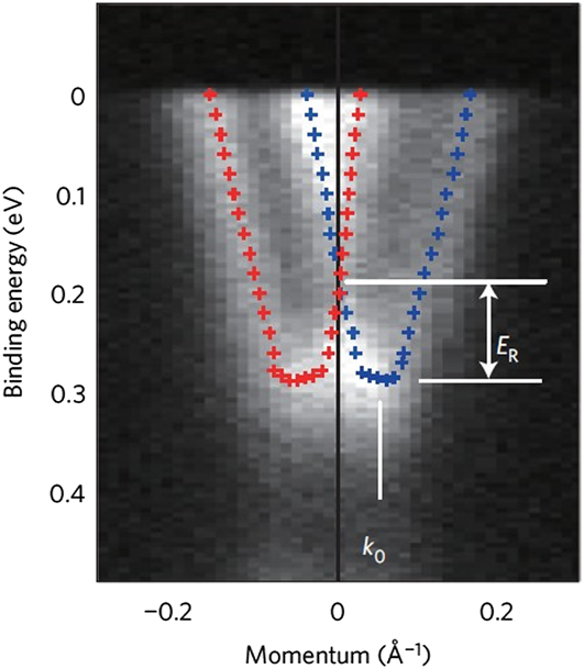
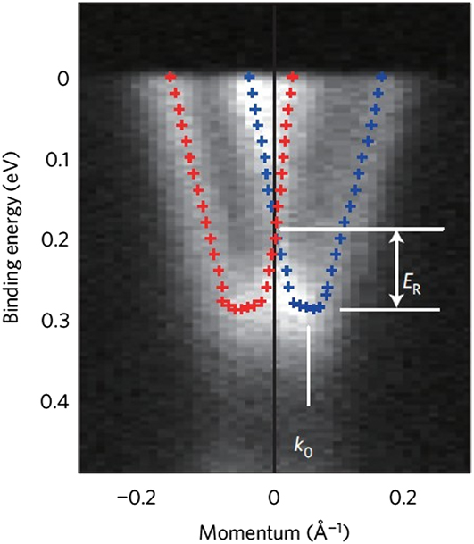
Rashba splitting as a consequence of strong spin-orbital interactions and a lack of inversion symmetry, suggesting promising applications in the field of logic computation and memory (e.g., spintronics), has been discovered in several halide materials. Reference Crepaldi, Moreschini, Autes, Tournier-Colletta, Moser, Virk, Berger, Bugnon, Chang, Kern, Bostwick, Rotenberg, Yazyev and Grioni10,Reference Eremeeva, Nechaev and Chulkov12,Reference Maass, Bentmann, Seibel, Tusche, Eremeev, Peixoto, Tereshchenko, Kokh, Chulkov, Kirschner and Reinert103–Reference Butler, Yang, Sankar, Lien, Lu, Chang, Chen, Wei, Chou and Lin109 In 2011, Ishizaka et al. Reference Ishizaka, Bahramy, Murakawa, Sakano, Shimojima, Sonobe, Koizumi, Shin, Miyahara, Kimura, Miyamoto, Okuda, Namatame, Taniguchi, Arita, Nagaosa, Kobayashi, Murakami, Kumai, Kaneko, Onose and Tokura13 discovered a giant Rashba-type spin splitting in bulk BiTeI (Fig. 5). The single crystals of BiTeI were prepared by the Bridgeman method. It was confirmed that there existed a huge spin–orbit interaction in the polar semiconductor BiTeI, which contains heavy elements. Due to this strong spin–orbit interaction, bulk carriers were ruled by the Rashba effect, which lifted the electron-spin degeneracy, resulting in spin splitting. The observed band splitting and spin polarization were consistent with first-principles calculation. In 2013, Landolt et al. Reference Landolt, Eremeev, Tereshchenko, Muff, Slomski, Kokh, Kobayashi, Schmitt, Strocov, Osterwalder, Chulkov and Dil110 applied angle-resolved photoemission spectroscopy (ARPES) in the ultra-violet and soft X-ray regime to explore the giant Rashba spin splitting in the bulk conduction and valence bands of BiTeCl. ARPES enabled separation of bulk and surface contribution of the electronic structure and revealed that the Te-terminated (0001) crystal surface had spin-split two-dimensional surface states. A large Rashba splitting of both the bulk and surface states of BiTeCl was observed. Together with its large band gap and macroscopic crystallinity, it became an interesting material for spin transport measurements. Reference Chen, Kanou, Liu, Zhang, Sobota, Leuenberger, Mo, Zhou, Yang, Kirchmann, Lu, Moore, Hussain, Shen, Qi and Sasagawa111 In 2013, Eremeev et al. Reference Eremeev, Rusinov, Nechaev and Chulkov112 using the density functional theory studied the bulk and surface states of BiTeBr. It was found that the ordered BiTeBr is more energetically preferable than the disordered phases according to relativistic ab initio calculations. Both Te-terminated and Br-terminated BiTeBr showed surface states with giant spin–orbit spin splitting due to potential bending within the near-surface layers. The Te-terminated surface states could be identified as Rashba-split states with a coupling parameter of 2 eV Å. These states had larger a Rashba splitting and a wider band gap than those of BiTeCl and larger splitting off from the bulk conduction band and more isotropic energy dispersion within the band gap compared with BiTeI.
Rasha splitting in BiTeI. Reproduced with permission from Ref. Reference Eremeeva, Nechaev and Chulkov12.
Recently, it was shown that the perovskite halide may also carry Rashba splitting. In 2014, Kim et al. Reference Kim, Im, Freeman, Ihm and Jin113 theoretically proposed an organic–inorganic hybrid metal halide perovskite AMX3 (A = CH3NH3, M = Pb and Sn, X = I and Br) as a promising ferroelectric Rashba material. It was shown that the ferroelectric switching which resulted from changing external electric fields could be used to control the helical direction of the angular momentum texture in the Rashba band. Theoretical calculations confirmed the direct coupling between S = 1/2 and J = 1/2 Rashba bands and ferroelectric polarization at valence and conduction band edges. In these hybrid halides, ferroelectric polarizations generated two distinct Rashba bands with different spin and orbital angular momentums. Meanwhile, Alessandro Stroppa et al. Reference Stroppa, Di Sante, Barone, Bokdam, Kresse, Franchini, Whangbo and Picozzi9 used density function theory simulations and symmetry analysis to investigate a new low-energy structure for lead-free perovskite iodide FASnCl3 with a planar formamidimium cation FA = (NH2CHNH2)+. It was shown that this material possessed a highly tunable ferroelectricity which was of interest for multistate logic and strong spin–orbit coupling which gave rise to the coexistance of Rashba and Dresselhaus effects. At low temperatures, the ferroelectric polarization can be induced and tuned in both magnitude and direction. The coexistence of Rashba and Dresselhaus effects in FASnI3 may be manipulated by an electric field that changes the ferroelectric state, giving rise to unique optical and electronic properties and new features for novel optoelectronic and spintronic devices.
J. Ferroelectricity
The existence of ferroelectricity in metal halides was initially revealed in SbSI crystals. In 1962, Fatuzzo et al. Reference Fatuzzo, Harbeke, Merz, Nitsche, Roetschi and Ruppet114 studied the ferroelectric properties of SbSI crystals. In the form of an orthorhombic structure, the single crystal of this V–VI–VII compound had the shape of a thin needle with the c-axis being the needle axis. Dielectric constant measurements were performed to investigate the samples’ ferroelectric properties. It was found that SbSI had a Curie temperature of 295 K and a high spontaneous polarization of 25 μC/cm2 with a small coercive field strength of 100 V/cm at 273 K. The ferroelectric axis was the needle axis (c-axis). As the temperature increased, the polarization decreased and suddenly dropped to zero at the Curie point, indicating a first order transition.
Recently, significant interests have been emerging in the perovskite or perovskite-inspired halides. Reference Zhang, Pan, Yang, Wang, Su, Yang, Huang, Han and Poeppelmeier115–Reference Liu, Zheng, Koocher, Takenaka, Wang and Rappe126 In 2014, Pilania and Lookman Reference Pilania and Lookman127 used first-principles based density-functional theory computations to investigate the geometry and electronic structure of RbHgF3. It was shown that RbHgF3 with Pnma space group can accommodate epitaxial compressive and tensile strains by tilting and rotation of HgF2 octahedrals. These octahedral rotations resulted in Rb-site antipolar displacements, thus creating an A-site cation ordering in fluoroperovskite superlattices along [001] direction. The coupling between octahedral rotations and cation antipolar modes gave rise to net polarizations of 4.39 μC/cm2 and 1.70 μC/cm2 in RbHgF3/NaHgF3 and RbHgF3/KHgF3 superlattices, respectively. In 2015, Pilania and Uberuaga Reference Pilania and Uberuaga128 studied the electronic structure, energies of cation ordering, and the biaxial strain effect on a newly designed double perovskite CsRbCaZnCl6 by first-principles calculations based on density functional theory. Two ABX3 constituents were chosen to form the double perovskite: CsCaCl3, which was thermodynamically stable with a cubic perovskite structure but was not not strain sensitive and RbZnCl3, which was unstable in the perovskite phase but ultra-sensitive to the epitaxial strain in this phase. When combined together, these two compounds interacted synergistically and resulted in a stable perovskite phase with a high strain response. The calculations predicted a layer-ordering for the A-site cation and a rock salt-type ordering for the B-site cation. It was shown that the electronic structure and band gap were mainly affected by the B-site instead of the A-site cation ordering. The theoretical calculations proposed a possible a phase transition from a paraelectric ground state to an antiferroelectric state that can be realized by an experimentally achievable compressive epitaxial strain of about 2.5%. Since the energy barrier of transition from the antiferroelectric state to the ferroelectric state was estimated to be only about 24 meV/f.u. for 3% compressive strain, it was possible for the material to switch to the metastable ferroelectric state.
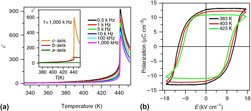
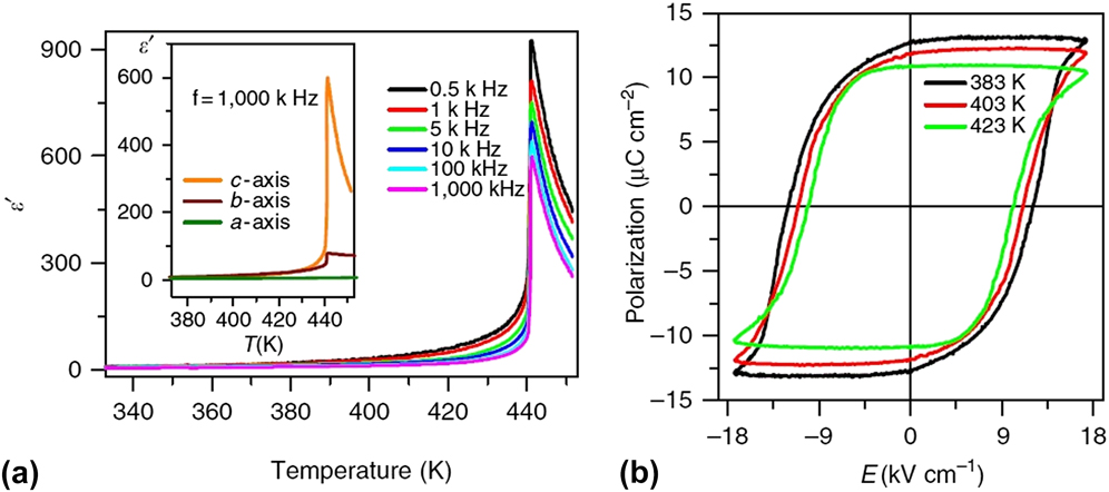
In 2015, Liao et al. Reference Liao, Zhang, Hu, Mao, Ye, Li, Huang and Xiong8 investigated layered perovskite (benzylammonium)2PbCl4 and showed that it was ferroelectric with semiconducting behaviors (Fig. 6). Small crystals of the sample were obtained by mixing PbCl2 and benzylammonium chloride stoichiometrically in concentrated HCl solution. Larger crystals were produced by a slowly evaporating N,N-dimethylformamide solution at 363 K. The ferroelectric property of the sample was measured by the polarization electric field (P-E) hysteresis loop above 383 K. It was shown that the sample had a saturated polarization of about 13 μC/cm2 with a relatively high coercive field, and its remnant polarization was almost equal to the saturated one. The Curie temperature was 438 K and a band gap of 3.65 eV was measured by optical ultraviolet-visible absorption spectrum. The experimental results demonstrated the material to possess high-temperature molecular ferroelectric properties and semiconducting behaviors. High-mobility ferroelectric semiconducting is always a demanded material property for developing high-performance photo-ferroelectric memory/photovoltaic devices.
Ferroelectricity in layered perovskite (benzylammonium)2PbCl4. Reproduced with permission from Ref. Reference Liao, Zhang, Hu, Mao, Ye, Li, Huang and Xiong8.
III. VAPOR PHASE EPITAXY
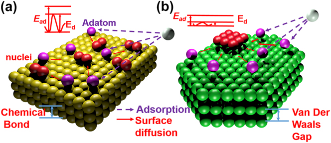
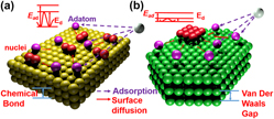
The exploration of these interesting properties of metal halides and their applications at the device/circuit level demand high quality materials, mostly at a reduced dimension such as a nanowire, a monolayer, and a thin film. Vapor phase epitaxy, already proved in the semiconductor industry, can produce materials with the desired morphology and crystal quality. This section thus reviews the knowledge collected in the past on growing metal halides via vapor phase epitaxy, which is categorized by the crystal structures of grown materials and the types of epitaxial substrates. Table I summaries the major parameters in vapor phase epitaxy and in growth results. Among all these growth approaches, two major mechanisms have been extensively explored: chemical epitaxy and van der Waals epitaxy (Fig. 7). In chemical epitaxy, the interactions between grown materials and substrates are strong chemical bonds, while in van der Waals epitaxy, they are weaker van der Waals interactions. To realize van der Waals epitaxy, the grown materials or substrates should be 2D materials to get rid of dangling chemical bonds. Reference Utama, de la Mata, Magen, Arbiol and Xiong129 In the vapor phase epitaxy of metal halides, substrates have been shown crucial. In this review, the substrates are classified into three main categories: halide insulator, semiconductor, and metal. Epitaxy can be achieved with a large lattice mismatch when growing metal halides on metals or on halide insulators. However, when growing metal halides on semiconductors such as III–V compounds, the epitaxy can only be realized when the lattice mismatch is small (<1–2%). A major reason leading to such a phenomenon could be the wetting degree between the metal halide and the substrate: better wetting is always found between the metal halide and metal/halide insulators while less wetting exists between halides and III–V or II–V compounds.
A summary of key results on the vapor phase epitaxy of metal halides.

(a) Chemical epitaxy. (b) van der Waals epitaxy. Reproduced with permission from Ref. Reference Wang, Shi, Xin, Lian and Shi188.

A. Rock salt structure
1. Initial exploration
As early as 1950, Schulz et al.
Reference Schulz130
used vapor phase deposition and solution deposition to grow alkali halides on mica. It was found that when the lattice constant of the film was rather small, the halides were oriented to the smaller atomic network of mica. When it became larger, a
Reference Chen, Kanou, Liu, Zhang, Sobota, Leuenberger, Mo, Zhou, Yang, Kirchmann, Lu, Moore, Hussain, Shen, Qi and Sasagawa111
fiber structure was observed. When the lattice constant was large enough, however, the halides oriented to the larger atomic network of mica. In 1956, Shigeta
Reference Shigeta131
applied PVD to grow LiF, NaF, CaF2, MgF2, AlF3, and Na3AlF6 on PbS, NaCl, MoS2, and ZnS. The substrate temperature was 288, 473, 573, and 673 K, respectively. The growth yielded 23 kinds of epitaxial orientations. In 1972, Prbbitt et al.
Reference Rabbitt, Hampshire, Tomlinson, Calderwood and Eager132
applied PVD to grow NaCl on Ag/mica in which the Ag (111) plane was parallel to the mica (001). When the substrate temperature was <473 K, NaCl was polycrystalline. At 473 K, NaCl has strong (001) fiber axes. At 533 K, NaCl has a triple-positioned structure, with an orientation of NaCl
 $\left[ {\bar 110} \right]$
‖Ag
 $\left[ {1\bar 10} \right]$
.
2. Epitaxy on metals
In 2000s, Kiguchi et al. Reference Kiguchi, Entani, Saiki, Inoue and Koma133 applied MBE to synthesize alkali halide thin films on FCC structure metal substrates. They investigated the growth of LiCl on Ni (001), LiCl on Ag (001), NaCl on Ni (001), NaCl on Cu (001), NaCl on Ag (001), and NaCl0.6Br0.4 on Ag (001). The first nearest neighbor (first-NN) interatomic distances of these five combinations differ by 2.9%, −11.2%, 13.2%, 10.3%, −2.4%, and 0.0%, respectively. Substrate temperature was at 300 and 420 K. They found that the [100] film is parallel to the [110] substrate for LiCl on Cu (001) and LiCl on Ni (001), which was called the 45° growth because of the 45° angle between the [100] film and [100] substrate, while for LiCl on Ag (001), NaCl on Cu (001), NaCl on Ag (001), and NaCl0.6Br0.4 on Ag (001), [100]film is parallel to [100]substrate (which was called 0° growth). Compared with the first-NN interatomic distances, they found that 45° growth occurred only when the distance is small, while 0° growth can happen even when the distance is very large. They believed that this can be partially explained by the weak interaction between alkali halide and the metal.
In 2000, Fölsch et al.
Reference Fölsch, Helms, Zöphel, Repp, Meyer and Rieder134
used PVD to grow NaCl on the Cu (211) substrate. The substrate temperature was at 300 K. With high-resolution low energy electron diffraction (LEED) and scanning tunneling microscope (STM), they found that, however, NaCl only grew on the (311) facets. They believed that this was due to the selfdiffusion of copper to form (100)-terminated layers, as well as the optimum match of lattices between copper and sodium chloride. Meanwhile, they
Reference Fölsch, Helms and Rieder135
used PVD to grow KCl (100) and RbI (100) on the Cu (211) substrate. LEED was introduced to analyze the structure of thin films. They successfully synthesized epitaxial thin films, with KCl [010]‖Cu
 $\left[ {01\bar 1} \right]$
and RbI [011]‖Cu
 $\left[ {01\bar 1} \right]$
. They believed that this kind of epitaxy can be attributed to the row matching between the intrinsic steps of the substrate and the lattices along the low-indexed azimuthal directions in the thin film, which is caused by the restriction of uniaxial substrate corrugation. In addition, Bennewitz et al.
Reference Bennewitz, Barwich, Bammerlin, Loppacher, Guggisberg, Baratoff, Meyer and Güntherodt136
used PVD to grow NaCl ultra-thin films on Cu (111). With LEED, they found that at 335 K, NaCl was well oriented with NaCl (001) parallel to Cu (111) and NaCl [100] parallel to Cu
 $\left[ {1\bar 10} \right]$
. They believed that the NaCl lattice was contracted by 2.1% to match four NaCl rows with five Cu rows, which was supported by the LEED result. In 2000, Bennewitz et al.
Reference Bennewitz, Foster, Kantorovich, Bammerlin, Loppacher, Schär, Guggisberg, Meyer and Shluger137
introduced a more detailed and theoretical analysis on their NaCl ultra-thin film on Cu (111). Dynamic force microscopy (DFM) was used in their study. They demonstrated that NaCl contains no more than 2 layers and that the contrast in DFM images was determined by the chemical interaction, which indicated a displacement of ions on surface.
At the same time, Hebenstreit et al. Reference Hebenstreit, Schmid, Redinger, Podloucky and Varga138,Reference Hebenstreita, Redingerb, Horozovaa, Schmida, Podlouckyc and Vargaa139 used both PVD and CVD to grow NaCl (111) on aluminum (100) and (111) substrates. Because NaCl (111) is polar, this surface was expected to be reconstructed to form a neutral and stable structure. Reference Wolf140 However, in this work they successfully produced unreconstructed NaCl (111) thin films by adsorption of Cl and Na on aluminum (100) and (111) with excess Na. STM and LEED were used to monitor and quantify the deposition process, as well as to reveal the ultimate (111) surface of NaCl. By ab initio calculations, they believed that Na was +1/2 charged and thin films were neutral. In 2001, Repp et al. Reference Repp, Fölsch, Meyer, Drude and Rieder141 used the PVD deposition method to grow sodium chloride on Cu (311). Substrate temperature was at 400–570 K. The STM images showed that NaCl [110] is parallel to the intrinsic steps of the Cu substrate. In this case, a strong interaction between the NaCl and Cu substrate is found, while in former research, it had been shown that the interaction between NaCl and the Al substrate was weak. Reference Hebenstreita, Redingerb, Horozovaa, Schmida, Podlouckyc and Vargaa139 They believed that on Cu (311), Na+ will stay along the steps, while Cl-will stay between the steps, which corresponds to the alternant positive and negative charges on the copper substrate. This consistent stripe of opposite charges results in a strong enough electrostatic interaction, which accounts for the strong bonding between NaCl and Cu.
By following their previous attempts, in 2002, Folsch et al.
Reference Fölsch, Helms, Riemann, Repp, Meyer and Rieder142
used PVD to grow NaCl on Cu (211) at different growth conditions. An epitaxial orientation of NaCl [110]‖Cu
 $\left[ {2\bar 3\bar 3} \right]$
was achieved. They found that NaCl and copper formed a quasi-periodic stripe structure. They believed that the formation of NaCl stripes has two requirements. First, the substrate’s original orientation must have a close facet orientation that can match the film well. What’s more, the mobility of the substrate surface atoms must be large enough to achieve significant mass transport to form the facet.
In 2001, Kiguchi et al. Reference Kiguchi, Saiki, Sasaki, Iwasawa and Koma143 used PVD method to grow LiCl on Cu (001) substrate. With reflection high energy electron diffraction (RHEED), they found that at 300 K, LiCl [100] was grown parallel to Cu [110], while two domains of LiCl films (LiCl [100]‖Cu [100] and LiCl [100]‖Cu [110]) were grown at temperatures higher than 470 K. They found that the growth mode was layer-by-layer, and the film thickness was five molecular layers. In 2003, Kiguchi et al. Reference Kiguchi, Inoue, Saiki, Sasaki, Iwasawa and Koma144 applied PVD to grow LiCl (001) on Cu (001).
3. Epitaxy on semiconductors/insulators
In the 1990s, Yang et al. Reference Yang and Flynn145,Reference Yang and Flynn146 applied MBE to grow several rock salt halides on different insulators. Specifically, they grew NaCl, NaBr, NaI, KCl, KI, RbCl, RbI, and LiF homoepitaxially at −150 °C and KCl, NaCl, KBr, RbCl, KF, and KF on RbCl (100), KCl (100), NaCl, NaCl, NaCl (100), KCl (100), with lattice mismatch of 4.7%, 10.5%, 14.6%, 15.2%, 5.0%, 12.0%, respectively. They found that the epitaxial growth rate of alkali halides can be tens of monolayers/second at ∼100 K.
At the same time, Klauser et al. Reference Klauser, Kubota, Murata, Oshima, Yamada Maruo, Kawamura and Miyahara147,Reference Klauser, Oshima, Sugahara, Murata and Kato148 used PVD to grow RbF and LiF on GaAs (100). The substrate was at room temperature. The lattice mismatches are 0.2% and 28.8%, respectively. LEED and photoelectron core-level spectra were used to analyze the result. They found that RbF showed an epitaxial growth of RbF (100) on GaAs (100). They believed that Ga–F bonds were formed at first, in which one F had two bonds with two Ga to form a first layer in the NaCl-type structure. In 1991, Klauser et al. also applied MBE to grow RbF as an interlayer between Ge (100) and GaAs (111). The substrate temperature was 573 K. The lattice mismatches between RbF and GaAs and RbF and Ge lattices were 0.1 and 0.2%, respectively. They found that on the interface, there were no Ga but some As, which was totally different from that of Ge/GaAs. They attributed this to the etching of F on Ga the outer layer.
In 1997, Saiki Reference Saiki149 used MBE to grow alkali halides on alkali halides and semiconductors. In the growth of alkali halides on alkali halides, they found that along with the change of mismatches, the RHEED images changed and can be divided into three categories, indicating different modes of growth. When the lattice mismatch was small, they saw a streak pattern with its interval changing continuously. This indicated a layer by layer growth. When the lattice mismatch was larger, a double-line streak pattern was observed at first and then the streak coming from the substrate was replaced by the streak from the overgrown materials gradually. Because double-line can be seen initially, the interactions between alkali halides were small. When the lattice mismatch was large enough, spots appeared on the substrate streak when growth started and then the weak streak connected the spots and the substrate streak faded out with the growth proceeding. Those dots indicated the island growth. They found, however, that the growth of alkali halides on the semiconductor was different from that on the metal: because of the stronger interaction between alkali halides and semiconductors, the epitaxial growth on semiconductors required a strict lattice registration. In 2002, Kiguchi et al. Reference Kiguchi, Saiki and Koma150 used MBE to grow alkali halides on GaAs (100). They grew NaCl and NaCl0.94Br0.06 on GaAs (100) at 300 and 420 K. They found that NaCl grew epitaxially at 420 K but became a polycrystalline film at 300 K. They believed that the epitaxial growth of alkali halides on semiconductors required a better lattice match, and the difference of thermal expansion coefficients partially accounts for the results.
In 1999, Kiguchi et al. Reference Kiguchi, Yokoyama, Tsuduki, Terada, Kitajima and Ohta151 used MBE to grow KCl on KBr (001), with a lattice mismatch of 4.7%. They introduced extended X-ray absorption fine structure (EXAFS) to analyze the result. They found that with the increase of thickness of film, the K–Cl distance (parallel to substrate) increased and became close to the bulk KCl value when the film was thick enough. What is more is that they also found that the distance of K–Cl was rather close to the lattice constant of bulk KCl rather than that of KBr, even when the film was very thin. Later, Kiguchi et al. Reference Kiguchi, Saiki and Koma152 used PVD to grow KCl/KBr (001), KCl/NaBr (001), NaCl/NaBr (001), KBr/KCl (001), and NaBr/KCl (001) thin films, though with a lattice mismatch of −4.6%, 5.6%, −5.6%, 4.9%, and −5.3%, respectively. Very recently, Chen et al. Reference Chen, Kuttipillai, Wang and Lunt153 used PVD to grow NaCl on NaCl (001). The homoepitaxy was analyzed and confirmed with in situ RHEED, scanning electron microscopy (SEM) and atomic force microscopy (AFM). Different substrate temperatures were attempted: 153, 298, and 393 K.
B. Wurtzite structure
1. Epitaxy on metals
The study on the epitaxy of wurtizte metal halides is uncommon, simply due to the scarcity of metal halides with the wurztite phase. In 1995, Skfrhn et al.
Reference Sáfrán, Geszti, Radnóczi, Barna and Tóth154
used CVD to grow β-AgI on Ag (001), (011), and (111). The substrate temperature was 353 and 473 K. Transmission electron microscopy (TEM) and selected area electron diffraction (SAED) were used to analyze the structure of the thin film. The epitaxial relation was revealed as AgI (0001)‖Ag (001) and AgI
 $\left[ {11\bar 20} \right]$
‖Ag [100], AgI (0001)‖Ag (001) and AgI
 $\left[ {10\bar 10} \right]$
‖Ag [100], and AgI (0001)‖Ag (001) and AgI
 $\left[ {10\bar 10} \right]$
‖Ag [110], respectively, and the lattice mismatches are 2.8%, 2.8%, and 3.2%, respectively.
2. Epitaxy on semiconductors/insulators
In 1970, Cochrane Reference Cochrane155 used CVD to grow β-AgI thin films on mica and glass. The temperature of the substrate was at 313 K. Epitaxy was found between AgI and mica. Meanwhile, Brady et al. Reference Brady, Castle and Hamilton156 used PVD to grow AgCl, AgBr, and AgI films on NaCl and mica. The substrate temperature for epitaxial AgI was between 373 and 423 K, while AgCl and AgBr can be epitaxially grown in a wider range of temperature. With TEM, the epitaxial relations were found to be: AgCl (111)‖mica (0001), AgCl (200)‖NaCl (001), AgBr (111)‖mica (0001), AgBr (200)‖NaCl (001), β-AgI (0001)‖mica (0001) and α/γ-AgI (111)‖mica (0001), β-AgI (0001)‖NaCl (200), and α/γ-AgI (111)‖NaCl (200), respectively.
C. Fluorite structure
1. Epitaxy on metals
Study on the epitaxy of fluorite structure metal halides has been mainly focused on CaF2 which has been widely used as a buffer layer for the further epitaxial growth. In 2016, Chen et al.
Reference Chen, Xie, Wang, Bhat, Zhang, Goyal and Lu157
used PVD to grow epitaxial CaF2 as a buffer layer between Ni (001) and Ge (001). First, CaF2 was deposited on Ni (001), at a substrate temperature of 623 K, with an epitaxial relation of CaF2 [110]‖Ni [100] and CaF2
 $\left[ {\bar 110} \right]$
‖Ni [010]. Second, Ge (001) was epitaxially deposited to CaF2 at 673 K, with a lattice mismatch of 3.2%. They found that Ge had a similar grain size with Ni.
2. Epitaxy on III–V substrates
In 1989, Maruo et al. Reference Maruo, Oshima, Waho and Kawamura158,Reference Sugiyama and Oshima159 used MBE to grow CaF2 on GaAs (001). They found that at 853 K, CaF2 dissociated, but it grew as islands at 693 K. They showed that Ca grew on the top layer first and then CaF2 was formed. In 1991, Colbow et al. Reference Colbow, Tiedje, Rogers and Eberhardt160 applied PVD to grow CaF2 on GaAs (100). They found that at 823 K a monolayer of CaF2 was grown. Meanwhile, Waho et al. Reference Waho and Saeki161 used MBE to grow (CaSr)F2 (Ca0.55Sr0.45F2) on GaAs (111). The substrate temperature was reduced from 973 to 723 K after a few monolayers had been grown. The mismatch at 723 K was 0. In addition, Engelhardt et al. Reference Engelhardt, Höchst, Stair, Zajac and Chambers162 used MBE to grow Ca0.43Sr0.57F2 on GaAs (100). The substrate temperature was 598 K. Synchrotron radiation photoemission and RHEED were introduced to analyze the results. They found that Ca0.43Sr0.57F2 grew into an epitaxial island. In 1994, Santiago et al. Reference Santiago, Chu and Stumborg163 used PVD to grow BaF2 on GaAs (100), (111), and (011). The substrate temperature was from 773 to 973 K. With X-ray photoelectron spectroscopy (XPS) and RHEED, they proved the successful epitaxial growth. In 1992, Weiss et al. Reference Weiss, Kasper, Herrmann, Schmeisser and Göpel164 used MBE to grow CaF2 and SrF2 on InP (001). The substrate temperature was at 650 K. The epitaxy relation was revealed as: CaF2 (001)‖InP (001). Based on LEED and AFM, they found that the surfaces were rough and contained 4-fold pyramids.
3. Epitaxy on IV-group substrates
In 2001, Sokolov et al.
Reference Sokolov and Suturin165
used MBE to grow CaF2 and CdF2 on Si (111). They found the epitaxial relations as: CaF2 (111)‖Si (111) and CaF2
 $\left[ {1\bar 10} \right]$
‖Si
 $\left[ {1\bar 10} \right]$
, CaF2 (001)‖Si (111), CdF2 (111)‖Si (111), and CdF2
 $\left[ {1\bar 10} \right]$
‖Si
 $\left[ {1\bar 10} \right]$
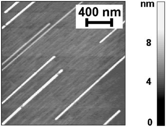
, CdF2 (001)‖Si (111), respectively. On Si (001), CaF2 grew as dots at a low temperature, while at high temperature it grew into wires (Fig. 8). In 1990, Tiwar et al.
Reference Tiwari, Floeder, Blunier, Zogg and Weibel166
used MBE to grow CdTe (100)/BaF2 (100)/CaF2 (100)/Si (100). The substrate temperature was 823 K for CaF2 growth, and CaF2 (100) and Si (100) showed a lattice mismatch of 0.6%. To grow BaF2, the substrate temperature was first set at 823 K and then annealed at 973 K. For growth of CdTe, the substrate temperature was 473–623 K, and CdTe (100) and BaF2 (100) showed a lattice mismatch of 4.5%. RHEED was used to analyze the structure and indicated good crystallinity in the CdTe film.
CaF2 nanowires grown on Si (111) at 700 °C. Reproduced with permission from Ref. Reference Sokolov and Suturin165.

4. Epitaxy on metal halides
Bujor et al. Reference Bujor and Vook167 used PVD to grow CaF2 on NaCl (100). They found that at 623 K, epitaxy was observed with CaF2 (100)‖NaCl (100) and CaF2 〈110〉‖NaCl 〈100〉; at 473 K, the epitaxy was revealed as: CaF2 (110)‖NaCl (100) and CaF2 〈111〉‖NaCl 〈100〉. These epitaxy results were successfully explained with a hard-sphere model.
D. Zincblende structure
1. Epitaxy on III–V compounds
Metal halide with zincblende structure is not populous. Reference Tong, Snyder, Stanley Williams, Yanase, Segawa and Anderson168 Typical ones are copper-based. In 1992, Chen et al. Reference Chen, Dumas, Ahsan, Kahn, Duke and Paton169 successfully applied PVD to grow epitaxial CuCl (110) on GaP (110). The substrate temperature was 373 K and the lattice mismatch was 0.8%. Later, Wake et al. Reference Wake, Saiki and Koma170 used PVD to grow CuX (X = Cl, Br, I) on GaAs (111) and GaAs (110). They found that when an interface had only covalent bonds, to realize epitaxy growth, a rigid lattice match relation between the substrate and film was required. Surface reconstructions occurred to relax the strain because of strong and directional features of covalent bonds. When an interface had only ionic bonds, however, it was found that epitaxy growth could be achieved even with a large lattice mismatch. The Phillips’s ionicity of CuX is 0.692–0.746, which Cu-X bonds have both covalent and ionic characters. It was found that CuX was reconstructed to replicate the GaAs surface structure, and an epitaxy growth was achieved though the lattice mismatch between film and substrate is large.
2. Epitaxy on oxide substrates
In 1990s, Yanase et al.
Reference Yanase and Segawa171–Reference Yanase, Segawa, Mihara, Tong and Williams174
used MBE to grow CuCl on MgO (001). The substrate temperature was between 333 and 353 K. The orientation relationships were CuCl (111)‖MgO (001) and CuCl
 $\left[ {\bar 110} \right]$
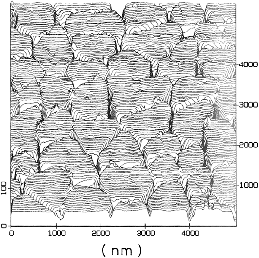
‖MgO [110]. It was found that CuCl on MgO (001) first formed triangular islands and then became hexagonal-shaped islands (Fig. 9). They attributed this kind of growth to the rapid diffusion of CuCl on MgO (001) because of excessive CuCl. At the same time, Wu et al.
Reference Wu, Guo and Møller175
achieved the epitaxial growth of the CuCl film on TiO2 (110) via PVD with the substrate at room temperature.
AFM image of CuCl film grown on MgO (001). Reproduced with permission from Ref. Reference Yanase and Segawa171.

E. Layered structure
1. Epitaxy on layered-structure substrates
Often to grow layered metal halides, substrates with a layered structure are preferred
Reference Ai, Guan, Li, Yao, Chen, Zhang, Duan and Duan176–Reference Ha, Liu, Zhang, Giovanni, Sum and Xiong178
(Fig. 10). In 1987, Nagamune et al.
Reference Nagamune, Takeyama, Miura, Minagawa and Misu179
attempted the epitaxial growth of Pbl2 on CdI2 (001). The substrate temperature was 348–393 K. The lattice mismatch was 7.8% between CdI2 and PbI2. They attributed the successful epitaxial growth to weak van der Waals interaction. In 1990s, many studies were carried to epitaxially grow layered metal halides on layered substrates. Ueno et al.
Reference Ueno, Yamamoto, Saiki and Koma180
used MBE to grow layered metal halides (PbI2, CdI2) on different kinds of layered substrates including MoS2 (0001), MoSe2 (0001), NbSe2 (0001), TaSe2 (0001), GaSe (0001), and Se-GaAs
 $\left( {\bar 1\bar 1\bar 1} \right)$
. RHEED was introduced to analyze structures of thin films. Substrate temperature was at 150 °C. They concentrated on the growth of PbI2 and found the epitaxial relations as: PbI2 (0001)‖MoS2 (0001) and PbI2
 $\left[ {2\bar 1\bar 10} \right]$
‖MoS2
 $\left[ {10\bar 10} \right]$
, PbI2 (0001)‖MoSe2 (0001) and PbI2
 $\left[ {2\bar 1\bar 10} \right]$
‖MoSe2
 $\left[ {10\bar 10} \right]$
or MoSe2
 $\left[ {2\bar 1\bar 10} \right]$
, PbI2 (0001)‖NbSe2 (0001) and PbI2
 $\left[ {2\bar 1\bar 10} \right]$
‖NbSe2
 $\left[ {2\bar 1\bar 10} \right]$
with 19° offset, PbI2 (0001)‖TaSe2 (0001) and PbI2
 $\left[ {2\bar 1\bar 10} \right]$
‖TaSe2
 $\left[ {2\bar 1\bar 10} \right]$
with 19° offset, PbI2 (0001)‖GaSe (0001) and PbI2
 $\left[ {2\bar 1\bar 10} \right]$
‖GaSe
 $\left[ {2\bar 1\bar 10} \right]$
, and PbI2 (0001)‖GaSe (0001) and PbI2
 $\left[ {2\bar 1\bar 10} \right]$
‖GaSe
 $\left[ {2\bar 1\bar 10} \right]$
, despite large lattice mismatches of 44%, 38%, 32%, 31%, 21%, and 14%, respectively. Meanwhile, Kurisu et al.
Reference Kurisu, Yamamoto, Sueoka and Matsuura181
achieved the epitaxial growth of PbI2–CdI2 superlattices on mica and/or sapphire. Recently, Wang et al.
Reference Wang, Sun, Zhang, Lu and Shi182
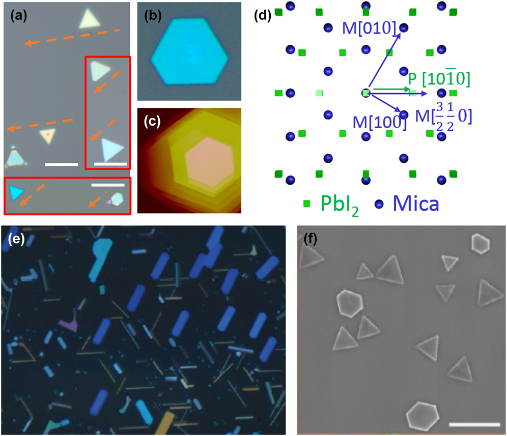
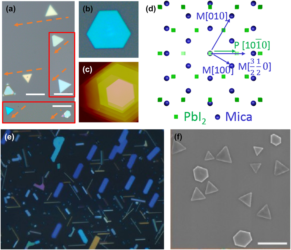
applied CVD to grow PbI2 flakes on mica [Figs. 10(a)–10(d)]. The substrate temperature was 523–573 K. The epitaxial relation was proposed to be PbI2 [0001]‖mica [001] with 5° offset and PbI2
 $\left[ {10\bar 10} \right]$
‖mica [310].
(a–e) PbI2 flakes grown on mica. (f) CdI2 flakes on SiO2. Reproduced with permission from Refs. Reference Ai, Guan, Li, Yao, Chen, Zhang, Duan and Duan176, Reference Ha, Liu, Zhang, Giovanni, Sum and Xiong178, and Reference Wang, Sun, Zhang, Lu and Shi182.
In addition to CdI2 and PbI2, in 1990, Takeyama et al. Reference Takeyama, Watanabe, Ichihara, Suzuki and Miura183 used a hot wall method to grow BiI3 on PbI2 (001) and CdI2 (001) substrate. The substrate temperature was 293 K–363 K, respectively. Epitaxy was achieved though large in-plane lattice mismatches that existed, BiI3 on PbI2 (001): 39% and BiI3 on CdI2 (001): 43%.
2. Epitaxy on III–V compounds
In 1990, Mowbray et al. Reference Mowbray and Jones184 achieved the epitaxial growth of CdI2 on InSb (001) via PVD with the substrate temperature at 310 K. The epitaxial relation was found as CdI2 (0001)‖InSb (001).
F. CsCl structure
1. Epitaxy on oxide substrates
For the CsCl structure, the metal halide is mainly focused on Cs-based compounds. In 1999, Suzuki et al. Reference Suzuki and Souda185 realized the epitaxial growth of CsCl on MgO (001) by PVD. The substrate was gradually heated from 293 to 673 K. The epitaxial relations were (001) α-CsCl‖(001) MgO & [100] α-CsCl‖[100] MgO, (001) β-CsCl‖(001) MgO & [110] β-CsCl‖[100] MgO. The lattice mismatch between α-CsCl and MgO is 2.1%.
2. Epitaxy on metal halides
Common substrates for CsCl-type metal halide film growth are metal halides themselves. In 2003, Yoshikawa et al. Reference Yoshikawa, Kiguchi, Ueno, Koma and Saiki186 used MBE to grow CsCl on GaAs (001). At 470 K, the epitaxial relation was found as CsCl (001)‖GaAs (001) and [100] CsCl‖[100] GaAs. At the same time, Kiguchi et al. Reference Kiguchi, Entani, Saiki and Koma187 applied MBE to grow CsBr on LiF (001) and KBr (001). They found that, on LiF (001), at 300 K, α-CsCl was formed and had an epitaxial relation of (110) α-CsBr‖(001) LiF and [001] α-CsBr‖[001] LiF. At 400 K, β-CsCl was formed and had an epitaxial relation of (001) β-CsBr‖(001) LiF and [100] β-CsBr‖[100] LiF. On KBr (001), however, at 300–500 K, only β-CsCl was observed with an epitaxial relation of (001) β-CsBr‖(001) KBr and [100] β-CsBr‖[100] KBr.
G. Perovskite structure
1. Epitaxy on layered substrates
Most studies on the vapor phase epitaxy of metal halide perovskites were carried very recently and the substrate was focused on layered materials. In 2015, Wang et al. Reference Wang, Shi, Xin, Lian and Shi188 applied CVD to grow MAPbCl3 films (MA– = CH3NH3–) on mica [Figs. 11(a)–11(d) and 11(g)–11(i)]. TEM and AFM were used to analyze the structure of films. The epitaxy relation was found as mica (001)‖MAPbCl3 (001), mica (200)‖MAPbCl3 (200) (with 5° offset), and mica (020)‖perovskite (010) (with 5° offset). They also developed a new model to analyze the kinetics in van der Waals epitaxy. With this model, they explained the 2D-layered growth of 3D-structured MAPbCl3, combined with a Monte Carlo simulation. In 2016, Zhang et al. Reference Zhang, Su, Liu, Xing, Sum and Xiong189 used a same CVD method and successfully grew high-quality epitaxial CsPbX3 sheets (X = Cl, Br, I) on muscovite mica [Figs. 11(e)–11(f)].
(a–d) Hybrid perovskite sheets grown on mica. (e, f) Inorganic perovskite sheets on mica. (g–i) Epitaxial model between perovskite and mica. Reproduced with permission from Refs. Reference Wang, Shi, Xin, Lian and Shi188 and Reference Zhang, Su, Liu, Xing, Sum and Xiong189.

In addition to nanosheets, the nanowire morphology epitaxially grown on certain substrates was also realized recently. In 2016, Wang et al. Reference Wang, Sun, Shivanna, Yang, Chen, Guo, Wang, Wertz, Deschler, Cai, Zhou, Lu and Shi190 used CVD to grow CsPbX3 (X = Br, I) nanowires on mica with the substrate temperature at 673 K [Figs. 12(a)–12(c)]. A large scale of aligned nanowires with 3-fold in-plane symmetry was observed. The epitaxial relation was CsPbX3 (011)‖mica (001) and CsPbX3 (100)‖mica (020) with a 30° offset. Almost at the same time, Chen et al. Reference Chen, Fu, Samad, Dang, Zhao, Shen, Guo and Jin191 applied a similar method for the growth of CsPbX3 (X = Cl, Br, I) nanowires on mica and found the same epitaxial relations [Fig. 12(d)]. Besides the inorganic halide perovskites, their hybrid counterparts have also been achieved epitaxially. In 2017, Wang et al. Reference Wang, Chen, Deschler, Sun, Lu, Wertz, Hu and Shi192 demonstrated the growth of MAPbI3/MAPbBr3 nanowires double heterojunction on mica by vapor phase epitaxy [Figs. 12(e) and 12(f)]. It was found that the growth temperature for the hybrid system was slightly lower than their pure inorganic systems.
Perovskite halide nanowires on mica. (a–d) Inorganic perovskite. (e, f) Hybrid perovskite. Reproduced with permission from Refs. Reference Wang, Sun, Shivanna, Yang, Chen, Guo, Wang, Wertz, Deschler, Cai, Zhou, Lu and Shi190, Reference Chen, Fu, Samad, Dang, Zhao, Shen, Guo and Jin191, and Reference Wang, Chen, Deschler, Sun, Lu, Wertz, Hu and Shi192.

IV. SUMMARY
In summary, this review comprehensively covers the major physical properties of general metal halide materials: photodecomposition, ionic conducting, ferroelectricity, Rashba splitting, magnetic properties, optoelectronic/electro-optic properties, electron beam-induced decomposition, superconductivity, chemical adsorption-induced electrical conductivity modification, and radiation-induced electrical conductivity change. It also thoroughly covers the major progresses in the vapor phase epitaxial growth of metal halide materials with CsCl structure, fluorite, layered, zincblende, wurtzite, rocksalt, and perovskites. In the vapor phase epitaxy, important parameters/growth results such as substrate temperatures, epitaxial relations, substrate selections, and growth morphologies are discussed. It is our hope that this review could be helpful in inspiring the discovery of new properties or designing growth parameters for emerging metal halide crystals.
ACKNOWLEDGMENTS
Y.H., Y.W., Z.C., E.W., and J.S. are supported by NSF Awards under CMMI 1550941 and CMMI 1635520. X.S. is supported by the NYSTAR Focus Center at RPI, C130117.