Introduction
Due to the high integration of substantial components, electromagnetic interference unavoidably exists in radio frequency (RF) front-end system. To address this problem, differential routing as an effective method is widely-used. Since there is always some imbalanced factors such as unbalanced routing, amplitude difference, patterned ground plane and clock skew, vast common-mode (CM) noise suppression technologies have been developed. Although these designs guarantee the integrity of the differential-mode (DM) signals, they are the main sources of radiation when coupled to adjacent radiators. To immune from reflection, absorptive filters have attracted people’s interest [Reference Morgan and Boyd1–Reference Deng, Ma, Wang, Wang, Li and Zhao8].
Nowadays, there are two mainstreams of reflectionless topologies: one is the symmetric reflectionless network topology based on odd-/even-mode circuit, which can inhibit reflection at both passband frequency and stopband frequency [Reference Hsiao, Cheng and Wu9–Reference Zhu, Song, Fan, Guo, Zhou and Fan12]. The second type is the reflectionless topology based on complementary duplex system, which is generally analyzed by coupling matrix [Reference Gómez-García, Muñoz-Ferreras and Psychogiou13–Reference Psychogiou and Gómez-García16]. Further improvements on performance emerge continuously. The power divider proposed in paper [Reference Zhao, Wei, Yang and Gómez-García17] exhibits high suppression level of CM signals by defecting slotlines on the ground plane, while only DM input reflectionless behavior is achieved and the CM signals maintains reflective. For performance upgradation, the techniques in paper [Reference Hsiao, Cheng and Wu9] extent to two-port reflectionless, while other filters can achieve CM and DM absorption simultaneously [Reference Zhao, Wei, Malki, Yang and Gómez-García18–Reference Zhang, Wu, Wang and Yan20]. The design in paper [Reference Zhou, Zhao, Xu, Li, Shi and Yin21] absorbs the energy by the inherent conductor and dielectric loss instead of loading resistors. However, the measured reflectionless performance varies considerably with the simulation results and seems to be unstable.
The half-wavelength ring resonator has been investigated in papers [Reference Zhang, Wu, Wang and Yan20] and [Reference Feng, Che, Ma and Xue22]. This paper further presents a simpler absorptive structure based on the half-wavelength ring resonator, which makes it easier for practical fabrication. The analysis of DM/CM equivalent circuit is given. The design procedures are introduced. The measured results verify its ability of eliminating undesired signals. Specifically, the proposed balanced reflectionless filter exhibits excellent DM matching level, CM suppression level, and wideband reflectionless bandwidth.
Theoretical analysis
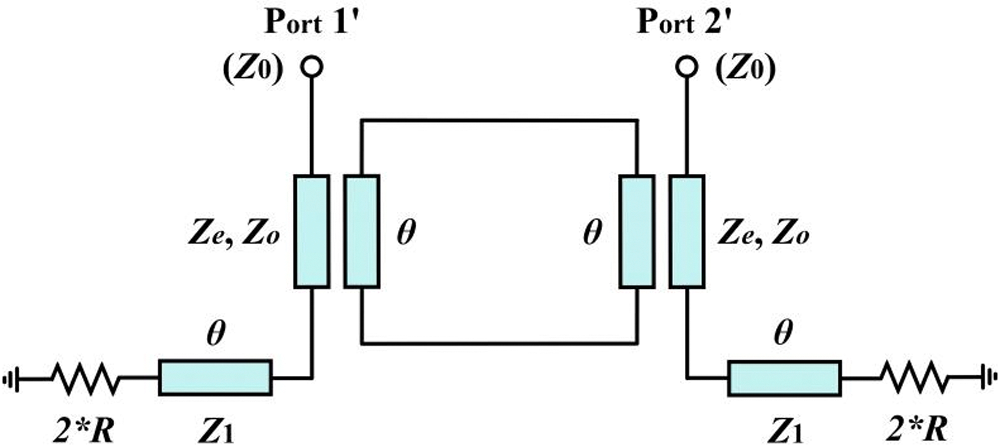
As shown in Fig. 1, the proposed balanced reflectionless filter is composed of a half-wavelength ring resonator (formed by four quarter-wavelength coupled lines, Ze, Zo, θ), four quarter-wavelength lines (Z 1, θ), and two absorptive resistors (R). The quarter-wavelength lines are connected at the end of the half-wavelength ring resonator. Two lumped resistors are placed along the symmetric line.
The schematic of the proposed balanced reflectionless filter.

DM/CM equivalent circuit analysis
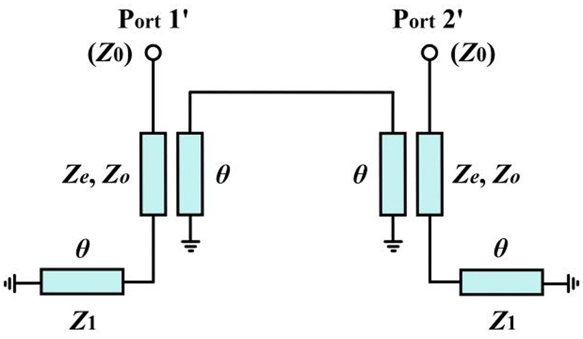
Under the excitation of DM signals, a virtual short appears along the symmetric line as in Fig. 2. Then, the odd-/even- mode equivalent circuits for the DM are obtained in Fig. 3.
The DM equivalent circuit of the proposed balanced reflectionless filter.

The (a) odd-mode, and (b) even-mode equivalent circuits for DM circuit.

According to the voltage/current relationship, the input impedances Zino,DM, Zine,DM are derived as follow:
 \begin{equation}{Z_{ino,DM}} = \frac{{4 + 2{Z_1}({Z_e} + {Z_o})}}{{ - ({Z_e} + {Z_o})\left[ {{Z_{in1}}({Z_e} + {Z_o}) + j2\cot \theta } \right]}}\end{equation}
 \begin{equation}{Z_{ine,DM}} = \frac{\begin{array}{l}{a^2}({a^2} - {b^2} - {c^2} - {d^2}) + 2abcd + (2{a^3} - a{b^2} \\[4pt] \qquad - 2a{c^2} - a{d^2} + 2bcd){Z_{in1}} + ({a^2} - {c^2}){Z_{in1}^2}\end{array}}{{(a + {Z_{in1}})({a^2} + a{Z_{in1}} - {b^2})}}\end{equation}
where
 \begin{equation}a = - j\frac{{{Z_{e1}} + {Z_{o1}}}}{2}\cot \theta \end{equation}
 \begin{equation}b = - j\frac{{{Z_{e1}} - {Z_{o1}}}}{2}\cot \theta \end{equation}
 \begin{equation}c = - j\frac{{{Z_{e1}} - {Z_{o1}}}}{2}\csc \theta \end{equation}
 \begin{equation}d = - j\frac{{{Z_{e1}} + {Z_{o1}}}}{2}\csc \theta \end{equation}
 \begin{equation}{Z_{in1}} = j{Z_1}\tan \theta \end{equation}
To realize the passband of DM signals, S dd11 = 0 needs to be met. Therefore, one transmission pole can be obtained by imposing Zino,DM × Zine,DM = Z 02 [Reference Matthaei, Young and Jones23]:
 \begin{equation}{\theta _{TP1}} = \frac{\pi }{2}\end{equation}
Under the excitation of CM signals, a virtual open appears along the symmetric line as in Fig. 4. Then, the odd-/even- mode equivalent circuits for the CM are obtained in Fig. 5. The input impedances Zino,CM, Zine,CM are derived as
 \begin{equation}{Z_{ino,CM}} = \frac{{4{Z_e}^2{Z_o}^2 - j2{Z_{in2}}{Z_e}{Z_o}({Z_e} + {Z_o})\cot \theta }}{{{Z_{in2}}{{({Z_e} + {Z_o})}^2} - j2{Z_e}{Z_o}({Z_e} + {Z_o})\cot \theta }}\end{equation}
 \begin{equation}{Z_{ine,CM}} = \frac{{{{({Z_e} + {Z_o})}^2} - j2{Z_{in2}}({Z_e} + {Z_o})\cot \theta }}{{4{Z_{in2}} - j2({Z_e} + {Z_o})\cot \theta }}\end{equation}
The CM equivalent circuit of the proposed balanced reflectionless filter.

The (a) odd-mode, and (b) even-mode equivalent circuits for CM circuit.

where
 \begin{equation}{Z_{in2}} = \frac{{(2R + j{Z_1}\tan \theta ){Z_1}}}{{{Z_1} + j2R\tan \theta }}\end{equation}
To meet S cc21 = 0, Zino,CM = Zine,CM should be satisfied [Reference Matthaei, Young and Jones23]. Two transmission zeros are obtained as
 \begin{equation}{\theta _{TZ1}} = 0,{\theta _{TZ2}} = \pi \end{equation}
To enhance CM absorption, S cc11 = 0 should be satisfied. By imposing Zino,CM × Zine,CM = Z 02 [Reference Hsiao, Cheng and Wu9], the value R of resistor is extracted as
 \begin{equation}R = \frac{{{Z_1}^2{Z_0}}}{{2{Z_e}{Z_o}}}\end{equation}
Proposed balanced reflectionless filter
Figure 6 illustrates the influences of the coupling coefficient k (k = [(Ze-Zo)/(Ze + Zo)]) on the proposed filter. As k increases, the bandwidth and the selectivity for DM improves, whereas the out-of-band rejection decreases. The two transmission zeros aside the passband slightly moves as k changes. It indicates that k affects more on the DM bandwidth. On the other hand, as k increases, the CM reflectionless bandwidth remains relatively stable, while the absorption around center frequency gets enhanced. For S cc21, the suppression level is gradually decreased. The two transmission zeros fixedly locate at DC and 2f 0, which only depends on the center frequency and hardly influence the CM bandwidth. Therefore, the value of k for the half-wavelength ring resonator should be carefully designed to achieve initial response at first. Then, Z 1 needs to be adjusted to further realize satisfied DM passband and CM suppression performances. Ultimately, the R value can be determined using equation (10) to effectively absorb CM noise.
The (a) DM, (b) CM responses of the proposed filter with k (k 1 = 0.29: ze = 100 Ω, zo = 55 Ω; k 2 = 0.38: ze = 107 Ω, zo = 48 Ω; k 3 = 0.47: ze = 110 Ω, zo = 40 Ω).

To provide specific guidelines, designing the proposed reflectionless filter requires following procedures: (1) Select center frequency f 0 and determine the demanded bandwidth; (2) Choose proper impedance (Ze, Zo, Z 1) of the transmission lines and adjust to obtain fundamental property; (3) Derive the resistor value R to achieve CM suppression and absorption properties; (4) Obtain layout dimensions and realize physically; (5) Optimize the layout parameters. Moreover, tight coupling is needed for this design that the spacing between coupled lines is relatively small, which requires higher processing capability. Through optimization, the final circuit parameters are: Ze = 107 Ω, Zo = 48 Ω, Z 1 = 84 Ω, Z 0 = 50 Ω, R = 50 Ω, θ = 90°.
Experimental results and discussion
For verification, a prototype with f 0 = 2.2 GHz is fabricated on the substrate (εr = 2.65, h = 1.0 mm, tan δ = 0.002). Figure 7 shows the layout and the photograph of the proposed balanced reflectionless filter. As can be seen, the experimental results are in good agreement with the full-wave simulated results.
The (a) layout and (b) photograph of the fabricated prototype.

Figure 8(a) indicates that DM 3-dB bandwidth can reach up 0.65 GHz (1.85–2.5 GHz, 0.3f 0). One transmission pole is generated in passband, locating at 2.2 GHz. The 27-dB upper stopband is achieved from 3 to 5.95 GHz (2.7f 0). Figure 8(b) presents the CM properties. An all-stop behavior is realized that |S cc21| within a measurable range (DC to 8 GHz, 3.64f 0) is higher than 17.8 dB. Furthermore, |S cc21| from DC to 6 GHz (2.73f 0) is higher than 21.6 dB, exhibiting excellent CM noise suppression performance. The 10-dB reflectionless bandwidth is 4.3 GHz (|S cc11| from DC-4.3 GHz is higher than 10 dB, 1.95f 0). The absorption efficiency is defined as 1—|S cc21|2—|S cc11|2. Over DC-4.4 GHz (2f 0), the absorption efficiency is higher than 80%. The effective size of the proposed balanced reflectionless filter covers 39.4 mm × 39.4 mm (0.38λg × 0.38λg, λg denotes the guided wavelength at 2.2 GHz).
The (a) DM, (b) CM responses of the proposed balanced reflectionless filter.

Table 1 compares the proposed balanced reflectionless filter with former related studies. Although the designs in papers [Reference Psychogiou and Gómez-García16] and [Reference Feng, Che, Ma and Xue22] exhibit the highest suppression level, the DM insertion loss is really high. In this work, the DM insertion loss, the upper stopband are superior to other designs. In addition, the proposed structure shows excellent DM matching level, CM mismatch level, and wideband reflectionless bandwidth. Besides, the CM absorption behavior is achieved, the DM stopband signals remains an unsolved issue and will be investigated in the future. Generally, for such kind of ACMF, people are more focused on CM noise absorption. If DM stopband signals needed to be absorbed, the structure tends to be much more complicated [Reference Feng, Che, Ma and Xue22]. It seems that simple structure and desired performance are difficult to obtain at the same time. In this paper, we aim to get wideband CM reflectionless bandwidth with a simple structure.
Comparison with published balanced reflectionless filters

DM IL = differential-mode insertion loss; 3-dB DM BW = 3-dB differential-mode bandwidth; 10-dB CM ABW = 10-dB common-mode absorption bandwidth; N.A. = not available.
a Estimated from graph.
Conclusion
This paper presents a simpler absorptive structure based on the half-wavelength ring resonator, which makes it easier for practical implementation. The analysis of DM/CM equivalent circuit is given. The design procedures are introduced. A circuit sample is fabricated. The measured results verify its ability of eliminating undesired signals. Specifically, the proposed balanced reflectionless filter exhibits excellent DM matching level, CM suppression level, and wideband reflectionless bandwidth.
Acknowledgments
This work was supported by the Fundamental Research Funds for the Central Universities (D2230240), the National Natural Science Foundation of China (62231014, 62321002, U23A20288), and the Natural Science Foundation of Guangdong Province (2024A1515011726, 2022A1515110226, 2024A1515011982).
Competing interests
The authors report no conflict of interest.

Yijun Weng was born in Shangrao, Jiangxi, China, in 1999. She received the B.Sc. degree from Changan University, Xian, China, in 2021. She is currently pursuing M.S. degree and Ph.D. degree in microwave technique at South China University of Technology, Guangzhou. Her current research interests include wideband circuits and technologies, microwave and millimeter-wave circuits and components.

Pei Qin received the B.Sc. degree in electronic science and technology from the University of Electronic Science and Technology of China, Chengdu, China, in 2010, and the Ph.D. degree in electronic engineering from the City University of Hong Kong, Hong Kong, in October 2016. From November 2016 to February 2022, she was a Senior IC Design Engineer with HiSilicon, with focusing on all digital phase-locked loop (ADPLL) IC design. In March 2022, she joined the South China University of Technology, Guangzhou, China, where she is currently an Associate Professor. She is now working on the research areas of analog/RF front-end and phase-locked loop (PLL) integrated circuit design.

Wenjie Feng was born in Shangqiu, Henan, China, in 1985. He received the B.Sc. degree from the First Aeronautic College of the Airforce, Xinyang, China, in 2008, and the M.Sc. and Ph.D. degrees from the Nanjing University of Science and Technology (NUST), Nanjing, China, in 2010 and 2013, respectively.
From July 2017 to September 2017, he was a Research Fellow with the City University of Hong Kong. From October 2010 to March 2011, he was an Exchange Student with the Institute of High Frequency Engineering, Technische Universität München, Munich, Germany. He is currently a Professor with South China University of Technology, Guangzhou, China. He has authored or coauthored over 120 IEEE journal articles (including 80 IEEE TRANSACTIONS papers) and 80 conference papers. His research interests include wideband circuits and technologies, microwave and millimeter-wave circuits and components, circuit interconnection, and packaging.
Dr. Feng was a recipient of the National Science Fund for Excellent Young Scholars in 2018, the Young Scientist Award of ACES-China 2018, and a reviewer for over 20 internationally refereed journals and conferences. He currently serves as an Associate Editor for IET Microwaves, Antennas & Propagation, IET Electronics Letters and International Journal of Electronics.