I. INTRODUCTION
Chalcopyrite solar cells have recently reached a new record efficiency of 22.6%, 1 thus demonstrating the continuous improvement of this technology. Furthermore, Cu(In,Ga)Se2 (CIGSe) polycrystalline thin-film solar cells stand out due to their high stability and tolerance against environmental influences e.g., shading or cosmic radiation. Reference Morioka, Shimazaki, Kawakita, Imaizumi, Yamaguchi, Takamoto, Sato, Ohshima, Nakamura, Hirako and Takahashi2 With an additional short energy payback time they constitute a serious thin-film competitor for wafer-based silicon solar cells. When envisaging a high production volume, however, the scarcity of the contained element indium can become a limiting factor. This consideration and the high supply risk of In [8.1/10 in 2015 (Ref. 3)] need to be addressed by a reduction of absorber material usage. Reduced material consumption will also help to further reduce costs, since material consumption still contributes to more than 60% of production costs. Reference Palm, Karg, Schneider, Kushiya, Stolt, Tiwari, Niemi, Beck, Eberspacher, Wohlfart, Bayman, Schoop, Wieting, Ramanathan, Dimmler, Kuhn, Whitelegg, Rühle, Lincot, Naghavi, Walter, Schlatmann, Lux-Steiner, Kuypers, Szyszka, Siebentritt, Lechner, Powalla, Noufi and Schock4 When approaching the material reduction by reducing the absorber thickness from typical values of 2–3 µm to below 500 nm, a further benefit will lie in an increasing production throughput. Apart from these economic aspects, thin absorbers are beneficial for reduced recombination in the bulk. On the other hand, they bring the challenges of more serious interface recombination and in particular incomplete absorption. We will focus on the optical aspect and investigate how the absorption of ultrathin CIGSe solar cells can be enhanced by integrating nanoparticles.
Nanoparticles for absorption enhancement have been successfully applied in various types of solar cells and there are numerous examples for integration in amorphous silicon, crystalline silicon, or organic devices. Reference Gu, Ouyang, Jia, Stokes, Chen, Fahim, Li, Ventura and Shi5 Metal nanoparticles were initially in focus due to their plasmonic effects allowing for strong light interaction. Reference Pillai, Catchpole, Trupke and Green6 Large-angle scattering, strong near-fields and coupling into waveguide modes are the prominent effects. Reference Atwater and Polman7 Despite these advantages, the parasitic absorption of metal nanoparticles and their limited chemical stability are serious drawbacks which make dielectric particles favorable. Reference Ott, Ring, Yin, Calvet, Stannowski, Lu, Schlatmann and Ballauff8 These are characterized by the absence of parasitic absorption and high thermal stability (inorganic dielectrics). At the same time they also give rise to resonant modes like Mie resonances Reference van Lare, Lenzmann and Polman9 or whispering gallery modes. Reference Grandidier, Weitekamp, Deceglie, Callahan, Battaglia, Bukowsky, Ballif, Grubbs and Atwater10 As a unison between metals and dielectrics, core-shell nanoparticles are an option to exploit beneficial effects from both materials. Reference Schmid, Tsakanikas, Mangalgiri, Andrae, Song, Yin, Riedel and Manley11
In this paper, we evaluate the potential of integrating metallic, metal-dielectric core-shell, and fully dielectric nanoparticles in ultrathin chalcopyrite solar cells for absorption enhancement. For different integration positions within the solar cell structure, theoretical expectations and potential benefits are presented. These are always balanced against experimental challenges arising for particular geometries due to the very specific fabrication processes of CIGSe solar cells. We will summarize the geometries which have proven beneficial for other types of solar cells and elaborate on why or why not they are equally applicable for chalcopyrite-based devices. In this way, we will identify the most promising configurations for ultrathin CIGSe solar cells.
II. METHODS
A. Theoretical
Numerical calculations were carried out using the finite-element method. This approach solves partial differential equations, here Maxwell's equations, using a variational approach and a set of basis functions which are locally defined on domain elements. The computational domain is divided into small, so called finite elements with sizes adjustable to precisely fit the shapes of the geometry. In our simulations, either isolated particles at interfaces or hexagonally arranged periodic particles in a chalcopyrite solar cell structure were investigated.
For the case of an isolated particle all outer boundaries were set to be perfectly matched layers (PML) and the scattered field was calculated. The absorption and scattering behavior is expressed in the parameters absorption cross-section C abs, scattering cross-section in transmission C scaT, and in reflection C scaR. These values have been normalized to the geometric cross-section of the particle given by πr 2, r being the radius of the particle. For isolated nanoparticles additionally the angular distribution function (ADF) of the scattered light can be extracted from the far-field. To probe far-field properties, the absorption of the surrounding media was set to zero.
For the nanoparticles integrated into the solar cell stack, periodic boundary conditions were chosen on the sides of the hexagonal unit cell in which the nanoparticle was centered and PMLs were used in the incident and outgoing light directions. In this full field calculation transmission T, reflection R and absorption A CIGSe were the parameters extracted. The pitch between the particles was varied by a multiple m of the particle diameter with an additional 10 nm avoiding contact between particles. For the contour plots presenting T, R, or A CIGSe as a function of m and r, the wavelength dependent curves were multiplied with the solar spectrum and the energy per photon and then integrated over the wavelength range from 300 to 1200 nm leading to values in units of short circuit current density (mA/cm2). The position of the nanoparticles was varied between different interfaces of the thin-film solar cell structure. In the case of integration at an interior interface, the thickness of the incorporating layer was adapted to compensate for the nanoparticle volume. The primary thin-film stack was air/ZnO:Al (AZO)/i-ZnO/CdS/CIGSe/Mo from top to bottom with typical thicknesses of 240, 130, 50, and 400 nm for AZO, intrinsic ZnO (i-ZnO), CdS, and CIGSe for an ultrathin chalcopyrite solar cell. As an alternative to the opaque Mo back contact a transparent conductive oxide like In2O3:Sn (ITO) can be chosen. In this case the interface to the glass substrate needs to be considered as well.
Since nanoparticles prepared by chemical methods (see below) are most easily obtainable in a spherical shape, spheres were used in our basic theoretical investigations. For better comparability between the simulation results, this shape was maintained for the various integration positions despite the reality that deposition on a substrate will tend to distort the nanoparticle shape. We will briefly address the influence of contact angle; however, the focus is rather aimed at a fundamental theoretical understanding of the mechanisms, which are within a certain range largely independent for different contact angles.
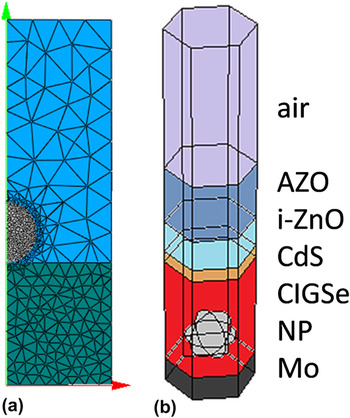
Figures 1(a) and 1(b) show examples of the computational structure of an isolated nanoparticle at an interface and of a nanoparticle integrated into the solar cell structure, respectively. The software tools we used were JCMsuite 12 and Comsol Multiphysics. 13 The refractive index data of the thin films were extracted from transmission and reflection measurements of individual layers using the software RefDex. Reference Yin, Manley and Schmid14,15 For the metallic nanoparticles Ag as the most promising plasmonic material in the visible was chosen with refractive index data from Palik. Reference Palik16 For the dielectric nanoparticles a refractive index of 1.46 was set, which equally corresponds to polystyrene (PS) or SiO2. In the electric field maps shown throughout the paper, the plane of polarization is represented.
Simulation structure. (a) Nanoparticle at interface (exemplarily Ag nanoparticle in air to AZO) for calculation of absorption and scattering cross-sections—PML surrounding not shown (JCMsuite), (b) nanoparticle integrated into the CIGSe solar cell structure [exemplarily SiO2 nanoparticle (NP) in CIGSe to Mo] for extraction of absorption and reflection—PML top and bottom layer not shown (Comsol).

B. Experimental
The experimental structure of the chalcopyrite solar cell is AZO/i-ZnO/CdS/CIGSe/Mo/glass. Also here ITO can be chosen as a transparent back contact replacing Mo. Mo or ITO was deposited by sputtering and had a thickness of 800 nm or 200 nm, respectively. The ultrathin CIGSe absorber of less than 500 nm thickness was grown in a three-stage co-evaporation process at maximum temperatures between 440 and 600 °C. Reference Yin, Brackmann, Hoffmann and Schmid17 CdS with a thickness of 50 nm was coated by chemical bath deposition, whereas i-ZnO and AZO with thicknesses of 130 and 240 nm, respectively, were again sputtered. Finally, Ni/Al grids were evaporated for front contacting and the solar cells were scribed to areas of 0.5 cm2.
For the fabrication of the nanoparticles, chemical methods were used as a basis. PS or SiO2 spheres were deposited by a self-assembly technique. Reference Kosiorek, Kandulski, Chudzinski, Kempa and Giersig18,Reference Moon, Lee, Kim, Chae, Kim, Kim, Myoung and Jeong19 For this approach, commercially available 20 colloidal solutions of the spheres were suspended in butanol (SiO2) or in ethanol mixed with 1 vol% styrene (PS). The suspension was then brought onto a water surface under which the substrate was submerged. The spheres form a monolayer at the air–water interface, which can be transferred to the substrate by sucking out the water. A two-dimensional closely packed sphere array thus results.
The hexagonally arranged PS or SiO2 spheres can serve directly as a light managing structure. Alternatively, the PS sphere array can be utilized as a mask for material—in our case Ag—deposited on top and filling the gaps in between the spheres. After removing the spheres by toluol, Ag triangles remain which can further be transformed to spheres by annealing at 300 °C for 20 min. The size and spacing of the Ag spheres can be tuned by the size of the template PS spheres and the thickness of the deposited Ag layer. Finally, the spacing between the PS spheres can also be altered by plasma etching in O2 atmosphere. The PS sphere templates can then be used to fabricate SiO2 networks. (Etching SiO2 spheres is in contrast not as easy to handle experimentally as etching PS spheres.)
Au@SiO2 core-shell nanoparticles were synthesized in a three-step process. Gold nanorods were synthesized via the seeded growth method. Reference Wu, Schell, Lublow, Kaiser, Aichele, Schietinger, Polzer, Kühn, Guo, Benson, Ballauff and Lu21 In short, small spherical seeds were formed and added into a growth solution containing the gold precursor (HAuCl4), a mild reducing agent (L-ascorbic acid), and a stabilizing and structure directing surfactant, cetyltrimethylammonium bromide (CTAB). Excess CTAB was removed from the nanorod dispersion via centrifugation. A mesoporous silica shell was then formed via hydrolyzation and condensation reaction of tetraethoxysilane directly on the CTAB-stabilized gold nanorods at pH 10.8. Reference Gorelikov and Matsuura22 After the reaction, the core-shell nanoparticles were washed and redispersed in ethanol via centrifugation. A second dense silica shell was grown onto the mesoporous core-shell nanoparticles to fill the pores and achieve higher thermal stability of the nanorods via the Stöber method in an ethanol/water mixture. Reference Stöber, Fink and Bohn23 The core-shell nanoparticles were redispersed in ethanol and deposited onto the substrates using spin-coating.
The morphology of the thin-film solar cells and the nanoparticles was investigated by scanning-electron microscopy (SEM; Zeiss Leo Gemini 1530, Carl Zeiss AG, Oberkochen, Germany). X-ray photoelectronspectroscopy (XPS) was applied to probe diffusion of material. Optical measurements of transmission and reflection were carried out using a UV–Vis photospectrometer with an integrating sphere (PerkinElmer Lambda 950, PerkinElmer, Rodgau, Germany). Electrical characterization of the solar cells focused on the measurement of external quantum efficiencies (EQE). The EQE was taken in a two-source illumination system with a xenon and a halogen lamp; calibrated Si and Ge diodes were used as references.
III. RESULTS AND DISCUSSION
A. Metallic nanoparticles
1. Integration at front
a. Theoretical
Ag can be seen as the most promising plasmonic material for application in the visible wavelength spectrum. In contrast to materials such as Au, it shows no interband transitions in that wavelength region and compared to non-noble metals like Cu, it gives rise to higher scattering. Reference West, Ishii, Naik, Emani, Shalaev and Boltasseva24,Reference Manley, Burger, Schmidt, Schmid, Sakabe, Lienau and Grunwald25 Additionally, Ag nanoparticles are easy to prepare compared to other materials like Al. Therefore, we perform our investigations of metallic nanoparticles on Ag-based ones.
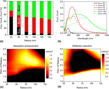
The absorption and scattering cross-section of a nanoparticle are dependent on its radius, which can already be seen in the dipole approximation where C abs ∝ r 3 and C sca ∝ r 6. Reference Bohren and Huffmann26 These proportionalities imply that the scattering cross-section will increase more rapidly than the absorption cross-section for an increasing particle radius. Figure 2(a) visualizes the contribution of absorption and scattering to extinction cross-section C ext = C sca + C abs as a function of particle radius; in addition, scattering in the forwards (C scaT) and backwards (C scaR) direction are separated. A Ag nanoparticle surrounded by air and sitting on AZO was assumed, which corresponds to the front interface of the CIGSe solar cell. As can clearly be seen, the absorption dominates for small nanoparticles and becomes marginal starting from a radius of approximately 75 nm. Absorption is assumed to be lost in the form of heat and therefore called parasitic absorption. A trend toward higher forward scattering can also be observed, yet the difference between C scaT and C scaR is not too distinct. Since for larger particles the center moves further from the interface, backwards scattering of the dipole mode can be enhanced. Note that the values presented were obtained by multiplying the cross-sections with the solar spectrum and integrating over the wavelengths from 300 to 1200 nm.
Theoretical integration of metallic Ag nanoparticles at front (air/AZO) interface. (a) Absorption cross-section C abs and scattering cross-section in backward (C scaR) and forward (C scaT) direction for various radii, (b) C scaT (solid lines) and C scaR (dashed lines) as a function of wave-length for nanoparticle radii of 25, 50, and 75 nm; (c) absorption enhancement in CIGSe as a function of radius and pitch as multiple of diameter, and (d) corresponding reduction in reflection.

Examples of C scaT and C scaR as a function of wave-length are given in Fig. 2(b). Whereas for 25 nm nanoparticle radius the scattering cross-sections are almost negligible, they are significantly greater than unity for large radii. Scattering cross-sections larger than unity signify that the nanoparticle interacts with light from an incident area larger than its geometrical cross-section. This behavior allows for a reduced coverage whilst maintaining full light interaction. A low coverage is highly beneficial for metallic nanoparticles due to their parasitic absorption for small nanoparticles and increasing backwards scattering for larger ones. Looking for example at the r = 75 nm nanoparticle, C scaT = 3 is easily exceeded and we could imagine that a nanoparticle coverage of only one third of the surface area would be sufficient that all incident light will, on average, interact with a nanoparticle. In this case, however, C scaR will not exceed 3 and therefore can be suppressed. When moving on to even larger particles, such as r = 125 nm as depicted further in Fig. 2(b), the peak broadens and the maximum scattering cross-section decreases, which makes it more difficult to deduce a coverage for maximum interaction of C scaT but reduced contribution of C scaR. These observations already point toward the fact that there will be a quite narrow optimum of particle size and coverage for which absorption enhancement can be obtained.
We now move on to consider the integration of the Ag nanoparticles at the front interface of our ultrathin CIGSe solar cell. For the sake of comparability, we continue to assume spherical particles on top of the front AZO layer, although in reality a certain deviation from the spherical shape and a larger contact angle are likely to exist. It should be pointed out that these deviations will influence the scattering curves and results differing to those presented here could easily be obtained for certain configurations. A match with experimental results and an absolute prediction of optimum parameters therefore will require detailed information about the realistic system. Here, we however seek to explain the basic effects that need to be taken into account and evaluate their impact, which is largely independent of contact angle. As we have seen from Fig. 2(a), on the one hand a minimum size of Ag nanoparticles is required for scattering to surpass absorption. On the other hand, drawbacks of larger Ag particles are more pronounced reflection losses which cannot be separated well from transmission by choice of coverage [Fig. 2(b)] and shifting of resonances out of the visible. Therefore, it is not surprising to find a maximum absorption enhancement in a relatively narrow window around the optimum radius and coverage. Figure 2(c) shows a contour image of absorption enhancement in the CIGSe layer as a function of nanoparticle radius and pitch as a multiple of the particle diameter. Pitch instead of coverage was chosen for sake of clarity; due to the dependence on particle radius the two parameters are not simply linearly related. The maximum enhancement of 1.2 mA/cm2 is found for radii around 85 nm and a pitch to diameter ratio of 3. These values match very well with the estimations we made based on calculations of single particles at the air–AZO interface. The low coverage enables the isolated treatment of the nanoparticles for good predictions.
In Fig. 2(d) the reduction in reflection corresponding to Fig. 2(c) is shown, also expressed in terms of short circuit current densities. The color scales are chosen to cover the same absolute range so that reduced reflection and increased absorption can be directly correlated. Notably, a reflection reduction of 1.2 mA/cm2 can be obtained over a much wider parameter space than the absorption enhancement for the same value. This implies the existence of significant losses such that not all of the increase in light incoupling is translated into enhanced absorption in CIGSe. The main source of losses constitute the AZO, i-ZnO, and CdS front contact layers. Due to their parasitic absorption, they will diminish the amount of light reaching the CIGSe absorber layer. Preferential large-angle scattering, which actually is seen as one of the major benefits of plasmonic nanoparticles, cannot be positively exploited: the enhanced path length in the front contact layers will rather increase their parasitic absorption, and as a result of Snell's law, the large scattering angles will have significantly lowered after the light has traversed many successive interfaces on the way to the highest index material CIGSe (for details see also Ref. Reference Yin27). Based on these considerations, obtaining absorption enhancement by integrating metallic nanoparticles at the front interface of ultrathin CIGSe solar cells is highly challenging.
b. Experimental
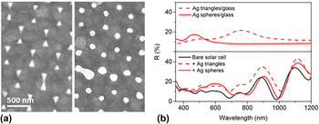
Figure 3(a) shows in SEM pictures the experimental realization of Ag nanoparticles fabricated on top of ultrathin CIGSe solar cells. On the left, Ag triangles are visible which were obtained by depositing 250 nm Ag on top of a 607 nm diameter PS sphere array before releasing the latter one. As can be seen, apart from triangles also some bowties remain. The right part of Fig. 3(a) gives the resulting nanoparticles after subjecting the triangles to a heat treatment at 200 °C for 1 h. Spheres are formed with a radius of approx. 75 nm and a nearest-neighbor distance of 350 nm as resulting from the closely packed PS sphere array. Originating from the bowties, some large particle agglomerates remain and also some small residues around the nanoparticles can be found.
Experimental integration of metallic Ag nanoparticles at front (air/AZO) interface. (a) SEM top view of Ag triangles (left), transformed to Ag nanoparticles (right) on top of a completed ultra-thin CIGSe solar cell; (b) reflection of (top) Ag triangles and spheres on a glass substrate and (bottom) of the same Ag nanostructures on top of the completed solar cell.

Figure 3(b) reveals at the top the reflection of the Ag triangles and spheres deposited for reference on a glass substrate. The resonance is clearly visible with the peak for the Ag triangles being more than 300 nm red-shifted compared to the Ag spheres. Following our theoretical investigations, we would expect these nanostructures to enhance the absorption in an underlying ultrathin CIGSe solar cell. However, the experimental result is not in agreement with these expectations: CIGSe solar cells with Ag nanostructures on top always suffer from deteriorated electrical properties. A detrimental influence of chemical and temperature treatment of the samples as a result of nanoparticle deposition could be excluded by reference experiments. The central drawback of the nanoparticle integration is revealed in the bottom graph of Fig. 3(b): with integrated Ag nanostructures on top, the overall reflection of the ultrathin CIGSe device increases following the resonant behavior of the nanostructures. Thus, the plasmonic resonance cannot be efficiently exploited for coupling light into the CIGSe solar cell structure and the small but theoretically present absorption enhancement cannot be observed.
Metallic nanoparticles added to the front of GaAs or Si solar cells had given the first proof of concept for absorption enhancement from plasmonic nanostructures. Reference Pillai, Catchpole, Trupke and Green6,Reference Derkacs, Lim, Matheu, Mar and Yu28,Reference Nakayama, Tanabe and Atwater29 These structures benefited from the proximity of the nanoparticles to the absorber layer with at maximum a spacer layer of a few tens of nanometers. Scattering and also near-field coupling could be directly exploited and losses minimized. In CIGSe solar cells, however, the thick front contact layers, totaling several hundred nanometers, separate the nanoparticles from the absorber. Losses are considerable and the positive impact of nanostructures on top of the completed device is significantly reduced.
2. Integration at back
a. Theoretical
The parasitic absorption and high reflectivity of metal nanoparticles suggests that integration at a rear interface of the solar cell structure may be more favorable. In this way, light will have once passed the absorber which will naturally filter out the short wavelengths from interacting with the nanoparticles. Thus, the losses in absorption by the nanoparticles can be suppressed. The reflectivity can be fully exploited since plasmonic particles are dominated by the electric dipole mode which scatters more strongly toward the material of higher refractive index. This can be understood via total internal reflection of scattered beams at the interface causing light to be trapped inside the higher refractive index material, which is formally covered by exploitation of the reciprocity theorem in Ref. Reference Mertz30.
Before looking into the scattering behavior of the Ag nanoparticles at the back, we need to decide which interface to choose. For full exploitation of scattering and a large angular distribution, a close contact to the absorber layer would be desirable. However, Ag can be built into the chalcopyrite structure forming (Ag,Cu) (In,Ga)Se2 (Ref. Reference Boyle, McCandless, Hanket and Shafarman31) and therefore the nanoparticles are not considered to be stable in direct contact with the absorber. Thus, at least one intermediate layer should be present, which at the same time provides electrical passivation to avoid recombination at the metal surfaces. Mo is an opaque back contact—Ag nanoparticles underneath would not be of any use—but ITO as an alternative back contact can be chosen and the nanoparticles integrated thereunder.
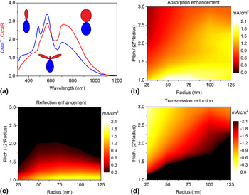
Figure 4(a) shows C scaT and C scaR for an r = 75 nm Ag nanoparticle in ITO sitting on the interface to glass (refractive index 1.5). Backwards scattering is strongly pronounced above a wavelength of 600 nm. The insets of the ADF of the scattered light also indicate the high backwards fraction and scattering into high angle modes. For the nanoparticle at the front interface of air to AZO, the forward scattering was prominent. Now at the rear interface with inverted refractive index conditions, despite illumination from the same direction, backwards scattering is significant. As dipole scattering happens preferentially to the layer with the highest refractive index, which in our solar cell structure is the absorber, light scattering is always beneficially oriented. This scattering directivity toward higher index media is the most beneficial effect of metallic nanoparticles for our application.
Theoretical integration of metallic Ag nanoparticles at back (ITO/glass) interface. (a) Scattering cross-section in forwards (C scaT, blue) and backwards (C scaR, red) direction for an r = 75 nm nanoparticle, insets show angular scattering distribution for wavelengths of 490, 570 and 710 nm; (b) absorption enhancement in CIGSe as function of radius and multiple, (c) corresponding reflection enhancement, and (d) transmission reduction of the solar cell.

Figure 4(b) plots the absorption enhancement of the CIGSe solar cell as a function of radius and pitch (multiple m of diameter) of the Ag nanoparticles inserted underneath ITO. Compared to the reference solar cell on a transparent ITO back contact but without nanoparticles, absorption is increased up to 2.2 mA/cm2 in the parameter range investigated and a maximum absolute value of 26.5 mA/cm2 reached (r = 50 nm, m = 1); note that radii above 150 nm would not be feasible underneath an ITO layer of 250 nm thickness considering volume compensation but no conformal overgrowth. (250 nm ITO were chosen since we will see later that a 50 nm passivating layer with similar refractive index will need to be added to the 200 nm ITO.) The increase in absorption can be correlated to an increase in reflection [Fig. 4(c)] and a reduction in transmission [Fig. 4(d)]. Maximum reflection and absorption enhancement combined with highest transmission reduction are observed for the maximum coverage of closely packed nanoparticles. Compared to a reference with a planar Ag back reflector underneath ITO, which can reach a maximum of 27.1 mA/cm2, these nanoparticle structures always provide less enhancement than the planar back reflector. On the other hand, they can provide transmission values coming close to the pure transparent back contact and which corresponds to 2.0 mA/cm2 absolute in the case of r = 50 nm, m = 1. The sum of absorption and transmission of the solar cell structures with nanoparticles can significantly surpass the bare absorption with a back reflector underneath ITO since reflection is reduced. The large angular distribution of the light scattered back from the nanoparticles is beneficial to a certain extent, although diminished again due to the interlayer. By adjusting the coverage, the nanoparticles offer the opportunity to carefully tune absorption and transparency of the device, making it adaptable for configurations like tandem solar cells or semitransparent solar cells. In the case of a single junction device, transmitted light can also be exploited using an additional back reflector at the rear interface to scatter light back into the structure.
b. Experimental
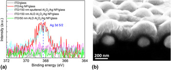
Looking at the experimental realization of Ag nanoparticles integrated underneath the transparent ITO back contact, thermal stability is the key challenge. To test whether diffusion is blocked, Ag nanoparticles of approx. 200 nm major diameter on a glass substrate (experimentally, the nanoparticles are more hemispherical and not symmetric) were overcoated with 200 nm ITO. The sample was then exposed to a CIGSe absorber growth process, thus experiencing the full high temperature run, but material deposition was avoided using a mask. The maximum process temperature was reduced from the standard 610 to 440 °C to minimize thermal impact. The process temperature cannot be reduced below 440 °C without compromising the device efficiency. Reference Yin, Brackmann, Hoffmann and Schmid17 Despite this temperature reduction, according to the XPS measurements presented in Fig. 5(a) (red curve), Ag is still found on the ITO surface after the process and diffusion could not be avoided.
Experimental integration of metallic Ag nanoparticles at back (ITO/glass) interface. (a) XPS measurements probing diffusion of Ag through ITO or ITO plus various passivating layers during a high temperature absorber deposition process; (b) SEM cross-section of thermally stabilized Ag nanoparticles underneath 50 nm ALD Al2O3 and 200 nm ITO. Reference Yin, Brackmann, Hoffmann and Schmid17

Since a further reduction of process temperature is not an option, an additional diffusion blocking layer was inserted between the nanoparticles and the ITO. Al2O3 was chosen due to a similar refractive index as ITO, low parasitic absorption, and known use as passivation layer. In the first attempt, 150 nm sputtered Al2O3 was used, but no passivation was found. Since atomic layer deposition (ALD) is known to form highly compact layers, next 150 nm of Al2O3 was deposited via ALD. In this case, the Ag diffusion could be blocked and no signal was detected via XPS. Due to the high material quality, the thickness of ALD Al2O3 could even be reduced to 50 nm while maintaining the thermal passivation of the Ag nanoparticles [compare the green curve in Fig. 5(a)].
Figure 5(b) shows the cross-sectional SEM image of the successful structure ITO/50 nm ALD Al2O3/Ag nanoparticles/glass. A further experimental challenge arises from the fact that the required high coverage with Ag nanoparticles makes the back contact mechanically fragile. Scribing of the absorber for separating individual solar cells can easily delaminate the ITO back contact which due to the nanoparticles has a low adhesion to the substrate. An experimental proof of absorption enhancement using Ag nanoparticles underneath the transparent back contact of an ultrathin CIGSe solar cell is therefore challenging. Enhanced absorption could be found in optical measurements, the electrical proof is still lacking. More details can be found in Ref. Reference Yin, Steigert, Andrae, Goebelt, Latzel, Manley, Lauermann, Christiansen and Schmid32.
In other technologies, in particular Si photovoltaics, the integration of Ag nanoparticles at the rear contact of the solar cell has been proven to be positive for absorption enhancement. The superstrate configuration in c-Si Reference Yang, Pillai, Mehrvarz, Kampwerth, Ho-Baillie and Green33 or the lower process temperatures for a-Si deposition than for CIGSe Reference Tan, Santbergen, Smets and Zeman34,Reference Ferry, Verschuuren, Li, Verhagen, Walters, Schropp, Atwater and Polman35 facilitate a stable integration of the Ag nanoparticles. Only a thin electrically passivating layer is required to separate the nanoparticles from the absorber layer. Thus, scattering, near-field enhancement and in the case of regular particle arrangements also coupling to waveguide modes can be exploited effectively. For CIGSe solar cells, electrically and thermally stable integration of nanoparticles underneath the absorber resulted in a relatively thick interlayer system. Therefore, after successful stabilization, effective coupling of light back to the absorber remains the central challenge.
B. Core-shell nanoparticles
1. Theoretical
In the previous section we have looked at Ag nanoparticles integrated at the rear of a CIGSe solar cell. Due to the challenge of Ag diffusion into the absorber material at high process temperatures, the nanoparticles were inserted underneath the ITO transparent back contact and even an additional Al2O3 passivating layer was required to thermally stabilize them. In contrast, a close contact to the absorber layer would make it possible to fully benefit from the large-angle scattering and the enhanced near-field of the nanoparticles. Therefore, thermally but also electrically well-passivated metallic nanoparticles directly integrated into the absorber layer would be advantageous. This leads us to the consideration of metal-dielectric core-shell nanoparticles.
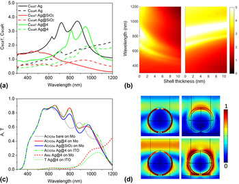
Figure 6(a) shows in black the scattering of an r = 75 nm nanoparticle in CIGSe and at the interface to Mo. The high-index surrounding has strongly red-shifted the resonances [compared to that of Fig. 4(a)], but the scattering cross-sections are equally high. Now we aim at maintaining the high scattering whilst electrically and thermally passivating the Ag nanoparticles in the absorber layer. Core-shell nanoparticles with a metal core and a dielectric shell are widely used for various applications. SiO2 is a very common shell material, thus we firstly assume a Ag@SiO2 nanoparticle with a shell thickness t = 10 nm. The resulting scattering cross-section is plotted in red in Fig. 6(a): resonances are blue-shifted and the maximum value has dropped from approximately 4 to less than 2. Integration of these nanoparticles does not appear promising due to the poor optical properties. The reason for the scattering reduction of the Ag@SiO2 nanoparticles can be seen in the low refractive index of the shell material as compared to the surrounding CIGSe. As explained in Ref. Reference Manley, Schmidt and Schmid36, the low index shell traps the light in its inside and outwards scattering and fields are strongly suppressed. The solution is to choose a medium with a high refractive index as shell material. Since CIGSe has a refractive index of approximately 3, we choose a constant refractive index of 4 for the shell material to exemplify this idea. The green curve in Fig. 6(a) shows the scattering of the Ag@n = 4 (Ag@4) nanoparticle, with the shell thickness kept at 10 nm. Resonances red-shift by approximately 100 nm compared to the bare nanoparticle, and scattering efficiency is only slightly reduced. These nanoparticles appear highly promising for direct integration and absorption enhancement in CIGSe.
Theoretical integration of core-shell nanoparticles at back (CIGSe/contact) interface. (a) Scattering cross-section in forward (C scaT) and backward (C scaR) direction for an r = 75 nm bare Ag nanoparticle, a Ag@SiO2 and a Ag@4 (10 nm shell thickness) core-shell nanoparticle in CIGSe to Mo; (b) C sca as a function of shell thickness and wavelength for SiO2 (left) and n = 4 shell (right) around the Ag nanoparticle in homogeneous CIGSe; (c) absorption in CIGSe for the Ag@SiO2 and the Ag@4 core-shell nanoparticles integrated in CIGSe to Mo and the Ag@4 particles in CIGSe to ITO as compared to the bare solar cell, absorption in Mo (A Mo), and transmission T are given for the case of Ag@4 nanoparticles on Mo and ITO, respectively; (d) electric field distribution for Ag@SiO2 (left column) and Ag@4 (right column) core-shell nanoparticles in the solar cell structure for λ = 800 nm (top row) and λ = 950 nm (bottom row).

To investigate the influence of shell thickness, Fig. 6(b) plots the scattering cross-sections of Ag@SiO2 (left) and Ag@4 (right) nanoparticles in a homogeneous CIGSe surrounding as a function of wavelength and shell thickness. For the Ag@SiO2 nanoparticles, scattering is essentially repressed when the shell thickness reaches 3 nm, whereas for Ag@4 nanoparticles, scattering is maintained up to approx. t = 10 nm. Since a 3 nm shell is not expected to provide any thermal passivation, this further supports the claim that a SiO2 shell will not be beneficial.
Next, we look at the results of integrating core-shell nanoparticles at the CIGSe/Mo interface of the complete solar cell structure. A minimum pitch was identified as ideal for the r = 75 nm Ag nanoparticles in a 10 nm shell of refractive index 4. In the following, we focus on a multiple of 1.25 times the diameter. Figure 6(c) compares the absorption in CIGSe for that case (red) to the absorption without nanoparticles (gray). An increase of 1.6 mA/cm2 short circuit current density is observed. For the same nanoparticles but with a SiO2 shell, the increase would only be 0.6 mA/cm2, see the blue curve. The peak positions with integrated nanoparticles are at the same wavelengths, because they are only related to the CIGSe film thickness which is changed for volume compensation. Yet, the enhancement is lower for the low-index shell in the entire wavelength range from 600 to 950 nm. As we have seen for the Ag nanoparticles underneath ITO, a transparent back contact allows for a reduction in Mo parasitic absorption and an excellent balance between absorption enhancement and transparency. Therefore, in Fig. 6(c) we further show the case of Ag@4 nanoparticles on an ITO back contact and present absorption in CIGSe and transmission of the device (green). (The ITO thickness was set to 250 nm for better comparability to Ag nanoparticles underneath the back contact.) Absorption enhancement corresponding to a short circuit current density of 1.9 mA/cm2 is even better than that for the situation on Mo back contact. In addition to that a transparency corresponding to 2.7 mA/cm2 can be exploited. The absorption losses in Mo (red-dashed curve), equal to 3.8 mA/cm2, mostly translated to transmission. This transmission can be exploited in a semitransparent device or be reflected back into the structure for further absorption enhancement.
Finally, in Fig. 6(d) we present the electric field distributions around the core-shell nanoparticles for the SiO2 shell (left) and the refractive index 4 shell (right) for λ = 800 nm (top) and λ = 950 nm (bottom) in the solar cell structure. It is clearly revealed how the low-index shell traps the light, whereas the high-index one promotes the field propagation. Reference Manley, Schmidt and Schmid36
b. Experimental
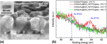
Similarly to the case of metallic nanoparticles integrated underneath an ITO back contact, also for the metal@dielectric core-shell particles thermal passivation has to be proven experimentally. Typically used core-shell nanoparticles are Au@SiO2, which are commonly accessible in the experiment. Therefore in contrast to the theoretical studies performed consistently for Ag, we chose Au as core material and SiO2 for the shell in the basic experimental studies of diffusion. Only if diffusion through thin shell materials can be handled at all, will it be worth to seek out more optically suitable shell materials. Figure 7(a) shows the SEM cross-section of the Au@SiO2 nanoparticles underneath an ultrathin CIGSe absorber layer. In the inset, a TEM view of the nanoparticles is presented. It clearly reveals the core-shell structure of the ellipsoidal nanoparticles with a maximum diameter of approx. 50 nm.
Experimental integration of core-shell nanoparticles at back (CIGSe/contact) interface. (a) Au@SiO2 core-shell nanoparticles underneath a CIGSe absorber layer, inset shows TEM of bare core-shell nanoparticle; (b) XPS measurement probing diffusion of Au through SiO2 shell for various process temperatures of CIGSe deposition.

The visual presence of the nanoparticles under the absorber is already a good indication for their preservation. To investigate diffusion of the metal into and through the absorber layer, again XPS measurements were performed. Figure 7(b) summarizes the results: Whereas for the high process temperature of 610 °C, Au is observed on top of the CIGSe layer; for lower temperatures of 440 and still 510 °C, Au does not diffuse through the absorber. In these cases the particles can be assumed stable. For the experimental realization of the theoretically predicted promising structures, core-shell nanoparticles like Ag@AlSb would be desirable. These however pose the next challenge since the fabrication of a high refractive index dielectric shell is not a commonly established method. An alternative approach might consist in forming the shell from amorphous Si as it is a very commonly used semiconductor offering a high refractive index and a good transparency at least above its band gap of 1.7 eV. Judging from the highly promising properties of metal nanoparticles with a high refractive index shell and the potential of broader application, further research may be desirable.
Therefore, also for the optically effective integration of core-shell nanoparticles, CIGSe solar cells pose severe challenges. The beneficial integration of Au@SiO2 (Ref. Reference Chen, Zhang, Zhou, Huang, Zhao, Wang, Liu, Lu and Yang37) and Au@PVP Reference Xu, Liu, Meng and Huang38 nanoparticles has been proven in low refractive index organic or dye sensitized solar cells, respectively. In the case of successful application of metal-insulator core-shell nanoparticles in the high refractive index perovskite absorber layer, effects beyond pure optical benefits are claimed to be the reason for enhancement. Reference Saliba, Zhang, Burlakov, Stranks, Sun, Ball, Johnston, Goriely, Wiesner and Snaith39 From the optical point of view we thus underline the need of high refractive index shell material to effectively exploit optical effects from core-shell nanoparticles in CIGSe solar cells.
C. Dielectric nanoparticles
1. Integration at front
a. Theoretical
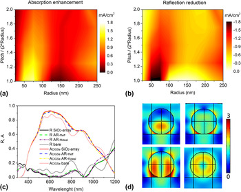
Plasmonic metal nanoparticles revealed two fundamental drawbacks: parasitic absorption and low thermal stability. To avoid these negative influences, we turn instead to photonic nanoparticles made from dielectrics. They can provide scattering cross-sections equally high as metallic nanoparticles Reference Schmid, Andrae and Manley40,Reference Akimov, Koh, Sian and Ren41 due to the presence of resonant modes. As the dielectric nanoparticles are free from parasitic absorption, we can easily place them on top of the finished solar cell to exploit their light coupling behavior. In Fig. 8(a) the absorption enhancement resulting from SiO2 sphere arrays is mapped for various nanoparticle radii and pitches. Closely packed arrays (m = 1) are the most beneficial with a trend toward slightly increased spacing (m = 1.25) for larger radii. Two distinct maxima can be observed: one for smaller radii of 60–75 nm, the other one for radii of 250 nm and above. These two cases will be discussed in the following.
Theoretical integration of dielectric SiO2 nanoparticles at front (air/AZO) interface. (a) Absorption enhancement in CIGSe as function of radius and multiple and (b) corresponding reflection reduction; (c) reflection R and absorption in CIGSe A CIGSe for antireflection coatings of r = 75 nm closely packed SiO2 nanospheres (SiO2-array), a d = 150 nm and n eff = 1.24 layer (AR-n eff) and a d = 138 nm and n ideal = 1.35 layer (AR-n ideal) as compared to the bare cell; (d) electric field distributions around r = 250 nm spheres for wavelengths 610 nm (top left), 640 nm (top right), 670 nm (bottom left) and 700 nm (bottom right).

For the smaller spheres, the peak in absorption enhancement corresponding to 1.6 mA/cm2 comes with a clear reduction in reflection, compare Fig. 8(b). Actually, these particles are too small to show Mie resonances in the visible wavelength range which would lead to strong light interaction. For comparable resonance wavelengths, the dielectric nanoparticles generally need to be significantly larger than the metallic ones, see also Ref. Reference Schmid, Andrae and Manley40. Therefore, the origin of the pronounced reduction in reflection cannot lie in resonant behavior. The closely packed nanoparticle array of r = 75 nm SiO2 spheres with refractive index n = 1.46 surrounded by air has an effective refractive index n eff = 1.24. The thickness of this effective index layer is d eff = 150 nm, which fulfills the λ/(4n) condition for λ = 744 nm. n eff is close to the ideal value n ideal = (n 1 × n 2)1/2 = 1.35 for the refractive index of the intermediate antireflection layer between air (n 1 = 1) and AZO (n 2 = 1.82 @ 744 nm). The ideal thickness in this case would be d ideal = 138 nm, which is also very comparable to the effective thickness of nanospheres in air. Figure 8(c) compares the reflection of the ultrathin CIGSe solar cells with the 75 nm radius SiO2 sphere array on top (black line) to the one with the effective (green dashed) and the one with the ideal (purple dash-dotted) antireflection layer. They are very similar and all show a strong reduction in comparison to the cell without an antireflection coating (gray reference line). As the “ideal” antireflection layer was calculated for the interface air/AZO only, the nanosphere antireflection layer can reduce the reflection even more and another advantage lies in its increased acceptance angle. Whereas for planar layers, reflection can increase drastically with nonperpendicular incidence, the nanospheres take in light equally well from a wide angular range and for certain cases reveal even more pronounced field enhancements than for normal incidence. Reference Grandidier, Weitekamp, Deceglie, Callahan, Battaglia, Bukowsky, Ballif, Grubbs and Atwater10 The reduction in reflection directly translates to an increase in absorption as the curves in Fig. 8(c) show.
Moving on to the larger spheres, the increase in absorption is not as pronounced, but becomes significant for spheres above 200 nm radius [Fig. 8(a)]. Here, Mie resonance can again be observed for visible wavelengths. Due to the large particle size a multitude of modes occurs and since we are dealing with dielectrics, electric and magnetic modes are equally strongly pronounced. Reference Schmid, Andrae and Manley40,Reference van de Groep and Polman42 The Mie resonances of the dielectric nanoparticles always reveal a strong forward scattering or even focusing behavior. Reference Schmid and Manley43 This effect can be seen in the electric field representation of the r = 250 nm nanospheres on top of the solar cell structure (excerpt of nanoparticles in air on AZO shown) for the wavelengths 610, 640, and 670 nm [Fig. 8(d) top left, top right and bottom left]. A strong transition between different modes even within this short wavelength interval is observed. At λ = 700 nm, still another mode occurs which can be deduced to be a whispering gallery mode based on the field pattern [Fig. 8(d) bottom right]. Reference Oraevsky44 High electric field intensities following the inner surface of the nanosphere are revealed. Thus, the large dielectric nanoparticles have a strong light interaction and the various modes can help to improve the performance of an underlying solar cell. Similar to the metallic nanoparticles, losses and incomplete light penetration down to the absorber layer need to be considered here as well. Therefore, as a conclusion for dielectric nanoparticles at the front interface, the antireflection effect of the small dielectric nanospheres can be seen as the most beneficial.
b. Experimental
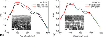
Figure 9 presents the experimental results of depositing dielectric nanoparticles at the front interface of ultrathin CIGSe solar cells. Measurements of quantum efficiencies are given, while the insets show SEM images of the closely packed SiO2 spheres on top of the solar cell. In Fig. 9(a) the case of small spheres with 60 nm radius is represented. A clear increase in quantum efficiency over almost the entire wavelength range is observed. This almost wavelength-independent behavior and the smoothening of interference fringes are in good agreement with the theoretically predicted antireflection effect. A total increase in short circuit current density of 2.1 mA/cm2 was measured for this device with 460 nm absorber thickness.
Experimental integration of dielectric SiO2 nanoparticles at front (air/AZO) interface. EQE of ultrathin CIGSe solar cell with SiO2 nanoparticles on top for (a) r = 60 nm and (b) r = 300 nm spheres as compared to the bare solar cell; insets show SEM cross-sections of the devices. Reference Yin, Manley and Schmid45

The case of larger nanospheres was experimentally realized using r = 300 nm particles and is shown in Fig. 9(b). Around 500–600 and 900 nm wavelength a small increase is observed. As we have seen from the theoretical investigations, the various order Mie resonances and whispering gallery modes of the large nanospheres only occur in narrow wavelength bands. Since experimentally the perfect conditions of nanoparticle packing cannot be guaranteed, particularly the modes which rely on the nanoparticle interaction are hard to reveal. A larger benefit therefore clearly results from the small antireflection sphere arrays. Detailed experiments can also be found in Ref. Reference Yin, Manley and Schmid45.
Benefits of dielectric nanosphere coatings have been revealed e.g., in GaAs and Si solar cells. Whispering gallery modes, Reference Grandidier, Weitekamp, Deceglie, Callahan, Battaglia, Bukowsky, Ballif, Grubbs and Atwater10 mixed graded index Mie-scattering Reference Lin, Zhong and Fu46 and focusing behavior Reference Simovski, Shalin, Voroshilov and Belov47 of nanoparticles have been identified to lead to enhanced incoupling of light. All these examples benefit from a close distance of the nanospheres to the absorber layer. Again, CIGSe solar cells with thicker front layers consisting of AZO, i-ZnO, and CdS complicate coupling of light from resonant modes into the absorber. The increased spacing effectively makes only the antireflection behavior beneficial.
2. Integration at back
a. Theoretical
Placing the nanoparticles in close vicinity to the absorber layer has been identified as advantageous for enhancing the absorption in CIGSe and not in the contact layers. For the metallic nanoparticles this close contact to the absorber was complicated by diffusion of the nanoparticle material. Recombination of charge carriers at the metal surfaces was another drawback. Using metal nanoparticles wrapped in a dielectric shell was an option to overcome these challenges and still exploit the plasmonic enhancement properties. On the other hand, we can directly consider pure dielectric nanoparticles and exploit their photonic resonances. Due to the high thermal and electrical stability dielectric particles can be directly integrated underneath the absorber layer.
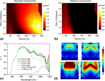
Figure 10(a) shows the absorption enhancement for SiO2 nanoparticles integrated at the CIGSe/Mo interface as a function of nanoparticle radius and pitch in multiple m of diameter. Small spheres have a negligible effect, only starting from a radius of approximately 100 nm is absorption enhancement observed. The case of r = 250 nm and m > 1.5 is represented in black in the figure since these parameter settings could not be calculated for an absorber layer of 400 nm thickness and considering volume compensation but not conformal overgrowth of CIGSe. A maximum enhancement of 3.6 mA/cm2 is found for r = 225 nm and m = 1.25 which corresponds to a total of 29.1 mA/cm2 short circuit current density. Compared to the integration of Ag nanoparticles underneath ITO or core-shell nanoparticles on Mo, the enhancement is more than two times higher. Also the enhancement obtained by integrating dielectric nanoparticles at the front interface is significantly surpassed. In that latter case, the smaller nanoparticles performed best, acting as an effective antireflection coating. For the case of dielectric nanoparticles at the rear interface, reflection is enhanced for the small nanoparticles [see Fig. 10(b)], corresponding to a beneficial backscattering toward the absorber. In the range of highest absorption enhancement, reflection is however reduced, underlining the strong light trapping.
Theoretical integration of dielectric SiO2 nanoparticles at back (CIGSe/Mo) interface. (a) Absorption enhancement in CIGSe as a function of radius r and pitch over diameter (multiple m) and (b) corresponding reflection enhancement on the same scale; (c) absorption in CIGSe as a function of wavelength for the case of m = 1.25 and radii 200, 225, and 250 nm spheres compared to the bare solar cell, also shown the case of r = 225 nm spheres on ITO and (d) electric field distributions around the spheres for r and λ equal to top left: 200 and 1090 nm, top right: 225 and 1100 nm, bottom left: 225 and 1180 nm and bottom right: 250 and 1160 nm.

For the most promising multiple m = 1.25, Fig. 10(c) depicts the wavelength dependent absorption in CIGSe for the three largest radii investigated (200, 225, and 250 nm). A strong enhancement in the entire wavelength range above 530 nm is observed as compared to the reference without integrated nanoparticles (gray). The case of a transparent back contact (250 nm ITO as previously) is depicted as well for the optimum r = 225 nm particles and in addition to an absorption enhancement of 3.6 mA/cm2 a transmission corresponding to 3.1 mA/cm2 can be gained here. In the absorption curves for integrated nanoparticles Fabry–Perot resonance peaks red-shift related to the compensated height of the CIGSe layer. On top of these peaks, at long wavelengths strongly pronounced resonances appear. Whereas the broadband enhancement above 530 nm can be linked to Mie resonances, the distinct peaks visible above 1100 nm are attributed to waveguide modes which result from the nanoparticle coupling. Reference Yin, Knight, van Lare, Polman and Schmid48 Figure 10(d) reveals the electric field distributions at the peak positions. For the smallest shown particle (r = 200 nm), the field enhancement on a scale from 0 to 3 is still weak, see the top left picture. For the r = 225 nm particle, the same mode (bottom left picture) leads to a huge field localization in the absorber, explaining the strong resonance peak at λ = 1180 nm. For the same sphere, another resonance appears at λ = 1100 nm which is shown in the top right picture. This mode is the prominent one for the r = 250 nm sphere and becomes much more pronounced here as shown in the bottom right picture. The field localization either on top or at the side edges of the spheres is generally observed also for other shapes of dielectric nanoparticles integrated at the rear interface of an ultrathin CIGSe solar cell. For more details and the distribution of field intensities in case of hemispherical or tapered structures see Ref. Reference Yin, Knight, van Lare, Polman and Schmid48.
b. Experimental
A spacing of approximately half the diameter of the dielectric spheres integrated at the rear interface has been shown to be the theoretical optimum. In contrast to the front interface, a closely packed sphere array would also not be electrically beneficial here since the rear contact would be isolated. Increasing the spacing between the spheres is thus crucial from an optical and an electrical point of view. Experimentally, the size of the PS spheres can easily be reduced by plasma etching in oxygen atmosphere. Yet, the PS spheres are not thermally stable and would not persist at the rear interface after the high temperature deposition process of CIGSe. SiO2 spheres therefore would be preferred, but in this case plasma etching generates greenhouse gasses making handling more complicated.
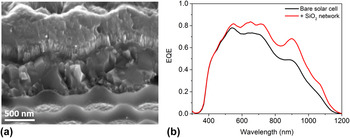
One solution is an alternative fabrication of the SiO2 nanoparticles, e.g., by nanoimprinting. For nanoimprinted dielectric patterns at the Mo/CIGSe interface, we have shown an increase in short-circuit current density of 2.3 mA/cm2 and a related efficiency of 12.3% for ultrathin absorbers. Reference van Lare, Yin, Polman and Schmid49 But also the approach of nanosphere lithography offers an alternative option for fabrication of thermally stable dielectric nanostructures: the etched PS sphere template can serve as a mask for SiO2 deposition and after removal of the PS spheres a SiO2 network remains. The resulting network is depicted in Fig. 11(a)—free standing on Mo in the front and overcoated with the CIGSe solar cell at the back. For this example, PS spheres with a diameter of 909 nm, which could be reduced to 630–640 nm by plasma etching for 12 min in O2 at a pressure of 0.2 mbar, were used as a mask for SiO2 deposition.
Experimental integration of dielectric SiO2 nanopatterns at back (CIGSe/Mo) interface. (a) Cross-sectional SEM picture of ultrathin CIGSe solar cell with SiO2 network at the back contact (visible free-standing on Mo in the front); (b) broadband EQE enhancement by integration of the network.

Figure 11(b) provides evidence for the benefits of integrating the SiO2 network at the rear of an ultrathin CIGSe solar cell. As can be seen from the quantum efficiency measurement, the absorption is significantly enhanced in the entire wavelength range from 500 to 1200 nm. A related increase in short circuit current density from 23.8 to 27.7 mA/cm2 leads to a relative increase in efficiency by 14%. Compared to the theoretical predictions for the integration of SiO2 nanoparticles, the network does not exhibit sharp resonances above 1100 nm which can be related to different resonance conditions for particles and holes. However, the network configuration may provide an additional benefit over the particles: since a much larger back contact area is covered with isolating SiO2, point contacts are formed which can reduce rear surface recombination. Reference Vermang, Wätjen, Fjällström, Rostvall, Edoff, Gunnarsson, Pilch, Helmersson, Kotipalli, Henry and Flandre50 Thus the structure is able to combine electrical and optical benefits.
Again, absorption enhancement by integration of dielectric nanoparticles at the rear interface has first been proven for Si solar cells. Dielectric nanoparticles acting as Mie scatterers Reference van Lare, Lenzmann and Polman9 or diffractive elements Reference Wang, Mokkapati, White, Soderstrom, Varlamov and Catchpole51 were reported. Since in the case of thermally and electrically stable dielectric nanoparticles we can also achieve direct integration underneath CIGSe, this is the most promising configuration for chalcopyrite-based solar cells. We could successfully prove significant absorption enhancement Reference van Lare, Yin, Polman and Schmid49 and additionally identify electrical benefits of the nanostructures at the back contact. Reference Yin, Knight, van Lare, Polman and Schmid48
IV. SUMMARY
In this paper, we have investigated metallic, metal-dielectric core-shell, and dielectric nanoparticles integrated either at the front or the rear interfaces of an ultrathin CIGSe solar cell. The example calculations were assuming spherical nanoparticles which may not necessarily correspond to the realistic situation. Therefore, absolute values of absorption enhancement for the various configurations given here should be used for comparative purpose only and final enhancement benchmarked against maximum expected values for the respective experimental geometries. In the following, we summarize the major benefits and drawbacks of the different configurations.
Ag nanoparticles at the front air/AZO interface provide a strong forward scattering which can be theoretically exploited to reduce reflection of the device. Yet, the metallic nanoparticles also show parasitic absorption which is strongly pronounced for small particles and can be mostly suppressed for radii larger than 75 nm. The scattering into a large angular range is another characteristic of the metallic nanoparticles, which is however attenuated due to the front contact layers separating the nanoparticles from the absorber. Losses in contact layers are a general drawback when nanoparticles are not directly touching the absorber. The maximum theoretical enhancement found was 1.2 mA/cm2. Experimentally, particle integration at the front avoids interfering with device processes. In the case of metallic nanoparticles, annealing steps have to be considered carefully due to the temperature impact on the device. It is found that in the experiment Ag nanoparticles on top of CIGSe solar cells generally increase the reflection rather than reduce it.
Ag nanoparticles at the rear (ITO/glass) interface are a promising alternative to suppress parasitic absorption in the first place and exploit backscattering of the metallic nanoparticles toward the high index absorber layer. Since thermally and electrically passivating layers are required between the nanoparticles and the absorber, there is only a limited exploitation of scattering and near-field effects and losses in contacts need to be accepted. Integration in a device with a transparent back contact is also beneficial from the perspective of reduced absorption in Mo. The maximum theoretical enhancement found was 2.2 mA/cm2 plus 2.0 mA/cm2 transmission. Experimentally, a thermal passivation of Ag nanoparticles can be achieved by ALD Al2O3. Remaining challenges lie in the mechanically stable contact formation with integrated nanoparticles.
Ag@dielectric core-shell nanoparticles can be directly integrated underneath the absorber layer. A high refractive index shell material is required to avoid trapping light in the shell. In the case of a refractive index equal to or higher than the surrounding, a shell thickness of 10 nm, which is expected to provide passivation, is acceptable. Scattering and near-fields are then directly exploited in the absorber layer. In the case of a transparent back contact, absorption enhancement and transmission can be flexibly balanced using the nanoparticles. The maximum theoretical enhancement found was 1.9 mA/cm2 plus 2.7 mA/cm2 transmission. Experimentally, thermal stabilization can be achieved for metal-dielectric core-shell nanoparticles underneath the absorber layer. The challenge lies in fabricating adequately sized (radii larger 75 nm) core-shell particles with a high refractive index shell material.
SiO2 nanoparticles at the front (air/AZO) interface are able to enhance light incoupling without parasitic absorption in the nanoparticles. The antireflection effect of the small nanospheres (radii around 75 nm) is most pronounced and can outperform a planar antireflection layer in terms of increased acceptance angle of incident light. For larger spheres (e.g., 225 nm radius) Mie resonances and whispering gallery modes dominate, which show a spectrally confined and thus weaker overall enhancement. Losses in the contact layers need to be considered here as well. The maximum theoretical enhancement found was 1.6 mA/cm2. Experimentally, the deposition of dielectric particles on top of the finished solar cell is straight forward and the related chemical processes are compatible with CIGSe solar cells. Enhancement in line with the theoretical predictions could be demonstrated.
SiO2 nanoparticles at the rear (CIGSe/Mo) interface provide the strongest light interaction and resonances leading to efficient light trapping. The direct contact to the absorber layer, feasible for these electrically and thermally passivated nanoparticles, proves to be highly beneficial. The light collected by the nanoparticles can be directly coupled to the absorber layer. The structures also benefit from a regular arrangement of the nanoparticles with close spacing and thus nanoparticle coupling. The maximum theoretical enhancement found was 3.6 mA/cm2 and in the case of a transparent back contact, an additional 3.1 mA/cm2 transmission. Experimentally, the dielectric nanostructures can be successfully integrated in the solar cell and a conformal overgrowth with the absorber layer achieved. 3.9 mA/cm2 enhancement in short circuit current density for a dielectric network on Mo is shown in this paper.
Compared to other solar cell technologies (e.g., Si, GaAs, or organic absorber materials), CIGSe solar cells pose particular challenges for the effective integration of nanostructures for absorption enhancement. The high temperature absorber deposition process requires not just electrical but also thermal passivation for rear interface integration. Much thicker contact and additional passivation layers complicate placing the nanoparticles in close vicinity to the absorber, which however is of utmost importance for effective enhancement. Therefore, directly integrated, stable dielectric nanoparticles have proven most beneficial and gave the best improvement.
Looking beyond just optical enhancement, dielectric nanostructures have also been identified to provide back surface passivation. Point contact structures have been proposed in Ref. Reference Vermang, Wätjen, Fjällström, Rostvall, Edoff, Gunnarsson, Pilch, Helmersson, Kotipalli, Henry and Flandre50 and the combined optical and electrical benefit of dielectric nanoparticles was just recently proven in Ref. Reference Yin, Knight, van Lare, Polman and Schmid48. Transparent back contacts are the key to most efficient light exploitation and the nanoparticles allow for a wavelength dependent balance between absorption and transmission which is of high interest for semitransparent devices.
In total, metallic nanoparticles are beneficial for their scattering toward high-index materials and into large angles, but suffer from parasitic absorption and lack of electrical and thermal passivation. Metal-dielectric core-shell nanoparticles can be a way to confront the passivation challenge and provide efficient enhancement when integrated into the absorber. Generally, any separation layer between nanostructures and absorber should be avoided to minimize losses. Dielectric nanoparticles have proven to be most beneficial, due to their high stability and strong resonant modes. Furthermore, they enable a combined optical-electrical benefit, which will be a focus of future investigations.
ACKNOWLEDGMENTS
The authors would like to thank S. Duan for absorber and C. Ferber & M. Kirsch for front contact fabrication, K. Harbauer for deposition of sputtered and M. Latzel & M. Goebelt for ALD Al2O3. A. Steigert is greatly acknowledged for performing XPS measurements. The work received funding from the Helmholtz Association for the Young Investigator Group VH-NG-928 within the Initiative and Networking Fund.