I. INTRODUCTION
Quantum technologies have the potential to play a key role in a wide variety of applications for the next generation of beyond Si-based technologies. One example is quantum computing which is being intensively developed not only by research institutes but also commercial companies such as IBM and Google1,Reference Boixo, Isakov, Smelyanskiy, Babbush, Ding, Jiang, Bremner, Martinis and Neven2 due to an expected increase in processing capacity beyond existing technology. In addition, there are applications such as quantum communication and quantum sensors which promise to secure networks and new diagnostics toward such as biology. Quantum manipulations of spins, initialization, preservation, operation, and readout are indispensable techniques to actualize quantum-based applications. For proof-of-concept experiments, single photon source (SPS) such as laser trapped ions,Reference Olmschenk, Younge, Moehring, Matsukevich, Maunz and Monroe3 rare-earth ions embedded in a crystal,Reference Ichimura4 quantum dots,Reference Petta, Johnson, Taylor, Laird, Yacoby, Lukin, Marcus, Hanson and Gossard5 and color centers in solids, e.g., negatively charged nitrogen-vacancy (NV) center in diamondReference Balasubramanian, Chan, Kolesov, Al-Hmoud, Tisler, Shin, Kim, Wojcik, Hemmer, Krueger, Hanke, Leitenstorfer, Bratschitsch, Jelezko and Wrachtrup6 have been utilized. Among them, solid-state SPS are advantageous due to easy integration within existing industrial process flows.
The NV center is an especially promising candidate for use as a quantum bit (qubit). The quantum state of the electron spins in a NV center is sensitive to its surrounding environments, and its quantum manipulations can be performed at room temperature. As a result, the NV center has great potential to be a nanoscale quantum sensor with high sensitivity, as well as, high spatial resolution for biological and medical applications. To date, quantum error correction,Reference Waldherr, Wang, Zaiser, Jamali, Schulte-Herbrüggen, Abe, Ohshima, Isoya, Du, Neumann and Wrachtrup7 detection of electric- and magnetic-fieldReference Balasubramanian, Chan, Kolesov, Al-Hmoud, Tisler, Shin, Kim, Wojcik, Hemmer, Krueger, Hanke, Leitenstorfer, Bratschitsch, Jelezko and Wrachtrup6,Reference Dolde, Fedder, Doherty, Nöbauer, Rempp, Balasubramanian, Wolf, Reinhard, Hollenberg, Jelezko and Wrachtrup8 and current flowReference Tetienne, Dontschuk, Broadway, Stacey, Simpson and Hollenberg9 have all been demonstrated.
In recent years, silicon carbide (SiC) has gathered much attention because its specific centers such as silicon vacancy (VSi),Reference Fuchs, Stender, Trupke, Simin, Pflaum, Dyakonov and Astakhov10,Reference Widmann, Lee, Rendler, Son, Fedder, Paik, Yang, Zhao, Yang, Booker, Denisenko, Jamali, Momenzadeh, Gerhardt, Ohshima, Gali, Janzén and Wrachtrup11 carbon antisite–vacancy pair (CSi–VC),Reference Castelletto, Johnson, Ivády, Stavrias, Umeda, Gali and Ohshima12 divacancy (VC–VSi),Reference Christle, Falk, Andrich, Klimov, Ul Hassan, Son, Janzén, Ohshima and Awschalom13,Reference de las Casas, Christle, Hassan, Ohshima, Son and Awschalom14 and SiO2/SiC interface defectsReference Lohrmann, Iwamoto, Bodrog, Castelletto, Ohshima, Karle, Gali, Prawer, McCallum and Johnson15–Reference Abe, Umeda, Okamoto, Kosugi, Harada, Haruyama, Kada, Hanaizumi, Onoda and Ohshima17 have been proved to act as SPS. Among them, VSi, with photoluminescent emission in the near infrared region,Reference Baranov, Bundakova and Soltamova18 is preferred for quantum sensors aiming for biological or medical applications working at ambient conditions. Nanoscale rf-drivenReference Simin, Soltamov, Poshakinskiy, Anisimov, Babunts, Tolmachev, Mokhov, Trupke, Tarasenko, Sperlich, Baranov, Dyakonov and Astakhov19,Reference Niethammer, Widmann, Lee, Stenberg, Kordina, Ohshima, Son, Janzén and Wrachtrup20 or rf-freeReference Cochrane, Blacksberg, Anders and Lenahan21 magnetometers and thermometerReference Anisimov, Simin, Soltamov, Lebedev, Baranov, Astakhov and Dyakonov22 have also been demonstrated using VSi.
SiC is well known as a promising material for high-power and high temperature-resistance devices because of superior physical properties such as wide band gap and high breakdown electric field. Unlike diamond, intensive development for more than a decade has given rise to commercially available high-quality and wafer-scale (up to 150 mm) substrates and sophisticated device fabrication processes (growth, doping, etc.), which is accelerating the practical use of SiC devices.
Diagnostics for such devices are become increasingly important from design to product. Si-based power devices equipped with various functional circuits (overcurrent and overheat protection, etc.) have been already commercialized. There are other practical techniques to detect the device state such as optical beam induced resistance change (OBIRCH) and various scanning probe microscopies. These have disadvantages, such as, macroscopic detection for circuits, failure analyses (a running device is a nontarget) for OBIRCH, and surface-only sensitivity for various microscopies. From the viewpoint of diagnostics, microscopic detection of the internal state of the device, such as electric-, magnetic-field, and the temperature, of a “running” device is the most accurate. For these reasons, SiC devices internally equipped with an SPS-based quantum sensor where the internal state can be detected by using emitted photons from SPS are a value-added product. Electrically controllable SPSs are useful elements for sensing running devices as the current needed to operate the device can also be used for exciting the SPSs. To combine a functional SiC device and a SPS based on VSi defect, it is important to establish a defect creation technique with both position and density (from single to ensemble) controllability. Crystal growth is superior in terms of the creation of color centers with less degradation to the base crystal. However, it is difficult to control the position and the density. Particle irradiation is a promising method to satisfy such controllability. A previous study introduced VSi into the light-emitting diode structure by electron irradiation to investigate the characteristics of electrically driven VSi.Reference Fuchs, Soltamov, Väth, Baranov, Mokhov, Astakhov and Dyakonov23 However, the conventional irradiation method is not able to irradiate particles into a desired area without specific processes such as implantation masks.
Proton beam writing (PBW), a direct lithographic particle irradiation method, is an effective technique to control the position and the density of the color centers. Using this method, it is possible to create irradiation defects at the desired location. The proton (H+) beam used in this study can be focused as small as 1 μm in diameter and with a position resolution of 15 nm. This is sufficient for SiC devices that are μm-size in dimension as needed to manage large electric power. It has been previously reported that PBW can create position-controlled optically excitable VSi without photolithography.Reference Kraus, Simin, Kasper, Suda, Kawabata, Kada, Honda, Hijikata, Ohshima, Dyakonov and Astakhov24,Reference Ohshima, Honda, Onoda, Makino, Haruyama, Kamiya, Satoh, Hijikata, Kada, Hanaizumi, Lohrmann, Klein, Johnson, McCallum, Castelletto, Gibson, Kraus, Dyakonov and Astakhov25 While it is difficult to avoid crystalline damage by particle irradiation including PBW, the effect of crystalline damage on optical properties of VSi has not yet been identified.
In this study, we introduced VSi into the SiC pn junction diode using PBW to investigate the optical properties of VSi, including comparison of the dependence of the electroluminescence (EL) and photoluminescence (PL) intensities on H+ fluence, and the effect of crystalline damage on the optical properties of VSi.
II. EXPERIMENTAL SECTION
A. Sample preparation
1. Fabrication of the pn junction diode
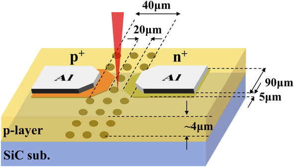
In-plane pn junction diodes fabricated by photolithography and ion implantation processes were used in this study. A sample structure is schematically shown in Fig. 1. A p-type epitaxial 4H-SiC layer with a thickness of 5.6 μm and a doping concentration of 1.5 × 1016 cm−3 grown on a 4H-SiC substrate (n-type, 4° off, Si-face) by AIST was utilized as a starting material. The p+- and n+-type regions were independently formed by aluminum (acceleration energy of 50, 75, and 110 keV, concentration of 2 × 1020 cm−3) and phosphorus (acceleration energy of 80, 140, and 200 keV, concentration of 5 × 1019 cm−3) ion implantations, respectively, at 800 °C, using a photo-resist and SiO2 stacked mask. The sample was subsequently annealed at 1800 °C for 5 min in Ar atmosphere for dopant activation. Finally, an Al electrode was deposited onto the p+- and n+-type regions by a lift-off process.
A sample structure of VSi embedded within an in-plane pn junction diode. VSi was introduced on the vicinity of the n+-type region and p-layer junction by PBW. Its depth was estimated to be 4 μm from the sample surface by SRIM simulations.

2. Creation of VSi acting as SPS
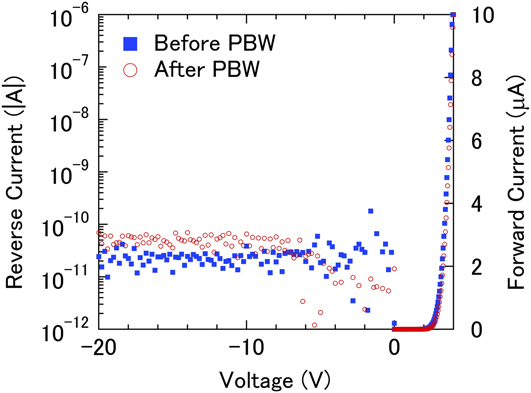
The VSi was introduced in the pn diode by PBW. A 0.5 MeV focused H+ beam was irradiated in the vicinity of the n+-type region and p-layer junction as shown in Fig. 1. The pattern used for PBW consists of three rows of 11 dots on a 10 μm pitch. Each row was also separated by 10 μm. The fluence was varied from 3 × 10⁴ to 3 × 10⁷ H+/dot by changing the dwell time. The defect depth was estimated to be ∼4 μm from the sample surface using SRIM simulations.26 No pre- and post-irradiation treatment was performed. It is noted that no significant difference in the current–voltage (I–V) characteristics was observed after the PBW process even at the highest fluence of 3 × 10⁷ H+/dot (Fig. 2).
I–V characteristics measured before and after PBW with 3 × 10⁷ H+ of fluence. No significant change was observed.

B. Electrical and optical characterization
EL and PL measurements were conducted using a home-built confocal microscope (CFM). Details about the CFM can be found in Ref. Reference Kato, Wolfer, Schreyvogel, Kunzer, Sebert, Obloh, Yamasaki and Nebel27. The sample was forward biased to obtain EL spectra and the confocal fluorescence mapping under constant current conditions of either 200 or 500 μA. The device was biased from 5 to 8 V, which showed essentially no H+ fluence dependence. For PL measurements, a cw laser was illuminated on a dot to excite the VSi without bias. Laser power was varied between 0.1 and 2 mW range. The long-pass filter (LPF) and laser wavelength were carefully selected as VSi shows fluorescence emission in the region of 800–1000 nm.Reference Baranov, Bundakova and Soltamova18 All measurements were performed at room temperature.
III. RESULTS AND DISCUSSION
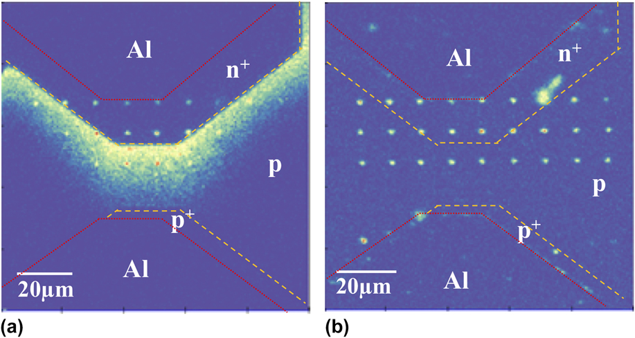
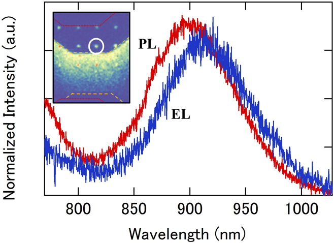
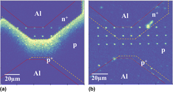
Fluorescence mappings of EL (I = 500 μA) and PL (P = 1 mW) recorded on the same sample with 1 × 10⁷ H+/dot fluence are shown in Figs. 3(a) and 3(b), respectively. An array of luminescent spots was clearly detected in both mappings. In EL and PL spectra taken from the same dot with 3 × 10⁵ H+ fluence as shown in Fig. 4, the emission peak with the same shape for both cases was observed between 800 and 1000 nm. As the peak was in accordance with previously reported results,Reference Baranov, Bundakova and Soltamova18 we conclude that VSis were created by PBW. These results suggest that VSi can be excited by photons as well as injected current (electrons and/or holes). It should be mentioned that no VSi-related EL and PL peaks were confirmed from the unirradiated areas. A pronounced luminescence was observed along the p–n+ junction for EL, which was assigned as emission from D1 defects.Reference Patrick and Choyke28 The distribution of luminescence was presumably associated with the geometry of p+- and n+-type layers and electrodes.Reference Lohrmann, Pezzagna, Dobrinets, Spinicelli, Jacques, Roch, Meijer and Zaitsev29
Fluorescence mappings of (a) EL (I = 500 μA) and (b) PL (P = 1 mW) recorded on the same sample with 1 × 10⁷ H+ of fluence. Bright spots were clearly observed at the irradiated area for both images. A 808 nm LPF (for EL and PL) and a 671 nm laser (for PL) were used. The dotted and broken lines represent boundary of n+- or p-type region/electrode and n+- or p-type region/p-type layer, respectively.

EL and PL spectra taken from the same dot marked with the white circle in the inset. Similar shape of the spectra indicates that emission originated from the same type defect (VSi). A 594 nm LPF (for EL and PL) and a 532 nm laser (for PL) were selected.

Difference of intensity depending on position (n+-, p-type regions) was observed in the case of EL. No emission was confirmed on lower left and right of the dot patterns. Since the intensity is related to an amount of current injected into VSi, the difference may reflect the distribution of current density. This suggests a possibility of current distribution imaging in the device using intensity of luminescence from VSi. Further studies are needed to confirm the point. In comparison, PL showed uniform intensity across the array because all VSis were equally excited by photons.
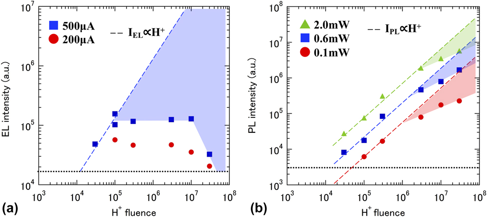
The dependence of the EL and PL intensities from VSi on H+ fluence were investigated to reveal if there is a difference of emission efficiency between electrical and optical excitation.
Figure 5(a) shows EL intensity dependence under different conditions (200 and 500 μA). For 500 μA, the intensity increased with fluence until saturation at 1 × 10⁵ H+/dot. The change of intensity for 200 μA follows the same trend in spite of lack of data at 3 × 10⁴ H+/dot due to the detection limit. The trend was unexpected as the emission intensity from VSi is thought to be proportional to H+ fluence, shown as a dashed line in Fig. 5(a). According to a previous study,Reference Kraus, Simin, Kasper, Suda, Kawabata, Kada, Honda, Hijikata, Ohshima, Dyakonov and Astakhov24 VSi creation yield, which is defined as the number of VSi divided by the number of incident protons (H+ fluence), was estimated to be constant. Since the emission intensity is proportional to the number of VSi, the difference between our results and the dashed line shown as the fill area in Fig. 5(a) above 1 × 10⁵ H+/dot implies a degradation in emission efficiency. This abrupt drop of emission efficiency was observed at 3 × 10⁷ H+/dot.
The dependence of the (a) EL and (b) PL intensities from VSi on H+ fluence. The dashed lines shown in (a) and (b) are guidelines showing a linear relationship between emission intensity from VSi and H+ fluence. The difference between results and the linear relationship is represented in fill area [not shown for 200 μA in (a), but similar area must be supposed]. No luminescence was observed in the conditions below dotted lines for both EL and PL measurements in our set-up.

There are two possible factors that degrade the emission efficiency. One is a balance of the number of injected carriers (electrons and/or holes) per unit time (denoted by A) and the emission rate (number of emitted photons per unit time) of VSi (denoted by B). If the ratio of A/B is more than 1, there is an excess current, then we are recombination limited, which results in the same EL intensity regardless of current. In the case of A/B < 1, a linear increase would be observed. Since the saturation behavior was confirmed under both current conditions, the balance of A and B is excluded as a factor to degrade emission efficiency.
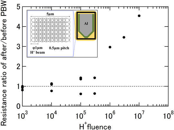
Another factor is a variation in the amount of current injected into the VSi. To verify this, we checked for an effect of PBW on sample resistance. A framed rectangle with thick line (5 μm in width) surrounding over the electrode for n+-type layer, as shown in the inset of Fig. 6, was drawn on the p-type layer by PBW with H+ fluence ranging from 3 × 10⁴ to 3 × 10⁷ H+/line, instead of a dot pattern. This line acts as a shield wall against current flow. Figure 6 shows the ratio of resistance after PBW with respect to that before PBW as a function of H+ fluence. The ratio is almost one up to a fluence of 3 × 10⁵ H+, indicating no change of resistance. Then, it increased with increasing H+ fluence. These results are in good accordance with the change of EL intensity including saturation behavior. However, this change was small compared with the degradation of emission efficiency. The shield wall was located at 4 μm below the sample surface (comparable to the VSi depth), which means that current flowing near the surface is not hindered. In addition, with increasing H+ fluence, the current tends to flow more preferentially in unirradiated areas with lower resistance. In this case, a large amount of current flows in the unirradiated area because the ratio in width of the unirradiated and the irradiated areas is 9. It is notable that measurements were conducted under constant current conditions. Considering these geometric aspects, the resistance of p-layer around VSi was estimated to be quite large after PBW. Therefore, we conclude that the decrease of emission efficiency was mainly caused by a decrease in the amount of injected current into VSi due to defects acting as majority carrier removal centers (highly resistive region) introduced by PBW.
The ratio of resistance after PBW with respect to that before PBW at a forward bias of 7 V as a function of H+ fluence. The trend of resistance change is in good accordance with the EL result [Fig. 5(a)] including saturation behavior. The inset shows that a framed rectangle with a 5 μm width thick line used to verify an effect of PBW on resistance of the p-layer. A thick line consisted of 0.5 μm pitch dot pattern designed to irradiate a whole line area by H+ beam with 1 μm diameter, which surrounded over the electrode for the n+-type layer to act as shielding current flow between electrodes.

By contrast, for PL as shown in Fig. 5(b), the intensity linearly increased up to 1 × 10⁶ H+/dot for all tested laser powers (0.1, 0.6, and 2.0 mW). Deviation from linearity, shown as dashed lines was observed for only fluence above 3 × 10⁶ H+/dot. However, the deviation from a linear increase is smaller than that for EL. As discussed in the case of EL, the balance of A and B was not a main reason for the results. Since the irradiation region was directly excited by photons, the highly resistive region had little influence on emission efficiency in contrast to EL. In the heavy irradiation region (above 3 × 10⁶ H+/dot), residual defects which act as nonradiative centers introduced by PBW can potentially explain the behavior observed in the PL measurements. Such defects existing in close vicinity to VSi dissipate electrons excited by photons, instead of VSi, leading to less intensity of luminescence from the irradiated area. The amount of dissipation is expected to be proportional to the concentration of nonradiative centers. The shorter the distance between the nonradiative center and the VSi corresponds to a higher concentration of nonradiative centers leading to an increase of dissipation in nonradiative centers. This is likely the cause of the degradation in the emission efficiency.
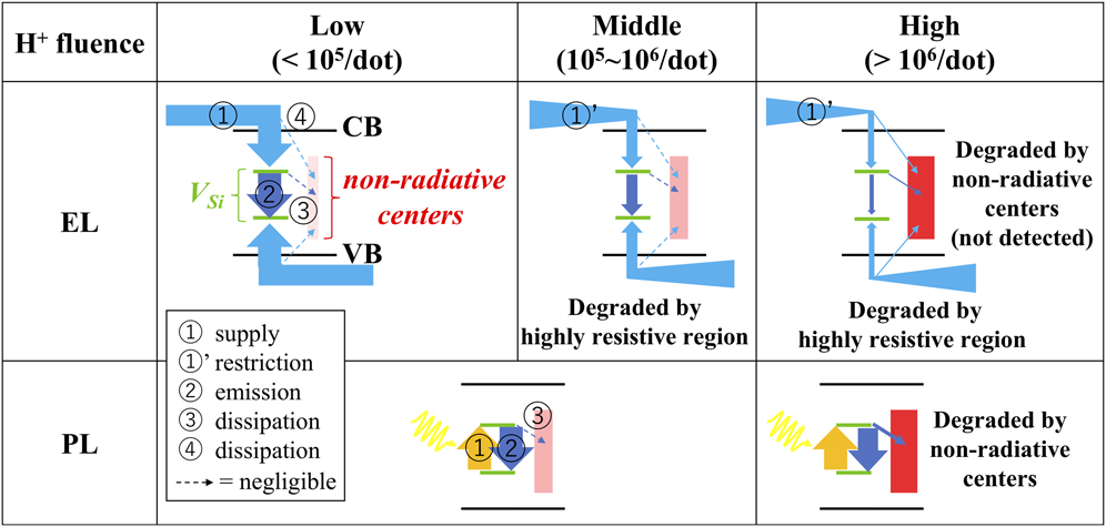
As discussed above, the emission efficiency of EL is much different from that of PL. This is attributed to a difference of the VSi excitation mechanism. Figure 7 summarizes the factors that degrade the emission efficiency of EL and PL with respect to H+ fluence. For low fluence (<105 H+/dot), no degradation by the highly resistive regions and nonradiative centers occurs in the case of either EL or PL. For EL, the degradation of emission efficiency can be observed at middle fluence (105–106) by the restriction of the amounts of electrons and/or holes to be supplied to VSi caused by the highly resistive region since the highly resistive regions have an influence on the entire current pathway [a narrowing width of arrows indicates the restriction (process 1′)]. By contrast, no degradation was observed for PL. For high fluence (>106 H+/dot), more degradation by the highly resistive region occurred for EL (process 1′). In addition, degradation by nonradiative centers emerges (process 3 and 4). At this fluence, the PL emission efficiency is degraded by nonradiative centers (process 3). This suggests that the current pathway should be taken care of, in addition to the creation of VSi. In this regard, PBW is a favorable method compared with conventional methods such as broad beam and whole area irradiation in which defects acting as majority carrier removal centers (highly resistive region) and nonradiative centers are created at undesired locations.
The factors that degrade the emission efficiency of EL and PL with respect to H+ fluence. Process 1: supply of carriers by current or photoexcitation. Process 1′: restriction of the amounts of electrons and/or holes to be supplied to VSi on the entire current pathway by the highly resistive region. Process 2: emission at VSi. Process 3: dissipation of carriers by nonradiative centers via the VSi state. Process 4: dissipation of carriers by direct transition to nonradiative centers. Dotted arrows indicate the negligible process. Influence of crystalline damage introduced by PBW emerges at more than 1 × 10⁵ H+/dot. The higher resistive region degrades EL emission efficiency at more than middle H+ fluence due to the restriction of the amounts of electrons and/or holes (Process 1′). Degradation of PL emission efficiency is led by nonradiative centers at high H+ fluence.

The findings obtained in this study are necessary fundamental information needed to realize quantum sensors using VSi. The highly resistive region is harmful for not only to the excitation of the VSi but also normally working devices. The former results in less sensitivity of sensors. The latter causes an inaccurate sensing even though a quantum sensor using VSi operates normally. Although the effect of nonradiative centers for EL is not detectable due to the highly resistive region in this study (process 4 for EL at higher fluence in Fig. 7), a decrease of nonradiative centers is also a problem, which needs to be solved if the introduction of the highly resistive region can be avoided. Therefore, further improvements of the process to introduce VSi without the highly resistive region and nonradiative centers is required.
IV. CONCLUSIONS
We investigated the optical properties of electrically excited VSi fabricated in the SiC pn junction diode by PBW. Characterizations suggest that PBW successfully introduced electrically controllable VSi into the device with no significant degradation of diode performance. The dependence of the EL and PL intensities from VSi on H+ fluence revealed that the emission efficiency of EL is less than that of PL. Saturation of emission intensity for EL was observed above 1 × 10⁵ H+/dot, but was not observed for PL. This is caused by a difference of VSi excitation mechanism because supply of carriers (electrons and/or holes) was restricted for EL due to the highly resistive region introduced around VSi by PBW. By contrast, electrons are directly excited by photons, leading to higher efficient emission for PL compared with EL. These results suggest that further improvements of the process to introduce VSi without the highly resistive region and nonradiative centers by optimization of PBW conditions are key points to realize highly sensitive quantum sensors using VSi.
ACKNOWLEDGMENTS
This study was partially supported by JSPS KAKENHI Grant No. 17H01056. Part of this study was carried out under the framework of IAEA CRP F11020. This study was partially supported by KIST Open Research Program (2E27231). We would like to appreciate Dr. Wataru Kada of Gunma University for the support on PBW experiments.