I. INTRODUCTION
Point defects often act as color centers in semiconductors where we use the phrase “semiconductor” in a broader context. For instance, it includes germanium crystal with small gap of ≈0.7 eV and diamond with large gap of ≈5.5 eV. Electrically active point defects introduce defect levels in the fundamental gap of semiconductors. An incident photon may excite an electron from the valence band (VB) into the defect level or from the occupied defect level to the conduction band (CB). This is the band-to-defect level or defect level-to-band excitation. When two defect levels occur in the gap then defect level-to-defect level excitation may also take place, which can be more effective than transitions between defect levels and bands. In all these processes, the light absorbed is at lower energies (i.e., at larger wave lengths) than that in pristine semiconductors, so point defects can change the “color” of the host semiconductors, nevertheless, not necessarily in the visible range of the spectrum. Spectroscopy tools involve the use of very sensitive methods [such as absorption or photoluminescence (PL)] that can show the fingerprints of these color centers in the corresponding spectra even if the concentration of the point defects responsible for the signal is relatively low. Color centers are usually effective electron or hole traps that can seriously deteriorate the operation of semiconductor devices, thus the identification of these color centers is of high importance. Besides the traditional application in electronic devices, there is a fast emerging field of quantum optics where paramagnetic isolated color centers or other point defects in semiconductors may play a crucial role: accomplishing the solid state quantum bit or qubit. The detailed knowledge about the ground and excited states of color centers is crucial for this special application. Accurate ab initio calculations may contribute to identification and characterization of color centers where the nature of their excitation can be understood. Recent advances in methodologies and algorithms have made possible to address this challenging issue.
Due to the size limitation of this paper, we do not provide comprehensive or detailed description about the ab initio methods in the following section, but we summarize briefly the investigations and recent results on point defects in semiconductors that have been obtained by the author. We defer the readers to the literature for detailed description of the methods but we rather focus on the application of methods. Nevertheless, we show some equations in our paper where we use atomic units.
II. METHODOLOGY
Density functional theory (DFT) has been proven to be an extremely powerful method to study defects in solids. Nowadays, application of DFT is a standard tool to investigate the concentration of defects in solids in thermal equilibrium, their interaction with each other, their vibration modes, or their hyperfine tensors.Reference de Walle and Neugebauer1–Reference Umeda, Son, Isoya, Janzén, Ohshima, Morishita, Itoh, Gali and Bockstedte5 All these properties are associated with the ground state of the defect. The success of the DFT calculations are based on the well-developed approximate (semi) local functionalsReference Ceperley and Alder6–Reference Perdew, Burke and Ernzerhof9 that made it possible to study relatively large systems at moderate computational cost with surprisingly good accuracy.
The success of the commonly used (semi) local functionals might be unexpected as they suffer from self-interaction errorReference Perdew and Zunger7 resulting in underestimation of the band gap of semiconductors. We call this for brevity as “band gap error.” In pathological cases, (semi) local DFT functionals predict no gap for pristine semiconductors. A typical example is germanium crystal. This ab ovo stems to study point defects in infinite Ge crystal that can be modeled by supercell method in which the defect is embedded into a cluster with periodic boundary conditions,Reference Deák10 thus point defects in Ge crystal could only be modeled in Ge nanocrystals (also called molecular cluster models, see again Ref. Reference Deák10) where the gap is opened due to quantum confinement. The self-interaction error of DFT functionals should be a priori healed even for the ground state calculations in pathological cases. For many semiconductors, the “band gap error” is not so severe and (semi) local DFT supercell calculations could predict qualitatively well even the adiabatic (thermal) ionization energies of defects.Reference de Walle and Neugebauer1 Nevertheless, we have to note that quantitatively good accuracy is needed in the calculation of defect levels in the fundamental gap to determine their excitation energies.
A. “Band gap error” and hybrid density functionals
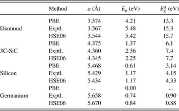
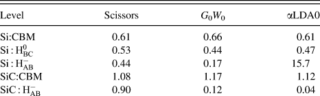
The “band gap error” is particularly problematic in wide-band-gap semiconductors when quantitative analysis is needed. For instance, this error is ≈1 eV for 3C-SiC while it is only ≈0.5 eV for Si crystal (see Table I). If the defect states are well localized then the absolute error in the position of the defect levels in the fundamental gap with respect to valence band maximum (VBM) could be much smaller in Si than in 3C-SiC. This ultimately calls for such methods that can rectify the “band gap error” in wide-band-gap semiconductors such as SiC or diamond.
As a first attempt, we began by applying an empirical “scissors correction” to eliminate the “band gap error.” The idea is to take the VBM as reference, open up the gap to its experimental value, and apply a “scissors operator,” introduced by Baraff and SchlüterReference Baraff and Schlüter11 for the case of vacancy defects. Since the wave function of the defect can be expanded on the basis of the perfect crystalline states, they assumed that the amount of shifting that is necessary for a given defect level can be determined by the weight of the CB states in the expansion. Therefore, the shift necessary for the conduction band maximum (CBM) to reproduce the experimental gap is to be scaled by the sum of overlaps between the defect wave function and all CB states of the perfect crystal. We first applied this procedure for vacancy- and hydrogen defects in SiC.Reference Aradi, Gali, Deák, Lowther, Son, Janzén and Choyke12 In our experience, the scissors operator has worked reasonably well for substitutional defects and split-interstitials or bond center sites but for interstitial defects in the low electron density region of the crystal (such as antibonding sites) the results seemed to be problematic. We checked the validity of “scissors operator” by a semi empirical quasiparticle correction (see next paragraph and Table II). The variable success of “scissors correction” can be explained by the fact that the VB states of the perfect crystal do not provide an adequate basis for expanding a strongly localized defect state in a low electron density region of the host crystal.Reference Deák, Frauenheim and Gali13
A more accurate correction of the Kohn-Sham defect levels in the gap would come from the many-body perturbation theory (MBPT). A common procedure to apply the GW approximation of MBPTReference Hedin and Lundqvist14 where i GW would give the quasiparticle correction energy to the DFT exchange-correlation energy, where G and W stand for the Green-function and the many-body screened Coulomb-interaction between electrons, respectively. In practice, GW approximation is applied as a single shot, G 0W 0, so G and W are not calculated self-consistently. Even G 0W 0 calculation is very cumbersome for supercells consisting of more than few tens of atoms. From 2004, we applied G 0W 0 quasiparticle correction to various point- and extended defects in SiC with using a so-called plasmon-pole approximation and a model dielectric functionReference Furthmüller, Cappellini, Weissker and Bechstedt15 where we could apply this method for supercells consisting of 64–128 atoms. By that way, we could check the validity of “scissors operator” for vacancy and interstitial defects (see Table II). The increasing computational power and efficient algorithms have recently allowed us to apply parameter-free ab initio G 0W 0 quasiparticle corrections for the negatively charged nitrogen-vacancy (NV) defect in diamond in a 256-atom supercell.Reference Ma, Rohlfing and Gali16 We are also aware of a recent study on the excitation property of carbon vacancy in 4H-SiC in a 288-atom supercell.Reference Bockstedte, Marini, Pankratov and Rubio17 Nevertheless, such calculation is still at the limit of computational power and time, thus an alternative method is needed to carry out defect calculations in semiconductors to a large extent.
For this reason, we applied non local hybrid functionals to obtain defect levels in the gap free from the “band gap error” from 2002. The pioneer study of non local hybrid functionals on point defects in semiconductors was published in 2003Reference Gali, Deák, Ordejón, Son, Janzén and Choyke18, Reference Gali, Deák, Rauls, Son, Ivanov, Carlsson, Janzén and Choyke19 and forthcoming years.Reference Deák, Gali, Sólyom, Buruzs and Frauenheim20–Reference Rurali, Aradi, Frauenheim and Gali27 At that time, the option of hybrid functionals within periodic boundary conditions was available in crystal code.Reference Saunders, Dovesi, Roetti, Causá, Harrison, Orlando and Zicovich-Wilson28 That particular code was developed on a basis of Hartree-Fock (HF) method together with Gaussian type orbital basis set where DFT method was later incorporated. We applied a single parameter hybrid functional,

where α is the mixing parameter of the HF-exchange and DFA is the actual approximation of the exchange-correlation functional of DFT. We applied α = 0.20 with DFA = local density approximation (LDA) for calculating point defects in silicon carbide (SiC). This particular choice reproduced the band gap of Si and different polytypes of SiC.Reference Gali, Deák, Ordejón, Son, Janzén and Choyke18 Originally, Becke suggested this functional, and he found that the choice of 0.16 ≤ α ≤ 0.28 reproduce the ionization energies and other properties of molecules in G2 set.Reference Becke29 Perdew et al. later found that α = 0.25 should be an optimal choice derived from the perturbation theory of coupling constant integration, and DFA = PBE will provide superior results for the molecules in G2 set over the other hybrid functionals containing three or more parameters.Reference Ernzerhof and Scuseria30 This functional is often called PBE0 functional. If α ≠ 0.25 and is optimized for reproducing the band gap of a given semiconductor then it may be labeled as αPBE0.
The HF-exchange is essentially Coulomb-interaction (1/r), which may decay and converge very slowly in solids. It was proposed that a screened Coulomb integral could solve this problem.Reference Heyd, Scuseria and Ernzerhof31, Reference Heyd and Scuseria32 By introducing the inverse of screening length (ω), the Coulomb-interaction can be decomposed in to short-range [S ω(r)] and long-range [L ω(r)] terms,

where r = |r - r′|, erfc (r) and erf(r) are the complementary and plain error functions, respectively. 2/ω corresponds to the characteristic length where S ω(r) decays to zero. Then, PBE0 functional was modified to

where (sr) and (lr) labels the short-range and long-range functionals, respectively. This is called HSE functional. According to the most recent analysis, ω = 0.11 bohr−1 ≈ 0.2 Å−1 provides the best results for selected molecules, which is called HSE06 functional. This functional has been implemented in the plane wave supercell codes vaspReference Kresse and Hafner33, Reference Kresse and Furthmüller34 and pwscfReference Giannozzi, Baroni, Bonini, Calandra, Car, Cavazzoni, Ceresoli, Chiarotti, Cococcioni, Dabo, Dal Corso, de Gironcoli, Fabris, Fratesi, Gebauer, Gerstmann, Gougoussis, Kokalj, Lazzeri, Martin-Samos, Marzari, Mauri, Mazzarello, Paolini, Pasquarello, Paulatto, Sbraccia, Scandolo, Sclauzero, Seitsonen, Smogunov, Umari and Wentzcovitch35 making the high quality hybrid density functional supercell calculations possible. According to recent calculations, HSE06 functional could very well reproduce the experimental band gap of small- and medium-gap semiconductorsReference Marsman, Paier, Stroppa and Kresse36 (see also Table I) and band alignmentsReference Wadehra, Nicklas and Wilkins37 without tuning either the mixing or the screening parameters. In addition, our study on selected point defects in Group-IV semiconductors showed that their thermal ionization energies could be well reproduced with HSE06 functional across the materials with small gap (Ge) and large gap (diamond).Reference Deák, Aradi, Frauenheim, Janzén and Gali38 We note that optimized αPBE0 and HSE06 functionals provide very similar results on defect levels in the gap of a given semiconductor according to a recent study.Reference Komsa, Broqvist and Pasquarello39 This makes the hybrid functionals promising methods for mimicking a self-consistent quasiparticle correction (see also Table II) and to use them as starting point for excitation calculations. The HF-exchange is a non local functional consisting of four-center integral of Kohn-Sham states. Thus, the computational need is about an order of magnitude larger than that by traditional (semi) local functionals but it is still a faster method than GW-method. An additional advantage of hybrid functional over GW-method is that the forces can be calculated in a straightforward manner. Thus, hybrid density functional calculations are good compromise to obtain relatively accurate quasiparticle energies and states until we reach the computational power and capacity to apply parameter-free MBPT methods in production.
B. Beyond the mean-field approximation: time-dependent DFT
The quasiparticle energies and states are still within the mean field approximation. To calculate the excitation spectrum properly, one must go beyond the mean field approximation. Time-dependent DFT (TD-DFT) goes beyond this approximation.Reference Casida and Chong40 The kernel of TD-DFT may be given within linear response theory as
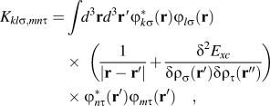
where φ are Kohn-Sham orbitals with particle indices of k, l, m, n and spin indices of σ, τ. It is important to notice the many-body nature of the TD-DFT kernel where two particle indices (k, l) are associated with occupied Kohn-Sham states while the other two particle indices (n, m) refer to unoccupied Kohn-Sham states. The kernel consists of two parts in the parentheses: the Hartree part is local in time (it causes the so-called local field effects) and provides the spectrum within random phase approximation (RPA). The second part of the kernel is generally non local both in space and in time. In the adiabatic approximation (which is always used in practice), it is time-independent but still space-dependent as apparent from Eq. (4). By setting up the corresponding Casida’s equations with the help of this kernel one can take into account the antiresonance between the occupied and unoccupied orbitals. The neglect of antiresonance is called Tamm-Dancoff approximation.Reference Casida and Chong40 We note that electron-hole interaction beyond RPA is often labeled as 
Bethe-Salpeter equation (BSE) is an alternative method to calculate the excitation spectra that relies on many-body perturbation method in the framework of GW-formalism. We present GW + BSE results on NV center in a supercell model, thus we briefly describe this formalism in conjunction with TD-DFT method. Formally, BSE kernel is very similar to TD-DFT kernel in Eq. 4, but the screened Coulomb interaction, W(r, r′), must be subtracted instead of adding f xc(r, r′) in the second part of the kernel and the wave function indices are kn; lm instead of kl; nm because two-particle exciton wave functions, which comprised both occupied and unoccupied wave functions, are used in BSE formalism. Another important issue is that the quasiparticle energies appear in the GW + BSE formula while DFT energies are present in the TD-DFT formula. We apply hybrid density functionals in the TD-DFT kernel, which may be viewed as a “crude” way of quasiparticle correction to (semi) local DFT. In this sense, the basic difference between the two methods is the treatment of the electron-hole interaction in the kernel, i.e., f xc(r, r′) versus –W(r, r′). A detailed study on comparison of BSE and TD-DFT method can be found in Ref. Reference Reining, Olevano, Rubio and Onida41. We will focus on the application of TD-DFT method on defects in semiconductors in this paper.
TD-DFT method has been successfully applied recently to calculate the excitation spectrum of molecules and semiconductor nanocrystals.Reference Onida, Reining and Rubio42 In some earlier studies, efforts have been made to address the excitation of defect states in solids by TD-DFT method where “solids” were modeled by extremely small finite clusters including 5–50 host atoms.Reference Uchino, Takahashi and Yoko43–Reference Zyubin, Mebel, Hayashi, Chang and Lin47 However, it is very questionable whether the electron states associated with the defect in a solid are properly described in such small clusters, and no thorough study has been carried out so far even for a single defect to address this very important issue. We note that TD-DFT excitation spectrum obtained by (semi) local functionals is reliable only for finite structures.Reference Onida, Reining and Rubio42 In a very recent study, it has been shown that hybrid density functional in the TD-DFT kernel provides appropriate excitation spectrum for infinite semiconductors.Reference Paier, Marsman and Kresse48 Here, we restrict ourselves to finite structures where both the local and the non local functionals can be consistently applied and validate the results for bulk systems. We study three representative defects in wide gap semiconductors: NV center in diamond, Si-vacancy, and divacancy in SiC. A common behavior of these defects is that they produce characteristic transition in the PL spectrum.
C. Applied models and methodology on selected point defects
In bulk system, the calculations were carried out in large 512-atom supercells using either LDA,Reference Ceperley and Alder6 PBE,Reference Perdew, Burke and Ernzerhof9 or HSE06Reference Heyd and Scuseria32 functionals with Γ-point sampling of the Brillouin zone. This ensures the convergence of charge density and enables monitoring of the degeneracy of defect levels. We used the computationally expensive VASP code with plane wave basis set with a plane wave cut-off of 420 eV (≈30 Ry) which is highly convergent with the applied projected augmentation wave projectors for carbon, nitrogen, hydrogen and silicon atoms.Reference Blöchl49, Reference Kresse and Joubert50
In nanocrystal studies, we embed the defects into a nanocrystal that contains 147 host crystal atoms and 100 hydrogen atoms for termination. We applied PBEReference Perdew, Burke and Ernzerhof9 functional to optimize the geometry while the excitation spectrum is calculated both by the semi local PBE and by the non local hybrid PBE0 functionals. The optimization of the geometry has been done with numerical atomic basis set for diamond nanocrystal at double ζ polarized (DZP) level which provided good results in supercells as compared with plane wave calculations.Reference Gali, Fyta and Kaxiras51 We used the SIESTA code for this purpose in diamond studies.Reference Sanchéz-Portal, Ordejón, Artacho and Soler52 Troullier-Martins pseudopotentials have been applied to model the effect of nuclei together with the core electrons in SIESTA calculations.Reference Troullier and Martins53 We used the VASP code to study the divacancy in SiC. In the VASP calculations, we applied the appropriate symmetry, and the energy of the ground state and the excited states are calculated by setting the appropriate occupation of the defect states in the gap as explained below. In the geometry optimization calculations, all the atoms were allowed to relax until the forces were below 0.01 eV/Å.
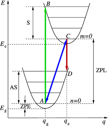
In VASP code, it is possible to set the occupation number of single particle states. This may be used to study the geometry change upon electronic excitation.Reference Gali, Fyta and Kaxiras51, Reference Gali, Janzén, Deák, Kresse and Kaxiras54 In this scheme, the excited state is described by promoting an electron from an occupied Kohn-Sham defect level to an unoccupied Kohn-Sham defect level of the ground state with allowing the nuclei to relax to find the optimum geometry with the charge density obtained from this fixed occupation of orbitals. This method is called constrained DFT briefly. The constrained DFT method is a computationally less expensive method to find the zero phonon line (ZPL) transition energy within the Franck-Condon approximation as shown in Fig. 1. In our experience, this methodology under special circumstances provides reliable results regarding the relaxation energy due to electronic excitationReference Gali, Janzén, Deák, Kresse and Kaxiras54 which is the Stokes shift shown in Fig. 1. The constrained DFT method may provide reliable results for the Stokes shift upon the following conditions:
(1) The excited state can well be described by a single Slater determinant and the symmetry of the ground and excited states are different thus avoiding possible hybridization of states.
FIG. 1.The energy (E) versus configuration coordinate (q) diagram for the excitation process of a defect in the Franck-Condon approximation: Eg, Ee are the minima in the quasi-parabolic potential energy surfaces of the defect in the ground and excited states, respectively and qg, qe the corresponding coordinates. ZPE is the zero point energy (indicated only for the ground state). The energy ladders show the phonon energies with the phonon ground states at n = 0 (ground state of the defect) and m = 0 (excited state). At elevated temperatures, the high-energy phonon states can be occupied by inducing transition A → B (vertical absorption, green arrow), and C → D (vertical emission, red arrow). Transition A ↔ C corresponds to the ZPL (blue double arrow) both in absorption and emission. The energy of the Stokes shift is the energy difference between vertical absorption and emission which is equal to the sum of the energies represented by S and AS that are the relaxation energies of nuclei upon photon absorption and emission, respectively.

(2) The nature of the excited and ground states is similar; for instance, they are originated from similar well-localized defect states.

Comparison of PBE and HSE06 resultsReference Deák, Aradi, Frauenheim, Janzén and Gali38 for the lattice constant a, fundamental (indirect) gap (Eg), first allowed direct transition at the Brillouin-zone center ( ) with experimental dataReference Madelung90, Reference Levinshtein, Rumyantsev and Shur91 in case of the Group-IV semiconductors

As we show below, we considered such defects here that can fulfill these criteria. Nevertheless, this statement cannot be proven by DFT-based methods alone. We studied the nature of excitation by TD-DFT method that is capable of studying the above-mentioned criteria. We applied the Turbomole package to carry out the TD-DFT calculations.Reference Ahlrichs, Bär, Häser, Horn and Kölmel55 This is a cluster code with localized Gaussian basis sets that can utilize hybrid functional in the TD-DFT kernel. We applied an all-electron Gaussian DZP basis set for all the atoms in the systemReference Schuchardt, Didier, Elsethagen, Sun, Gurumoorthi, Chase, Li and Windus56 at fixed coordinates supplied by Siesta or VASP DFT calculations. We calculated the adiabatic TD-DFT spectrum both with spin-polarized semi local DFT-PBE and with non local PBE0 functionals within the linear response theory and beyond the Tamm-Dancoff approximation. We particularly focused on the lowest excitation energies that may be manifested in the low temperature absorption and PL spectra.
III. RESULTS AND DISCUSSION
A. NV center in diamond
NV center in diamond has attracted a lot of attention in recent years, since it has been detected at a single defect levelReference Gruber, Drabenstedt, Tietz, Fleury, Wrachtrup and Borczyskowski57, Reference Drabenstedt, Fleury, Tietz, Jelezko, Kilin, Nizovtzev and Wrachtrup58 and provides a quantum bit for quantum computing applications.Reference Jelezko, Popa, Gruber, Tietz, Wrachtrup, Nizovtsev and Kilin59–Reference Hanson, Mendosa, Epstein and Awschalom63 Besides providing a single photon source for quantum cryptography,Reference Brouri, Beveratos, Poizat and Gragier64, Reference Beveratos, Brouri, Gacoin, Poizat and Grangier65 the NV center is also a promising candidate as an optically coupled quantum register for scalable quantum information processing, such as quantum communicationReference Childress, Taylor, Sørensen and Lukin66 and distributed quantum computation.Reference Jiang, Hodges, Maze, Maurer, Taylor, Cory, Hemmer, Walsworth, Yacoby, Zibrov and Lukin67 In addition, it has been recently demonstrated that proximal nuclear spins can be coherently controlled via hyperfine interactionReference Childress, Gurudev Dutt, Taylor, Zibrov, Jelezko, Wrachtrup, Hemmer and Lukin68 and used as quantum memory with an extremely long coherence time.Reference Gurudev Dutt, Childress, Jiang, Togan, Maze, Jelezko, Zibrov, Hemmer and Lukin69
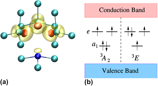
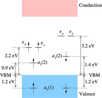
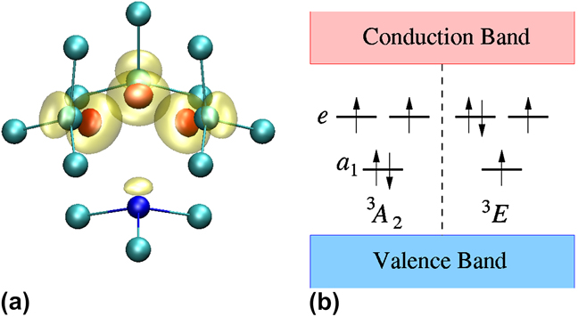
NV center consists of a substitutional nitrogen atom near a vacancy in diamondReference du Preez70–Reference Collins74 as Fig. 2(a) shows. The NV center has a strong optical transition with ZPL at 1.945 eV (637 nm) accompanied by a vibronic band at higher energy in absorption with the largest intensity at about 2.20 eV and lower energy in emission (Fig. 1). Detailed analysis of the ZPL revealed that the center has trigonal, C3ν symmetry.Reference Davies and Hamer71 Previous ab initio calculation clearly supported the negatively charged NV defect for 1.945 eV ZPL centerReference Gali, Fyta and Kaxiras51, Reference Goss, Jones, Breuer, Briddon and Öberg75, Reference Larsson and Delaney76 as was originally proposed by Loubser and van Wyk.Reference Loubser and van Wyk72 In the NV defect, three carbon atoms have sp 3 dangling bonds near the vacancy (with three back bonds in the lattice) and nitrogen atom has also three back bonds with one dangling bond pointing to the vacant site. Since nitrogen has five valence electrons, the negatively charged NV defect has altogether six electrons around the vacancy. One can use the defect-molecule pictureReference Watts77 together with group theory to find the canonical orbitals of this system. According to this analysis, there are two fully symmetric one-electron states (a 1) and one doubly degenerate e state, which should be occupied by 6 electrons.Reference Gali, Fyta and Kaxiras51 It was found that the two a 1 states are deeper in energy than the e state. As a consequence, four electrons occupy the a 1 states and two electrons remain for the e state. Our calculated Kohn-Sham levels obtained by ab initio supercell calculations are shown in Fig. 3. As can be seen in Fig. 3, the natural choice is to put the two remaining electrons parallel to the e level forming an S = 1 state (in analog to satisfy the Hund rule for the p -orbitals of the isolated Group-IV elements in the periodic table). In the C3ν point group this total wave function has 3A 2 symmetry, where 3 = 2S + 1 with S = 1. In our special case, we chose the M S = 1, so both electrons are spin-up electrons on the e level. As can be seen, again in Fig. 3, the lowest a 1 level is relatively deep in the VB, so it seems to be a good approximation to assume that it does not contribute to the excitation process, and we do not consider it further. However, the next a 1 level in the gap is not very far from the e level. If one electron is excited from the this a 1 level into the e level then one will arrive at 3E state [Fig. 2(b)]. The 3E is a doubly degenerate many-electron state, so it comprises two orthogonal many-electron states with the same eigenenergy. Both of them can be described by a single Slater determinant: if the electron from a 1 level is promoted to ex then the symmetry of the resulted many-electron state will be Ex , if it is promoted to ey then the resulted many-electron state will be Ey . Thus, Fig. 2(b) shows one of the true M S = 1 eigenstates of the excited state under C 3ν symmetry (see Ref. Reference Gali, Fyta and Kaxiras51 and references therein).
(a) The structure of N − V − center in diamond; only first- and second-neighbor C (cyan spheres) and N (blue sphere) atoms to the vacant site are shown. The yellow and red lobes are contours of the calculated spin density. (b) Schematic diagram of the defect states in the gap and their occupation in the 3A 2 (ground) and 3E (excited) states.
The calculated Kohn-Sham levels with respect to the VBM in the ground state of the NV defect. The results obtained in a 512-atom supercell by LDA functional in Ref. Reference Troullier and Martins53.

Comparison of the scissors- and the G 0W 0 quasiparticle corrections to the Kohn-Sham levels obtained by LDA functional for interstitial H in Si and 3C-SiC
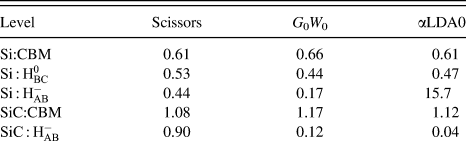
Also, corrections predicted by a one-parameter hybrid functional αLDA0 with α = 0.20 are given where α is the fraction of Fock-exchange in the LDA exchange-correlation functional (see text for more details) which reproduce the band gaps of 3C and 4H-SiC as well as of Si. All units are in eV. Carbon vacancy was calculated in 4H-SiC at cubic site. We give the correction of the occupied defect level of carbon vacancy published first here. The other data were already published in Ref. Reference Ma, Rohlfing and Gali16.
The only allowed transition is 3A 2 → 3E in the first order. Thus, the excitation of this system may be explained by promoting an electron from the a 1 single particle state to the e state resulting in the 3E excited state. In this picture one may apply the constrained DFT calculation with ΔSCF procedure to obtain the excitation energy. The calculated value may be directly compared with the experimental data if the corresponding defect levels are at quasiparticle levels free from the “band gap error” of (semi) local functionals. We utilized first the screened hybrid HSE06 functional for pristine and defective diamond supercell. Our calculations reproduced the experimental vertical energy of absorption (2.20 eV) as well as the ZPL energy (1.94 eV) very accurately. Similar results have been later obtained by Weber et al.Reference Weber, Koehl, Varley, Janotti, Buckley, de Walle and Awschalom78 in a smaller supercell for NV-center and they applied this method to study some defects in hexagonal SiC.
Despite the success of this method, the aforementioned picture of excitation is certainly oversimplified since the excited electron senses the presence of the hole left behind as a result of the Coulomb interaction between them, so they cannot be treated separately. Correspondingly, the wave function in the excited state, which should describe the motion of the correlated electron-hole pair, is principally not given by a simple product of electron and hole wave functions but requires a more general representation to account for energetic and spatial correlation between the two particles. Thus, we examine the excitation of NV center by TD-DFT theory, which is able to address this complex phenomenon. As explained above we apply TD-DFT in finite systems, which is the nanodiamond in this case.
An effective quantum confinement may be expected in nanodiamonds; however, the gap opens up only slightly by about 0.1 eV even in our relatively small nanodiamond with a diameter of about 1 nm as compared with that of bulk diamond. Recently, we have foundReference Vörös and Gali79 that nanodiamond exhibits low-lying Rydberg states, which results in only a small variation between the highest occupied molecular orbital (HOMO) – lowest unoccupied molecular orbital (LUMO) gap of nanodiamonds on the one hand and the band gap of bulk diamond on the other. This will have a serious consequence on the TD-DFT spectrum of NV-center as we will show below.
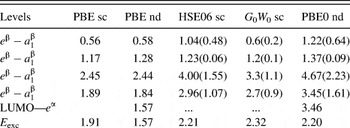
We started with the geometry optimization of the negatively charged NV center by SIESTA DFT-PBE calculations using spin-polarization and without symmetry restriction. The defect automatically arrived at the S = 1 state and retained the C3ν symmetry. It may be worthwhile to compare the relative positions of the defect states obtained in nanodiamond (labeled as “nd”) and supercell (labeled as “sc”) DFT-PBE calculations. Two defect levels appear in the HOMO–LUMO gap: the a 1 and e levels like in the supercell calculations. By comparing the PBE single particle Kohn-Sham levels obtained in the supercell and nanodiamond (columns 2 and 3 in Table III) we observe that the relative positions of the defect levels are very similar including the spin-polarization between  and
 states or the energy difference between a 1 and e states within the same spin channel. This implies that the defect levels are “fixed” relative to each other and do not change significantly by confining the crystalline states. In our supercell calculations we foundReference Gali, Fyta and Kaxiras51 that these defect states are strongly localized around the core of the defect, in other words, they “split” from the extended crystalline states that are not affected heavily due to quantum confinement. The results obtained in the nanodiamond model may be relevant for crystalline environment as the excitation may occur among the localized defect states.
Next, we may check the quasiparticle shift due to non local functionals or by G 0W 0 correction.Reference Hedin and Lundqvist14, Reference Ma, Rohlfing and Gali16 In the case of nanodiamond we used unscreened hybrid PBE0, which gave us very accurate absorption spectra for tiny nanodiamonds.Reference Vörös and Gali79 We believe that the unscreened hybrid functionals are more realistic for relatively small nanoclusters and molecules where the electron system cannot effectively screen the Coulomb potential like in an infinite crystal. By comparing the “HSE06 sc” and “PBE0 nd” columns we found that the quasiparticle shifts between occupied levels are very similar being only a bit (≈0.16 eV) larger for “PBE0 nd.” However, there is a larger difference between the relative positions of the unoccupied e β and the occupied states with the two methods. The quasiparticle shift for the unoccupied state is larger with the unscreened PBE0 functional, which may be a natural consequence of the larger HF-exchange term in the Hamiltonian. The G 0W 0 supercell calculations have been carried out at the Γ-point in 256-atom supercellReference Ma, Rohlfing and Gali16 which may not be fully convergent for the single particle states but still it is worthwhile to compare the G 0W 0 quasiparticle levels with those obtained by hybrid functionals. The spin polarization of a 1 state (≈ 0.2 eV) is not enhanced to such a large extent as compared with the same computed using hybrid functionals (0.5–0.6 eV) after the quasiparticle correction. Interestingly, the quasiparticle shift difference relative to  is also larger for HSE06 sc than for G 0W 0 sc, thus the quasiparticle shift difference for (
 ) will be similar.
Now, we turn to the investigation of the excitation energies. In the case of the TD-DFT calculation with PBE kernel we arrived at a very low value of 1.57 eV. According to our analysis the e α → LUMO transition is responsible for this absorption peak. As can be inferred in Table III, the energy of LUMO is indeed close to the energy of the highest occupied spin-up defect level e α. Apparently, this transition cannot occur in crystalline environment. The next lowest transition energy is about 1.88 eV, which is close to the lowest excitation energy calculated in the supercell by ΔSCF method (PBE sc column in Table III). However, this excitation peak arises in only 39% from  transition but 57% from e α → LUMO + 1 transition. This indicates that the TD-DFT spectrum at PBE level cannot describe the nature of transition occurring in bulk diamond due to the low-lying empty Rydberg state of nanodiamond. We note that the calculated “exciton-binding energy” of the lowest excitation is practically zero, which is typical for TD-DFT spectrum with (semi) local functionals in the kernel. The situation for the TD-DFT calculation with PBE0 in the kernel is different. In PBE0, the LUMO level is about the same energy distance from the e α state as the energy difference between
 and e β levels. The lowest excitation energy is 2.20 eV, which is dominated by
 transition to the extent of as much as 92%. While the energy difference between these single particle states was large (3.45 eV) due to the large quasiparticle shift between these states relative to their PBE values (1.61 eV), the large excitonic effect (1.25 eV) could compensate this effect by providing an excitation energy (2.20 eV), which is very close to the experimental value. This number is also close to the values derived from HSE06 sc and G0W0 + BSE sc calculations (Table III). We believe that it is not a fortuitous coincidence. HSE06 sc gave less quasiparticle shift than PBE0 nd and correspondingly the “exciton-binding energy” in HSE06 sc is smaller than for PBE0 nd. In G0W0 + BSE sc calculation, we found the smallest quasiparticle shift with again smaller “exciton-binding energy”. The unscreened PBE0 functional may overshoot the “quasiparticle shifts” relative to the PBE values, but the large excitonic effect compensated this resulting in reasonable values for the excitation energies. This implies that the calculated “exciton-binding energies” of defects in nanocrystals cannot reveal the “exciton-binding energies” of defects in the bulk counterpart, but the calculated excitation energies may be accurate when subjected to careful choice of the model and inspection of the nature of transition. From this investigation, we can also conclude for NV center in diamond that the lowest excitation is indeed described by promoting an electron from the
 level to the e β level that can support the constrained DFT method to calculate the Stokes shift for the PL process applied in Refs. Reference Ma, Rohlfing and Gali16, Reference Gali, Janzén, Deák, Kresse and Kaxiras54. We note here that this transition describes the absorption of the light with perpendicular polarization to the symmetry axis which transforms as E irreducible representation in C 3ν point group. The parallel-polarized light transforms as A 1 under C 3ν point group. According to the selection rules, E polarization will be allowed for 3A 2 → 3E transition in the first order while A 1 polarization is forbidden. Our finding is in line with this group theory analysis.
B. Negatively charged silicon vacancy in SiC
Silicon vacancy in SiC is a subject of great interest due to its peculiar properties: in the ground state, it exhibits high-spin electronic state and shows luminescence in the near-infrared range at around 1.4 eV.Reference Sörman, Son, Chen, Kordina, Hallin and Janzén80, Reference Baranov, Bundakova, Soltamova, Orlinskii, Borovykh, Zondervan, Verberk and Schmidt81 Photo-induced electron paramagnetic resonance (EPR) studies indicate that an effective electron spin polarization can occur for the silicon vacancy in SiCReference Mizuochi, Yamasaki, Takizawa, Morishita, Ohshima, Itoh and Isoya82, Reference Mizuochi, Yamasaki, Takizawa, Morishita, Ohshima, Itoh, Umeda and Isoya83 and its PL signal can be detected even at room temperature.Reference Isono, Tajima, Hoshino and Sugimoto84 Despite recent efforts of understanding the nature of the silicon vacancy centers,Reference Baranov, Bundakova, Soltamova, Orlinskii, Borovykh, Zondervan, Verberk and Schmidt81, Reference Janzén, Gali, Carlsson, Gällström, Magnusson and Son85 still there is a debate about the nature of the luminescence. The detailed understanding of the excitation of silicon vacancy is necessary toward its application in quantum optics and quantum information processes. According to our group theory analysis, the negatively charged Si-vacancy should be considered in understanding the PL signals of this defectReference Janzén, Gali, Carlsson, Gällström, Magnusson and Son85 that we investigate by TD-DFT calculations.
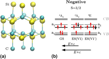
First, we studied the silicon vacancy in bulk 4H-SiC. We found that spin-polarized LDA of DFT (DFT-LDA) provided only a single a 1 and a single e level in the fundamental gap which are occupied by three electrons in negatively charged state with possessing high spin S = 3/2 state. These a 1 and e states are the split t 2 states of the vacancy in the low-symmetry crystal field of the hexagonal crystal. According to our previous group theory analysis,Reference Janzén, Gali, Carlsson, Gällström, Magnusson and Son85 another fully occupied a 1 level should exist in this defect that falls in the VB in DFT-LDA. In the negatively charged state of silicon vacancy, a generalized gradient approximation of DFT (DFT-PBE) showed the appearance of this low-lying a 1 state just above the VB in the minority spin channel (Fig. 4). HSE06 functional mimics the quasiparticle correction of DFT levels, which opens the gap by lowering the energy of the VB edge and increasing the energy of the CB edge. In HSE06 calculation, the appearance of the low-lying a 1 state in the gap in the minority spin channel (β electrons) is very clear and is even visible in the spin majority channel (α electrons) just above the VB edge. In addition, the order of the empty single particle levels is a 1 and e of the split t 2 level in the minority spin channel. The corresponding single particle energies at the cubic and hexagonal sites are equal within 0.05 eV, so the site dependence on the electronic structure of negatively charged Si-vacancy is not very significant, however, the different amount of splitting of the empty a 1 and e levels may cause different PL spectra at low and elevated temperatures.
(a) The optimized geometry of silicon vacancy in the ground state. Cyan and yellow balls represent C and Si atoms, respectively. (b) Schematic diagram about the defect states in bulk 4H-SiC in the 4A 2 ground and 4A 2, 4A excited states. VB and CB represent valence bands and conduction bands, respectively. The arrows show the luminescence processes with the corresponding polarization of the emitted light.

The relative positions of defect levels of NV center in the ground state in eV where α and β label the spin-up and spin-down channels, respectively.

The PBE and HSE06 supercell (sc) calculations have been carried out in 512-atom supercell yielding accurate excitation energies with HSE06 functional (Ref. Reference Gali, Janzén, Deák, Kresse and Kaxiras54) while G 0W 0 supercell calculations have been made in 256-atom supercell with about 0.15 eV larger excitation energies together with BSE than the experimental values (Ref. Reference Ma, Rohlfing and Gali16). “nd” labels the results obtained in our nanodiamond.  ,
 and e α states are occupied while e β is unoccupied in the ground state. LUMO is a Rydberg state in nanodiamond. The values in the parentheses are the relative quasiparticle corrections defined as the following: in column HSE06 sc this is the difference between column HSE06 sc and PBE sc carried out with the same size of supercell (but allowing relaxation with the two methods as explained in Ref. Reference Gali, Janzén, Deák, Kresse and Kaxiras54); in column G 0W 0 sc the reference PBE values are taken from the same geometry and supercell in Ref. Reference Hedin and Lundqvist14; in column PBE0 nd this is the energy difference between column PBE0 nd and PBE nd carried out in the same nanodiamond and with the same geometry. Lowest excitation energy (E exc) is calculated by ΔSCF method for PBE sc and HSE06 sc methods, while with G 0W 0 + BSE method for G 0W 0 sc and TD-DFT for PBE nd and PBE0 nd. Exciton-binding energy (E X) is defined as an energy difference between the calculated excitation energy and the quasiparticle energy difference between the corresponding states in TD-DFT methods while BSE provides this value on the top of G 0W 0 sc calculation.
In nano cubic 3C-SiC, the gap opens due to quantum confinement, therefore, the vacancy-related states are apparent even in DFT-PBE calculations. The order of single particle states closely follows that obtained in HSE06 calculations in bulk 4H-SiC. The PBE0 hybrid density functional also provided qualitatively the same single particle picture like DFT-PBE did. Next, we calculated the excitation energies by TD-DFT method based within PBE0 functional for the negatively charged silicon vacancy.
The excitation occurs in the spin minority channel between the occupied lower a 1 level and the empty upper a 1 and e levels (Fig. 4). The ground state is 4A 2 while the symmetry properties of the corresponding excited states are 4A 2 and 4E, respectively, with calculated excitation energies of 1.568 eV and 1.572 eV. In these processes, the selection rules may be applied and can be shown that the light would be only absorbed with polarization of parallel ( ) and perpendicular (
 ) to the symmetry axis, respectively. The calculated relaxation energy due to excitation is about 0.1 eV obtained by constrained DFT calculation, which puts the calculated zero-phonon line at about 1.47 eV.
In 4H-SiC V1, V1′ and V2 ZPL are associated with Si-vacancy where the corresponding optically detected magnetic resonance centers of Tv1a, etc. can also be detected. The transition energy of V1 and V1′ is at around 1.44 eV while it is at 1.35 eV for V2 where these ZPL signals may be associated with the inequivalent sites of Si-vacancy in 4H-SiC. According to detailed analysis, V1 (and V1′) may be associated with the cubic site.Reference Janzén, Gali, Henry, Ivanov, Magnusson, Son, Fleetwood, Pantelides and Schrimpf86 The emitted photons of V1 ZPL is polarized parallel to the symmetry axis while perpendicular to that in V1′ ZPL with about 4.5 meV of energy difference where V1 ZPL is lower in energy than that of V1′ ZPL.
The calculated properties of the negatively charged vacancy can all explain the experimental data, particularly, at k -site, which we model in nano 3C-SiC. The estimated ZPL is very close to the measured one, and the V1, V1′ ZPLs with the corresponding polarizations can be well explained by the selection rule of optical emission from the 4A 2 and 4E excited states, respectively (Fig. 4).
C. Divacancy in SiC
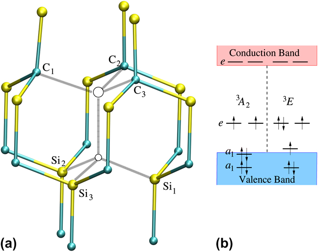
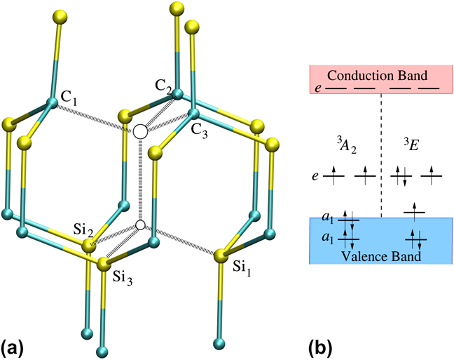
Divacancies are common defects in semiconductors with consisting of neighbor isolated vacancies. The divacancy has been recently identified in hexagonal SiC polytypes.Reference Son, Carlsson, ul Hassan, Janzén, Umeda, Isoya, Gali, Bockstedte, Morishita, Ohshima and Itoh4 The defect possesses C 3ν symmetry in cubic SiC and also at on-axis configurations in hexagonal polytypes. The silicon vacancy part of the defect (C1–3 atoms) introduces three carbon dangling bonds while the carbon vacancy part of the defect (Si1–3 atoms) contributes with three silicon dangling bonds (Fig. 5). Again, group theory analysis revealed usReference Janzén, Gali, Henry, Ivanov, Magnusson, Son, Fleetwood, Pantelides and Schrimpf86 that the six dangling bonds will build two a 1 and two e defect levels in C 3ν symmetry. Six electrons can occupy these states. According to our ab initio supercell calculations,Reference Janzén, Gali, Henry, Ivanov, Magnusson, Son, Fleetwood, Pantelides and Schrimpf86 the two a 1 levels are lowest in energy and then the doubly degenerate e levels follow them in the hierarchy. Four electrons will occupy the a 1 states and the two remaining electron will occupy the degenerate e level. Again, by following the Hund-rule the natural choice is to place the electrons with parallel spins. Indeed, the ground state of the neutral divacancy is a high spin S = 1 state.Reference Son, Carlsson, ul Hassan, Janzén, Umeda, Isoya, Gali, Bockstedte, Morishita, Ohshima and Itoh4, Reference Janzén, Gali, Henry, Ivanov, Magnusson, Son, Fleetwood, Pantelides and Schrimpf86 A PL spectrum of about 1.0 eV is associated with this defect, which can be also detected at low temperature infrared absorption in hexagonal SiC polytypes.Reference Magnusson and Janzén87 The nature of the excitation is not well understood.
(a) The optimized geometry of the divacancy in the ground state. Cyan and yellow balls represent C and Si atoms, respectively. The open circles depict the vacant sites. (b) Schematic diagram about the defect states in bulk 3C-SiC in the 3A 2 ground and 3E excited states. The upper e-level appears in the gap of bulk hexagonal SiC polytypes or nano 3C-SiC.
The position of the defect levels may reveal the possible excitation mechanism of the defect. We note here that CB edges of hexagonal polytypes of SiC lies about 1.0 eV higher than that of 3C-SiC polytype. In hexagonal polytypes, there are more than one configuration of divacancies. For the sake of simplicity, we discuss divacancy in 3C-SiC with a single configuration, which has C 3ν symmetry that may mimic the cubic environment in 4H-SiC.
In 3C-SiC, a double degenerate e defect level occurs in the fundamental band gap. The next localized and unoccupied e-level falls in the CB but appears in the gap of hexagonal polytypes. In the ground state, the lowest e level is occupied by parallel spin electrons. Two a 1 defect levels are in the VB where the highest a 1 state is resonant with the VB edge according to our ab initio supercell calculations in hexagonal polytypes.Reference Janzén, Gali, Henry, Ivanov, Magnusson, Son, Fleetwood, Pantelides and Schrimpf86 In 3C-SiC, spin-polarized PBE calculation shows an effective spin-polarization of the highest a 1 state that clearly appears in the gap in the spin minority (β) channel. The lowest e level also splits by about 0.5 eV while the empty e level does not split practically. One possible model to explain the excitation is to promote an electron from the resonant a 1 state to the lowest e level in the fundamental gapReference Janzén, Gali, Henry, Ivanov, Magnusson, Son, Fleetwood, Pantelides and Schrimpf86 [Fig. 5(b)]. This will result in 3A 2 → 3E excitation. The sharp excitation between a resonant state and a defect state in the fundamental gap is a well-known process in semiconductors, e.g., similar process takes place for the isolated vacancy in diamond.Reference Lowther88 Other excitations may also occur for divacancy in SiC, for instance, between the e defect levels in the gap of hexagonal SiC. We examine the lowest excitation energies of divacancy by TD-DFT calculations in nano 3C-SiC.
In the DFT-PBE cluster calculation, the “band gap” of nano 3C-SiC opens up with several eV as compared with their bulk counterpart.Reference Vörös, Deák, Frauenheim and Gali89 We note that we do not observe low-lying Rydberg states for SiC nanocluster like in diamond nanoclusters thus no such complications can occur in the analysis of the excitation spectrum of divacancy in SiC nanocrystals as for NV center in nanodiamond. Due to the increased gap of nano 3C-SiC, the excitation between e-levels can be studied in detail, which may occur in crystalline hexagonal polytypes. The quantum confinement of crystalline states makes the resonant a 1 state undoubtedly visible that is localized strongly on the carbon dangling bonds. Because this a 1 state does not mix with the crystalline states, therefore the spin-polarization of this a 1 state is significant (≈0.7 eV). The  state will push up the lowest empty e β state by about 0.5 eV, thus the energy difference between the lowest and highest e β states will be about 0.5 eV lower than in supercell calculation. It is important to notice that the relative position of the
 and e α states agree with those in supercell calculation within 0.1 eV. This may indicate that the localized resonant state also is in tune with the other localized defect states and splits from the crystalline environment. In the C 3ν symmetry, we determined the excitation energies with different light polarizations. As expected, the excitation with E polarization is lowest in energy which allows coupling of the 3A 2 ground state and the 3E excited state. Indeed, in this case the excitation between
 and lowest e β states is dominant, however, there is a non-negligible contribution (13%) from the lowest and highest e α states. The calculated absorption energy is 1.15 eV that is close to the measured ZPL transition of 1.0 eV. For the excitation with E polarization, we obtained 1.43 eV, which occurs between the lower and higher e α defect states. We note that the corresponding “exciton-binding energy” is zero as we found already for NV center in diamond.
Next, we studied this excitation by applying PBE0 hybrid functional in the TD-DFT kernel. The relative position between the occupied  and e α defect levels remains about the same (≈0.7–0.8 eV). However, the energy differences between the lower occupied and higher empty e α states and between the occupied
 and empty e β states are increased by about 1.7–1.8 eV. This quasiparticle shift is a natural consequence of the Fock operator in the hybrid functional which opens the gap between the occupied and unoccupied states. Again, we calculated the lowest excitation energies with A 1 and E polarizations. The excitation energy with E polarization is 1.18 eV, which almost coincides with the value obtained by the (semi) local PBE in the TD-DFT kernel. The basic difference between the two transitions that in TD-DFT with PBE0 in the kernel the transition is dominated (over 95%) by promoting the electron from the single particle
 defect level to the lowest e β level. The relative quasiparticle shift of about 1.8 eV was largely compensated by the excitonic effect of about 1.0 eV. Interestingly, the next excitation energy of 1.85 eV is due to the transition between the
 state and the higher e β state. The “exciton-binding energy” of this process is again ≈1.0 eV. The following excitation energy of ≈2.35 eV is caused by transitions of E, A1 polarizations between the lower occupied and higher empty e α defect states where the resulting “exciton-binding energy” is smaller (≈0.8 eV).
We calculated the Stokes shift due to electronic excitation by constrained DFT method. First, we studied the lowest excitation energy for which the transition between  and the lower e β states is the dominant process resulting in the 3E excited state as shown in Fig. 5(b). We set this occupation for the defect states and restricted the geometry optimization within C 3ν symmetry. The calculated Stokes shift is 0.075 eV. Because the e β state is half occupied, Jahn-Teller distortion may occur. By allowing C 1h geometry optimization, we obtained a slightly deeper energy than for C 3ν symmetry. The final value for this Stokes shift is 0.12 eV. By combining the absorption energy (1.18 eV) and the Stokes shift we arrived at 1.06 eV for the ZPL line, which is very close to the experimental value found in bulk SiC. We found that the deviation from the C 3ν symmetry is very small, still it is not exactly C 3ν symmetry. Thus, the strict selection rule of E polarization of light in the emission process may be relaxed and A 1 polarization may be slightly allowed. The situation is different for the second lowest excitation process. In that case, the
 electron is excited to the higher e β state. That higher e β state is localized on the Si dangling bonds that can overlap and interact with each other. The Jahn-Teller distortion for this excited state is much stronger (≈0.2 eV) than for the previous process (≈0.04 eV) with resulting in a large Stokes shift of 0.46 eV. Combining this value with the calculated absorption energy (1.85 eV), one arrives at 1.39 eV ZPL energy. Here, the C 3ν symmetry is considerably lowered to C 1h where the Si2 and Si3 atoms move closer to each other [Fig. 5(a)]. Thus, both polarizations should be allowed for this PL process.
D. Implications of results achieved for high spin defects in SiC
The results listed in the previous two sections are strictly valid for the SiC nanocrystal. In both silicon vacancy and divacancy defects, the resonant a 1 state plays a role in the excitation together with deep states in the gap.
As both the resonant a 1 state and the gap states are “pinned” going from crystalline environment to small nanocrystal, one may hope that the calculated TD-DFT excitation energy is valid for the defects in bulk SiC. Indeed, the calculated lowest excitation energies of Si-vacancy and divacancy in SiC nanocrystal are close to the experimental data recorded in bulk SiC. By assuming that the transition from the resonant defect state is the strongest up to the gap level we may claim that we could identify the physical process in the PL center associated with the Si-vacancyReference Sörman, Son, Chen, Kordina, Hallin and Janzén80 and divacancy.Reference Magnusson and Janzén87
By comparing the excitation properties of the negatively charged Si-vacancy to the negatively charged NV-defect in diamond, one finds the following:
1. NV has S = 1 while Si-vacancy has S = 3/2 spin state.
2. NV has C 3ν symmetry while Si-vacancy has Td symmetry in bulk 3C-SiC and C 3ν symmetry in hexagonal 4H-SiC. In the latter case, the crystal field will cause a splitting between the M S = ±1/2 and M S = ±3/2 substates of the ground state of Si-vacancy similar to M S = 0 and M S = ±1 substates of the ground state of NV center.
3. The lowest excitation is due to 3A 2 → 3E transition in NV defect while 4A 2 → 4A 2 for Si-vacancy in 4H-SiC.
4. NV center has a clear PL signal at room temperature and this has been already found for Si-vacancy in 4H-SiC.Reference Isono, Tajima, Hoshino and Sugimoto84
5. The spin-flip process is active in NV center and in Si-vacancyReference Baranov, Bundakova, Soltamova, Orlinskii, Borovykh, Zondervan, Verberk and Schmidt81 too.
By comparing the excitation and other properties of NV center in diamond and divacancy in SiC, one can list the similarities of the two systems:
1. The defect exhibits S = 1 high spin state with C 3ν symmetry.
2. The lowest excitation is due to 3A 2 → 3E transition.
3. The spin density is localized close to the core of the defect.
Nevertheless, one can find also differences between the two systems:
1. Two highly localized well-separated defect states play the dominant role in the excitation of the NV center in diamond while one of the defect states is close to the VB for the divacancy in SiC.
2. NV center has strict C 3ν symmetry in the PL process while for divacancy in SiC it may be a bit lowered to C 1h symmetry.
3. NV center has a clear PL signal at room temperature while this has not yet been demonstrated by divacancy in SiC.
4. The spin-flip process in the PL process was already demonstrated for NV center in diamond while this has not been investigated in detail for divacancy in SiC, though EPR studies combined with photo-excitation indicate that similar process may occur for divacancy.
Further investigations are needed on divacancy in bulk SiC to explore the fine details of its excited states.
One may say from the present study that divacancy in SiC has more similarities with NV center in diamond that those of Si-vacancy in SiC; nevertheless, both high spin native defects in SiC might be suitable alternative for accomplishing the concept of solid state quantum bit.
IV. SUMMARY
We investigated the excitation spectrum of NV center in nanodiamond and silicon-vacancy together with divacancy in SiC nanocrystal. We found that TD-DFT method with PBE0 in the kernel could reproduce the experimental data observed in their bulk counterparts. We discussed the validity of these results by careful inspection of the model and its electronic structure. Our results imply that TD-DFT method with non local DFT functional together with nanocrystal models may be applied for studying the excitation of defects in bulk crystals when the excitation occurs between well-localized defect states.