
I. INTRODUCTION
Transition metal oxides and nitrides show a rich spectrum of functional properties, depending on the occupation of the respective atoms’ d-orbitals and the resulting electronic correlations. Reference Mannhart and Schlom1 Thin films and superlattices built from alternating layers of two different oxides and nitrides may show novel properties based on the interaction of the two phases via interfacial strain coupling or charge exchange. Nevertheless, the synthesis and fabrication of such oxide electronic materials, as well as their transformation into demonstrator device structures is still a challenge. The recent Oxide Electronics Roadmap provides specific details directed to several fields of application. Reference Lorenz, Ramachandra Rao, Venkatesan, Fortunato, Barquinha, Branquinho, Salgueiro, Martins, Carlos, Liu, Shan, Grundmann, Boschker, Mukherjee, Priyadarshini, DasGupta, Rogers, Teherani, Sandana, Bove, Rietwyk, Zaban, Veziridis, Weidenkaff, Muralidhar, Murakami, Abel, Fompeyrine, Zuniga-Perez, Ramesh, Spaldin, Ostanin, Borisov, Mertig, Lazenka, Srinivasan, Prellier, Uchida, Kawasaki, Pentcheva, Gegenwart, Miletto Granozio, Fontcuberta and Pryds2 In contrast to well-established semiconductors, such as Si or GaAs, oxides usually suffer from a less perfect quality of single crystals and thin films. Reference Lorenz, Brandt, Wagner, Hochmuth, Zimmermann, von Wenckstern and Grundmann3 To date, the understanding of the role of defects in oxides is still not complete. Two-dimensional (2D) layer-by-layer growth, which is usually named Frank–van-der-Merwe growth, is a powerful tool to achieve abrupt interfaces and atomically smooth surfaces, to extract and investigate interesting functional properties of oxide thin films and superlattices.
2D growth of perovskites, such as, for example SrTiO3, or BaTiO3 on SrTiO3 single crystalline substrates, can be performed using pulsed laser deposition (PLD), for an overview on the method see Refs. Reference Lorenz and Ramachandra Rao4 and Reference Lorenz, Ellmer, Klein and Rech5. In comparison to the growth of cubic perovskite systems, homoepitaxy Reference Lorenz, Brandt, Wagner, Hochmuth, Zimmermann, von Wenckstern and Grundmann3,Reference von Wenckstern, Schmidt, Hanisch, Brandt, Czekalla, Benndorf, Biehne, Rahm, Hochmuth, Lorenz and Grundmann6 and 2D growth of the hexagonal wurtzite systems ZnO and MgZnO is more challenging. Reference Tsukazaki, Ohtomo, Onuma, Ohtani, Makino, Sumiya, Ohtani, Chichibu, Fuke, Segawa, Ohno, Koinuma and Kawasaki7–Reference Zippel, Lorenz, Benndorf and Grundmann9 2D growth of wurtzite ZnO can be further supported by sophisticated PLD approaches, such as interval PLD as initially proposed by Koster. Reference Koster, Rijnders, Blank and Rogalla10 When comparing conventional and interval PLD of ZnO, it is found that only interval PLD allows a persistent layer-by-layer homoepitaxy of ZnO. This goes, however, at the expense of a slightly higher defect density and strain within the films. Reference Zippel, Lorenz, Benndorf and Grundmann9 Recently, we extended the layer-by-layer growth of single thin films to that of superlattices built from alternating, nm-thin films of two different materials, to benefit from the combination and interaction of their properties. In certain cases, previously unknown functionalities were found in such superlattices. In the following, we give insights into the structural properties of three different, coherently or 2D layer-by-layer grown, epitaxial superlattice systems of current interest.
That is (A), the multiferroic BiFeO3–BaTiO3 superlattice system, which shows high magnetoelectric voltage coefficients in correlation to oxygen deficiency, octahedral rotations, and single layer thickness. Reference Lorenz, Lazenka, Schwinkendorf, Bern, Ziese, Modarresi, Volodin, Van Bael, Temst, Vantomme and Grundmann11–Reference Lazenka, Lorenz, Modarresi, Bisht, Rüffer, Bonholzer, Grundmann, Van Bael, Vantomme and Temst14 In comparison to single-phase multiferroics, so-called composite multiferroics show much higher magnetoelectric coupling coefficients and a tunability of its temperature dependence. Reference Vaz, Hoffman, Ahn and Ramesh15 Composites may be built in various geometrical configurations from ferroelectric and magnetic or multiferroic phases. Reference Ma, Hu, Li and Nan16,Reference Priya, Yang, Maurya, Yan, Srinivasan, Priya and Sun17 Apart from our own results, there are several recent hints that BiFeO3-based composites show superior magnetoelectric effects. Reference Feng, Mi, Wang, Cheng and Schwingenschlögl18–Reference Popkov, Davydova, Zvezdin, Solov’yov and Zvezdin21
(B) The in situ combination of nitride and oxide thin films in superlattices requires more sophisticated growth methods in comparison to the growth of superlattices that consist solely of oxides or nitrides. In particular, the use of laser-based heating systems, which concentrate the whole heating power on the 10 × 10 mm substrate only, has proven to be beneficial to suppress the reaction of the nitride, such as for example GaN or TiN, into the corresponding oxide. Reference Lorenz, de Pablos-Martin, Patzig, Stölzel, Brachwitz, Hochmuth, Grundmann and Höche22 In contrast, in conventional PLD chambers with resistive heaters it appeared to be hard or even impossible to grow nitride films. As mentioned above, the oxygen desorption from hot surfaces can be effectively avoided and phase-pure nitride layers can be obtained with advanced laser-based heating systems. In particular, PLD-grown plasmonic-dielectric TiN–MgO superlattices are promising to show a hyperbolic dispersion for advanced optical applications. Very first results on this superlattice system are provided here.
(C) Perovskite-type superlattices based on LaNiO3 and LaMnO3 have recently drawn enormous attention since the possibility of nontrivial quantum states was theoretically predicted, such as high-temperature superconducting, Z 2 topological insulating, and topological magnetic insulating behaviors. Reference Hansmann, Yang, Toschi, Khaliullin, Andersen and Held23–Reference Doennig, Baidya, Pickett and Pentcheva25 In addition to previously published electrical conductivity data and magnetic exchange bias, the epitaxial 2D Frank–van-der-Merwe type growth of the following superlattices will be compared here: (001)-oriented LaNiO3/LaAlO3, (111)-oriented LaNiO3/LaAlO3, and LaNiO3/LaMnO3, respectively. Reference Wei, Jenderka, Bonholzer, Grundmann and Lorenz26–Reference Wei, Barzola-Quiquia, Yang, Patzig, Höche, Esquinazi, Grundmann and Lorenz28
The presented results give an overview on the performance of epitaxial short-period oxide–oxide and oxide–nitride superlattices that are grown by state-of-the-art PLD processes. With that, oxide electronic device applications are supported in several directions. Reference Lorenz, Ramachandra Rao, Venkatesan, Fortunato, Barquinha, Branquinho, Salgueiro, Martins, Carlos, Liu, Shan, Grundmann, Boschker, Mukherjee, Priyadarshini, DasGupta, Rogers, Teherani, Sandana, Bove, Rietwyk, Zaban, Veziridis, Weidenkaff, Muralidhar, Murakami, Abel, Fompeyrine, Zuniga-Perez, Ramesh, Spaldin, Ostanin, Borisov, Mertig, Lazenka, Srinivasan, Prellier, Uchida, Kawasaki, Pentcheva, Gegenwart, Miletto Granozio, Fontcuberta and Pryds2
II. EXPERIMENTAL DETAILS
A. Substrate preparation
For the realization and real time monitoring of the two-dimensional Frank–van-der-Merwe growth, it is of highest importance to prepare very smooth oxide substrates with terraced surfaces. Terrace heights of a single unit cell, i.e., monolayer are usually required.
For the LaAlO3 and SrTiO3 substrates which were used for the growth of the perovskite-type superlattices, the following three-step process for the preparation of the oxide single crystals was used:
-
(i) At first, the potential miscut of the substrate has to be calculated. This is done by performing X-ray Diffractometry (XRD) based ω-scans with four φ angles which are separated by 90°. In usual XRD goniometers, ω is the angle of the sample stage in scan direction, and φ is the in-plane rotation angle of the sample. Based on the differences of the ω angles, the miscut can be precisely deduced as is detailed further in Ref. Reference Sass, Mazur, Surma, Eichhorn, Litwin, Galas and Sitarek29.
-
(ii) After calculating the miscut of the substrates, an etching process is to be performed for each substrate, to obtain a single-terminated surface. This is done using diluted HF (for SrTiO3) and NaOH (for LaAlO3) solutions. As the crystal structure of ABO3 perovskites consists of alternating AO and BO2 (or AO3 and B) planes along [001] (or [111]) direction, the termination can be controlled by a selective etching method. Reference Kawasaki, Ohtomo, Arakane, Takahashi, Yoshimoto and Koinuma30,Reference Koster, Rijnders, Blank and Rogalla31 TiO2-terminated SrTiO3(001) substrates with step heights of one unit cell are obtained by treating the crystal surface with HF solution. The resulting surface termination can be proved for example by ion scattering spectroscopy. The terminating atomic layer could be changed to SrO by Frank–van-der-Merwe growth of one SrO monolayer on the treated SrTiO3 substrate with in situ RHEED monitoring of the growth process. A similar method can be used to obtain a defined LaO or AlO surface termination by etching LaAlO3 using NaOH solution and Frank–van-der-Merwe growth of a AlO monolayer on the LaO-terminated LaAlO3 substrate. Reference Wei32
-
(iii) Finally, the substrates are annealed in oxygen atmosphere at a suitable temperature to allow a recrystallization of their surfaces. The annealing temperature has to be in-between 900 and 1400 °C, with durations in-between 1 and 10 h, and depends on the kind, orientation, and miscut of the substrates. For details, see Ref. Reference Wei32.
If all these processes are carried out carefully, substrates which have terraced surfaces with monolayer steps are finally obtained. For details of in situ conditioning of the MgO(001) substrate surfaces. Reference Bonholzer, Lorenz and Grundmann33 Shortly, MgO(001) single crystals are annealed in situ in our PLD chamber with CO2 laser heater. Annealing was done in high vacuum environment, i.e., 10−6 mbar and temperatures in between 900 and 1000 °C were applied for 2 h. The success of the annealing depends on the substrate miscut, i.e., low miscuts of 0.04–0.10° should be preferably used. Reference Bonholzer, Lorenz and Grundmann33 The resulting MgO surfaces are atomically smooth and uniformly stepped with terrace heights of half a unit cell, i.e., 0.21 nm step heights were measured by AFM.
B. PLD growth
The PLD growth setup that is used for the deposition of the said oxide and nitride superlattices is described in Refs. Reference Lorenz, Ellmer, Klein and Rech5 and Reference Lorenz, de Pablos-Martin, Patzig, Stölzel, Brachwitz, Hochmuth, Grundmann and Höche22. Recently, a special issue article collection was published on the occasion of the 25 years anniversary of the PLD technique. Reference Lorenz and Ramachandra Rao4
For specific growth details of the epitaxial BiFeO3–BaTiO3 thin film superlattices, see Refs. Reference Lorenz, Lazenka, Schwinkendorf, Bern, Ziese, Modarresi, Volodin, Van Bael, Temst, Vantomme and Grundmann11–Reference Lorenz, Lazenka, Schwinkendorf, Van Bael, Vantomme, Temst, Grundmann and Höche13. Briefly, the samples are grown at about 650 °C on etched and annealed, i.e., TiO2-terminated SrTiO3(001) single crystalline substrates. It is found that samples which are grown at comparatively high oxygen partial pressures of 0.25 mbar show the lowest oxygen deficiency and highest magnetoelectric coupling. Reference Lorenz, Wagner, Lazenka, Schwinkendorf, Modarresi, Van Bael, Vantomme, Temst, Oeckler and Grundmann12 The PLD targets were prepared from the following powders supplied by Alfa Aesar GmbH (Karlsruhe, Germany): BaTiO3 with 99.99% purity, Bi2O3 with 99.999% (5 N), and 5 N Fe2O3. Pressed pellets were sintered in air in between 810 °C and 1300 °C, as is detailed in Ref. Reference Lorenz, Lazenka, Schwinkendorf, Bern, Ziese, Modarresi, Volodin, Van Bael, Temst, Vantomme and Grundmann11.
As mentioned above, titanium nitride films were grown in a PLD chamber equipped with a CO2 laser-based heating system. Reference Lorenz, de Pablos-Martin, Patzig, Stölzel, Brachwitz, Hochmuth, Grundmann and Höche22 Ready-to-use TiN targets were bought commercially, while MgO targets were prepared in a similar way to the preparation of the above-mentioned oxide targets. The PLD of both TiN and MgO was performed in a pure argon atmosphere at 3 × 10⁻³ mbar, while the substrate temperature was adjusted to 600 °C.
The growth details of the LaNiO3- and LaMnO3-based superlattice structures are described in Refs. Reference Wei, Jenderka, Bonholzer, Grundmann and Lorenz26–Reference Wei, Barzola-Quiquia, Yang, Patzig, Höche, Esquinazi, Grundmann and Lorenz28, and Reference Wei32.
C. Characterization
The in situ observation of reflection high-energy electron diffraction (RHEED) intensity oscillations is an excellent tool for the control of 2D growth during PLD. Reference Koster, Rijnders, Blank and Rogalla10,Reference Lorenz, Hochmuth, Grüner, Hilmer, Lajn, Spemann, Brandt, Zippel, Schmidt-Grund, von Wenckstern and Grundmann34 An in situ RHEED setup (STAIB Torr RHEED, Staib Instruments GmbH, Langenbach, Germany) was used to monitor the 2D layer-by-layer growth mode. Typically, the electrons with a kinetic energy of 30 keV hit the sample surface under a small angle of less than 2° and are scattered to a fluorescent screen, where a diffraction pattern can be observed using a camera with telescope optics. If a truly two-dimensional growth mode is achieved, this will result in an intensity oscillation of selected RHEED-spots according to half (intensity minimum) or full (intensity maximum) coverage of a single monolayer. Thus, by in situ monitoring the intensity of selected RHEED spots, the two-dimensional Frank–van-der-Merwe growth can be proved during the PLD process. An example is shown below. Based on the feedback of the in situ RHEED data, the precise control of the growth of each atomic layer, and hence the fabrication of superlattices with designed superstructures is possible.
The out-of-plane orientations and in-plane lattice match of superlattices and substrates were measured by X-ray diffraction (XRD) reciprocal space maps (RSMs) around symmetric and asymmetric peaks, respectively. RSMs were recorded with a PANalytical X’pert PRO Materials Research Diffractometer (MRD; PANalystical B.V., Almelo, the Netherlands) using Cu Kα1/2 radiation from a parabolic mirror and a PIXcel3D multichannel detector with software controlled slit widths. The layer thickness and interface roughness were investigated by X-ray reflectivity (XRR), using the above-mentioned diffractometer.
Atomic force microscopy (AFM) images were measured in dynamic noncontact mode using a Park Systems XE-150 microscope (Park Systems Corp., Suwon, South Korea) with silicon tips.
Analytical scanning transmission electron microscopy (STEM) analyses of the samples were performed on an FEI Titan3 80-300 electron microscope (FEI, Hillsboro, Oregon) at 300 kV acceleration voltage. STEM micrographs were obtained using a ring-shaped high-angle annular dark field (HAADF) detector (Fischione Model 3000, E.A. Fischione Instruments, Inc., Export, Pennsylvania), whose signal intensity is proportional to the number of (mainly inelastically) scattered electrons that hit the detector after getting scattered at sample atoms. In combination with energy dispersive X-ray analysis (EDX) using a large solid angle covering Super-X EDX detector that is equipped with four silicon drift detectors (FEI, Hillsboro, Oregon), the distribution of different elements of chosen samples was recorded, using the commercially available software Esprit v1.9 (Bruker Corporation, Billerica, Massachusetts). Element mappings were derived by evaluating the lateral distribution of the peak intensity, i.e., the area underlying the respective X-ray K- and L-edges of the analyzed elements, with an automatic routine provided by the software. As the EDX datasets are stored pixelwise, i.e., for each pixel within the HAADF micrograph, a separate EDX spectrum is recorded, the data could be further processed to generate quantitative linescans of the element distribution. This quantification was done with an automatic routine of the software, based on an adequate peak deconvolution and a Cliff-Lorimer-approach. The STEM sample preparation was done by a purely mechanical wedge-polishing routine, using a precise polishing tool (MultiPrep, Allied High Tech Products Inc., Compton, California). This was followed by a low-energy (2.5 keV) Ar+ broad beam final milling step (precision ion polishing system [PIPS]; Gatan Inc., Pleasanton, California) to reach electron transparency as well as to remove any residues from the mechanical polishing step. Finally, the samples were area-selectively coated with carbon, using a special coating mask prior to TEM investigations to reduce charging effects. Reference Höche, Gerlach and Petsch35
III. RESULTS
A. Coherently grown multiferroic BiFeO3–BaTiO3 superlattices
As a first example for high-quality oxide–oxide superlattices, in this section, up to now unpublished results on PLD deposited multiferroic BaTiO3–BiFeO3 superlattices are shown. These superlattices show high magnetoelectric voltage coefficients of up to 50 V/(cm Oe) at 300 K, as was detailed in our previous papers. Reference Lorenz, Lazenka, Schwinkendorf, Bern, Ziese, Modarresi, Volodin, Van Bael, Temst, Vantomme and Grundmann11–Reference Lazenka, Lorenz, Modarresi, Bisht, Rüffer, Bonholzer, Grundmann, Van Bael, Vantomme and Temst14 In the first of these publications, we have discussed the possibilities of strain engineering during the deposition of multilayers on different substrate materials such as SrTiO3(001), MgO(001), and MgAl2O4(001). Reference Lorenz, Lazenka, Schwinkendorf, Bern, Ziese, Modarresi, Volodin, Van Bael, Temst, Vantomme and Grundmann11 Moreover, it could be shown that by control of the variable oxygen partial pressure during growth, the tilt mosaicity of the multilayers, and with that the antiphase rotations of the oxygen octahedra in the BaTiO3 layers can be tuned. Reference Lorenz, Wagner, Lazenka, Schwinkendorf, Modarresi, Van Bael, Vantomme, Temst, Oeckler and Grundmann12 These structural features correlate with the oxygen deficiency and also with the magnetoelectric voltage coefficient. Reference Lorenz, Wagner, Lazenka, Schwinkendorf, Modarresi, Van Bael, Vantomme, Temst, Oeckler and Grundmann12 Proven by HR-TEM investigations, an epitaxial coherence in-between the single BaTiO3 and BiFeO3 layers in the superlattices was found, which is considered a prerequisite for the high magnetoelectric coupling strength. Reference Lorenz, Lazenka, Schwinkendorf, Van Bael, Vantomme, Temst, Grundmann and Höche13
Figure 1(a) shows a high-resolution STEM micrograph of the first 2.5 double layers of a multiferroic (BiFeO3/BaTiO3) × 15 superlattice on a SrTiO3(001) substrate. This particular sample was grown at a comparatively high oxygen partial pressure of 0.25 mbar with a target to substrate distance of 10 cm in the PLD growth chamber. In the HR-STEM micrograph, the coherent interface structure of the layers becomes clearly visible, i.e., the BaTiO3 and BiFeO3 single layers are in-plane lattice matched. The in-plane lattice constants of BaTiO3 and BiFeO3 single layers were determined to be 0.408 ± 0.001 nm using HR-TEM, both near the substrate and near the surface of the superlattice. Reference Lorenz, Lazenka, Schwinkendorf, Van Bael, Vantomme, Temst, Grundmann and Höche13
(a) High-resolution STEM image of a multiferroic (BiFeO3/BaTiO3) × 15 superlattice on SrTiO3(001). Depicted are the first 2 double layers above the SrTiO3 substrate. The visible fine point structure corresponds to atomic positions. (b) RSM around the
 $\left( {\bar 103} \right)$
substrate peak of a multiferroic (BiFeO3/BaTiO3) × 15 superlattice on SrRuO3/SrTiO3(001), that was grown simultaneously to the (BiFeO3/BaTiO3) × 15 superlattice on SrTiO3(001) as shown in (a). The SrRuO3 buffer layer is grown in-plane lattice matched on the SrTiO3(001) substrate, but the superlattice is relaxed, as indicated by the different vertical alignment of the corresponding film and fringe peaks.
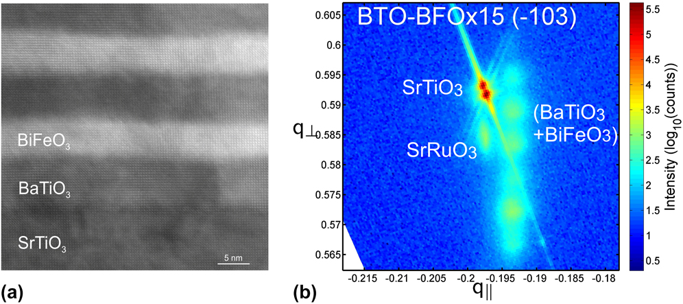
Figure 1(b) highlights the XRD RSM around the asymmetric
 $\left( {\bar 103} \right)$
substrate peak of a multiferroic (BiFeO3/BaTiO3) × 15 superlattice on SrRuO3/SrTiO3(001). The samples represented in Figs. 1(a) and 1(b) were grown simultaneously in a single PLD process. A RSM is a two-axis XRD scan with one axis being a normal ω-2θ-scan (or 2θ-ω), and the other axis being ω. These original scan axis are usually converted into reciprocal lattice units q
⊥ and q
‖, see Fig. 1(b). With that, the position and broadening of the reflections in the RSM yield information on lattice constants, strain, mosaicity, coherence lengths, and lattice match. As visible from the good vertical alignment of the SrRuO3 film and the strong substrate peak in the RSM, the several 10 nm thin SrRuO3 buffer layer grew in-plane lattice matched to the SrTiO3(001) substrate. In contrast, the superlattice peak and the corresponding fringe peaks are not aligned vertically to the substrate peak. The fact that, unlike the SrRuO3 film, the multilayer superlattice exhibits no in-plane lattice matching to the SrTiO3 substrate, but nevertheless interfacial coherence within the multilayer, is quite noteworthy. Again, HR-TEM imaging proves that the interfaces within the superlattice are coherent [see Fig. 1(a)], which is consistent with the results reported in our previous work.
Reference Lorenz, Lazenka, Schwinkendorf, Van Bael, Vantomme, Temst, Grundmann and Höche13
The lattice constant of the used cubic SrTiO3 single crystal substrates was determined to be 0.3906 or 0.3912 nm, depending on the calculation of the lattice constants from the SrTiO3(004) peak of XRD wide angle scans, or the SrTiO3(002) peak of RSMs around (002), respectively. Reference Lorenz, Lazenka, Schwinkendorf, Van Bael, Vantomme, Temst, Grundmann and Höche13 Usually, higher order peaks yield more precise lattice constants, due to reduced XRD goniometer errors. The lattice constant of cubic SrRuO3 is very close to that of SrTiO3, i.e., 0.391 nm, according to, JCPDS (1998) PCPDFWIN v. 2.00, No. 80-1529.
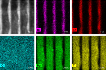
Figure 2 is a high-resolution STEM-EDX map of the main elements of four double layers of a BiFeO3/BaTiO3 superlattice. As visible from the HAADF image and the EDX maps of the cations, the thickness of the nominally 5 nm thick BiFeO3 layer varies in this particular part of the superlattice from 2 nm to about 6 nm. Remarkably, interfacial coherence is retained in spite of the obvious interface roughness, for details see Ref. Reference Lorenz, Hirsch, Patzig, Höche, Hohenberger, Hochmuth, Lazenka, Temst and Grundmann36. The interfacial roughness stems from an insufficient number of pulses to generate an integer number of monolayers, which leads to a restructuring of the surface (during the relaxation time between the BTO and BFO pulse packets). As can be seen in Ref. Reference Lorenz, Lazenka, Schwinkendorf, Van Bael, Vantomme, Temst, Grundmann and Höche13, this growth mode can be easily suppressed, mirroring the two-dimensional growth mode in the interface topography.
STEM-EDX images taken from a thin cross section of a (BiFeO3/BaTiO3) × 15 superlattice on SrTiO3(001), with nominal BaTiO3 and BiFeO3 single film thicknesses of 5 and 10 nm, respectively. The HAADF micrograph (top left) shows a detailed view of the microstructure of three layer pairs within the stack, and the corresponding EDX element distribution maps highlight the lateral distribution of indicated elements within the superlattice.

Furthermore, in the thinner parts of the BiFeO3 layers, also an intermixing with the BaTiO3 layer seems apparent. As our previous work on composite BTO–BFO-films suggests, such an intermixing could be of advantage, however. The intermixing may have impact on the ferroelectric performance of the whole superlattice, and with that, on its magnetoelectric performance. Indeed, this particular superlattice sample showed the highest magnetoelectric voltage coefficient among all our up to now grown (BiFeO3/BaTiO3) × 15 superlattices. A more detailed discussion on elemental distributions and possible chemical intermixing effects in multiferroic superlattices is currently in preparation.
B. Dielectric-plasmonic magnesium oxide–titanium nitride superlattices
Dielectric-plasmonic superlattices of the type TiN–MgO with a periodicity of few nanometers are expected to exhibit a hyperbolic dispersion at visible optical wavelengths. Reference Naik, Schroeder, Ni, Kildishev, Sands and Boltasseva37 It was shown theoretically by Salandrino et al. that planar periodic structures of metals and dielectrics, so-called anisotropic metamaterials, show a hyperbolic dispersion. Reference Salandrino and Engheta38 Possible applications of this effect in optics include, e.g., far-field imaging systems that allow for a resolution below the diffraction limit, i.e., which show subwavelength-resolution. Reference Salandrino and Engheta38
Experimentally, TiN and Al0.72Sc0.28N alternating layers of equal thickness were epitaxially grown on MgO(001) substrates. Reference Naik, Saha, Liu, Saber, Stach, Irudayaraj, Sands, Shalaev and Boltasseva39 Such an TiN–Al0.72Sc0.28N superlattice with TiN as the plasmonic component shows for example a high broadband photonic density of states. Reference Naik, Saha, Liu, Saber, Stach, Irudayaraj, Sands, Shalaev and Boltasseva39 This may be interesting for quantum plasmonic applications in the visible optical range. Reference Naik, Saha, Liu, Saber, Stach, Irudayaraj, Sands, Shalaev and Boltasseva39
As a first step of our work, the layer-by-layer growth of TiN thin films by PLD on in situ annealed (001) MgO was demonstrated recently.
Reference Bonholzer, Lorenz and Grundmann33
Based on these findings, structures with up to ten double layers TiN–MgO were subsequently grown. Figure 3 shows an XRD 2θ-ω scan around the MgO(002) substrate peak, and the RSM around the asymmetric MgO
 $\left( {4\bar 22} \right)$
peak. As demonstration of the superior structural quality of the superlattice, not only the MgO substrate peaks, but also the superlattice peaks and all their satellites show the Kα1/2 splitting of the primary X-rays. This means, the broadening of the film peaks is surprisingly low. The point-like superlattice reflections in the RSM show additionally a low strain gradient and low mosaicity in the TiN–MgO superlattice.
(a) XRD 2θ-ω-scan with strong MgO(002) substrate peak and superlattice satellite peaks. All peaks are splitted due to the used Cu Kα1/2 radiation (b) RSM around the asymmetric MgO
 $\left( {4\bar 22} \right)$
peak indicates a strong substrate peak and superlattice peak, as well as its satellite peaks. All peaks are vertically aligned, which indicates in-plane lattice matching of the superlattice to the substrate.
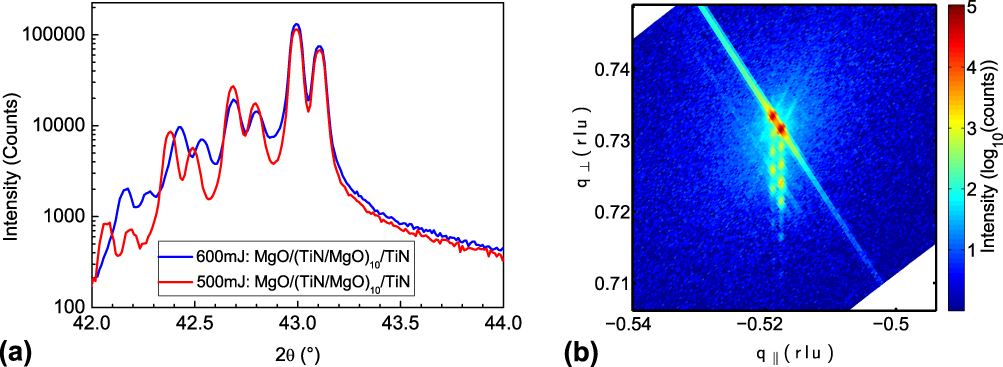
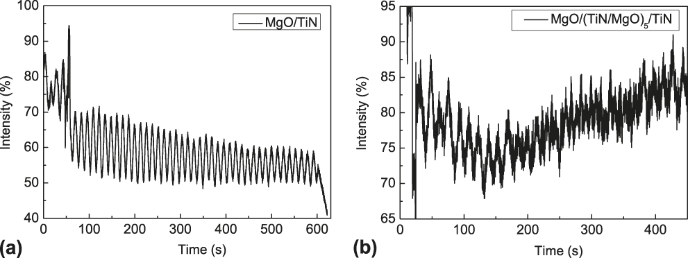
Figure 4 shows RHEED intensity oscillations during growth of the first double layer (a) and the fifth double layer (b) of a TiN–MgO superlattice. This is a demonstration of the persistent layer-by-layer growth of the TiN–MgO superlattice system on MgO(001) up to large total thicknesses of about 100 nm.
RHEED oscillations are observable from (a) the first up to (b) the fifth period of a TiN–MgO superlattice during PLD growth, as indication for the persistent 2D layer-by-layer, i.e., Frank–van-der-Merwe growth.

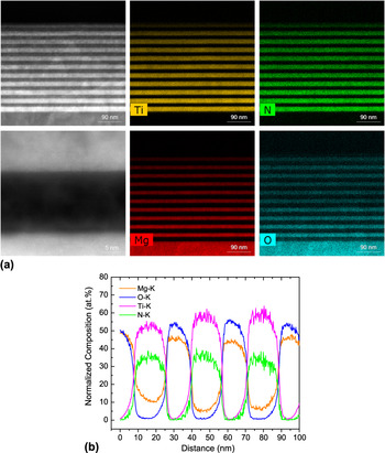
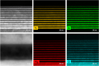
Figure 5 depicts recent STEM-EDX results of a selected TiN–MgO superlattice including a linescan along the first three double layers at the substrate. According to the normalized EDX-linescan, there are indications for minor interdiffusion effects, for example of Mg into TiN. This can be seen in the linescan in Fig. 5(b), where the interfaces between the TiN layers and MgO layers seem less sharp if the distributions of the elements, according to the EDX signal intensities, are compared with the distinct interfaces that are visible in the HAADF micrographs in Fig. 5(a). Especially for Mg, it is observed that the element content within TiN is not zero, even in the center of the TiN layers, at some distance from the inter-layer interfaces. This is different from the other elements, since the O content quickly diminishes to a zero level within TiN at some distance away from the interface, just as, vice versa, the contents of Ti and N within the MgO layers do. Nevertheless, it has to be kept in mind that the lateral resolution of EDX is less good than the STEM-HAADF resolution as such, and possible stray effects, e.g., of the MgO substrate, cannot be excluded completely. However, overall smooth layer interfaces, and homogeneous single layer thicknesses are evident. The EDX maps of Ti, N, and Mg, O clearly indicate the separation of the nitride from the oxide layer, and with that the possibility to grow nitride and oxide layers subsequently in one deposition chamber.
(a) STEM-EDX maps of a typical TiN–MgO superlattice, with high-angle annular dark field (HAADF) micrographs (left grey-scale images), and EDX maps of the indicated elements. All images show smooth interfaces and nearly homogeneous layer thicknesses. The bottom left HAADF image in high-resolution shows the atomic positions and the coherent interfaces near the surface of the superlattice (enlarge view for better visibility). The brighter areas belong to the TiN layers, the dark area is the MgO layer. (b) Normalized EDX linescan of the indicated elements along the first three TiN–MgO double layers beginning at the MgO(001) substrate surface (located at around 0–5 nm at the distance scale). According to this scan, there are indications for minor interdiffusion of Mg into the TiN layers. The data in (a) and (b) are taken from one and the same cross section sample.

C. LaNiO3- and LaMnO3-based superlattices
With increasing technical advance in atomic-scale control of the PLD growth of artificial oxide superstructures, we studied two-dimensional layer-by-layer growth of three kinds of LaNiO3-containing superlattices during the last four years.
At first, we investigated the (001)-oriented LaNiO3/LaAlO3 superlattice, for which density functional theory modeling predicts a superconducting phase. Reference Hansmann, Yang, Toschi, Khaliullin, Andersen and Held23 Temperature-dependent electrical resistivity measurements revealed a metal-insulator transition when lowering the dimensionality of LaNiO3 in the superlattice. By a decrease of the LaNiO3 thickness down to three unit cells, i.e., from three dimensions to two dimensions, the resistivity increased by six orders of magnitude. Reference Wei, Jenderka, Bonholzer, Grundmann and Lorenz26
The second type of superlattice is (111)-oriented LaNiO3/LaAlO3, which was predicted as a topological insulator. Reference Doennig, Pickett and Pentcheva24 The electrical conductivity depends on the polarity-match to the substrate. The intrinsic conductivity mechanisms were discussed by means of appropriate modeling. Reference Wei, Grundmann and Lorenz27 Finally, we investigated LaNiO3/LaMnO3 superlattices, in which an unexpected magnetic exchange bias effect was observed. Reference Wei, Barzola-Quiquia, Yang, Patzig, Höche, Esquinazi, Grundmann and Lorenz28 Since the properties of the above-mentioned superlattices depend highly on the crystalline sample quality, we carefully checked the structural quality of each sample by means of AFM, XRD, and XRR, as shown in the following:
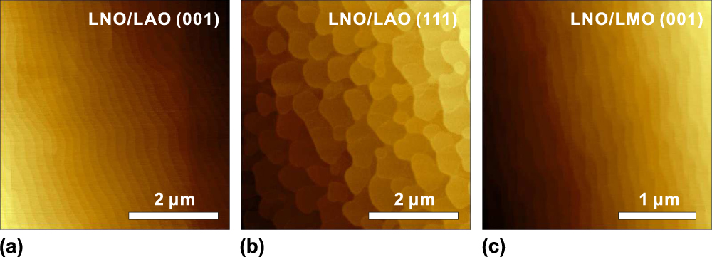
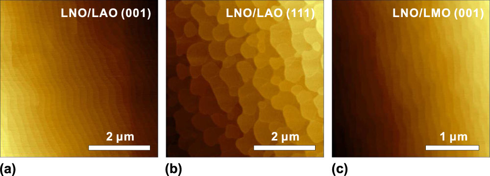
In Fig. 6, the surface morphology of PLD-grown LaNiO3/LaAlO3 and LaNiO3/LaMnO3 superlattices is depicted by means of AFM micrographs. All samples exhibit an atomically flat, terraced surface with root mean square roughnesses below 0.4 nm. The step heights are 0.39 and 0.22 nm for (001)- and (111)-oriented superlattices, respectively, corresponding to one unit cell along these orientations.
AFM images of monolayer terraces taken at the surface of the following superlattice systems: (a) (001)-oriented LaNiO3/LaAlO3 superlattice on SrTiO3(001) substrate. The structure is 6 periods of (4 unit cells LaNiO3 + 2 unit cells LaAlO3), in the following written shortly as [4/2]6. (b) (111)-oriented LaNiO3/LaAlO3 superlattice on a SrTiO3:Nb(111) substrate. The structure of this sample corresponds to [2/2]6. (c) (001)-oriented LaNiO3/LaMnO3 superlattice on a SrTiO3(001) substrate. The structure corresponds to [4/2]6.
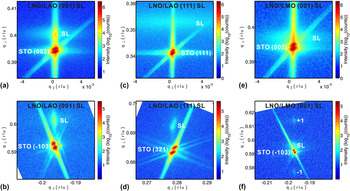
Furthermore, the out-of-plane orientations and in-plane lattice match of the superlattices and corresponding substrates are analyzed by XRD RSMs in Fig. 7. The superlattices show (001) and (111) out-of-plane crystallographic orientations, which is visible from the reflections around the symmetric substrate peaks of (002) and (111), respectively. The perfect in-plane lattice match becomes evident for all samples when considering the vertical alignment of the asymmetric superlattice and substrate peaks as shown in Figs. 7(b), 7(d), and 7(f), respectively. The average thickness of one double layer, i.e., the superlattice period, can be calculated from the distance between adjacent satellite peaks, in very good agreement with TEM data. Giving the example of the LaNiO3/LaMnO3 superlattice, as shown in Fig. 7(f), the thickness of one double layer is calculated to be 2.2 nm, in very good agreement with the nominal design of a [8/2]10 structure, i.e., 10 periods of (8 unit cells LaNiO3 + 2 unit cells LaMnO3), which was controlled by the number of applied laser pulses in PLD.
XRD RSMs around the indicated substrate reflections of the following superlattice samples: (a, b) LaNiO3/LaAlO3 SL on SrTiO3(001) substrate. The corresponding structure is [5/5]10. (c, d) LaNiO3/LaAlO3 SL on SrTiO3(111) substrate. The corresponding structure is [5/5]10. (e, f) LaNiO3/LaMnO3 SL on SrTiO3(001) substrate. The corresponding structure is [8/2]10. (e, f) are adapted from Ref. Reference Wei, Barzola-Quiquia, Yang, Patzig, Höche, Esquinazi, Grundmann and Lorenz28.

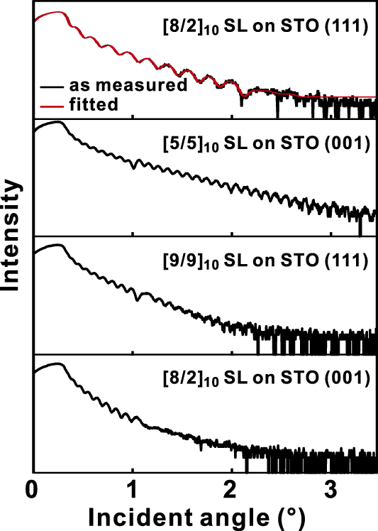
Figure 8 shows a comparison of XRR patterns of various LaNiO3/LaMnO3 superlattices with geometrical configuration as indicated. By modeling of the experimental XRR curves, it was possible to precisely extract the SL structure, thickness, and interfacial roughness.
X-ray reflectivity patterns of the following LaNiO3/LaMnO3 superlattices, demonstrating a very good surface and interface quality: For the top XRR pattern, the designed structure is [8/2]10. The fitted average thicknesses of LaNiO3 and LaMnO3 layers are 1.72 and 0.43 nm, corresponding to 7.9 and 2.0 unit cells, respectively. Along the [111] direction, one unit cell is around 0.218 nm, along the [001] direction, it is 0.384 nm. The fitted interface roughness is around 0.51 nm.
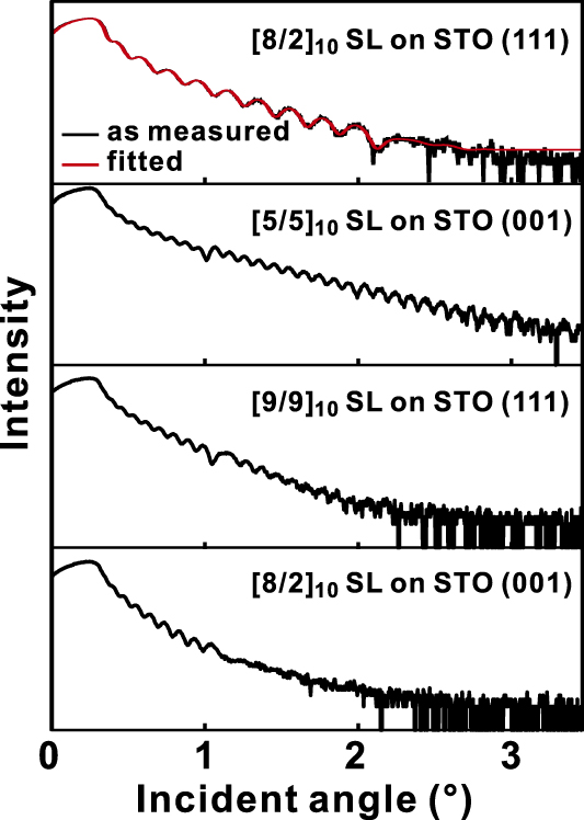
The clearly resolved strong oscillations, which arise from the finite layer thickness, indicate laterally homogeneous samples with abrupt interfaces. For example, the fit to the top XRR pattern results in average thicknesses of the single LaNiO3 and LaMnO3 layers of 1.72 and 0.43 nm, respectively. This is again in very good agreement with our design of 8 LaNiO3 and 2 LaMnO3 unit cells.
In addition, the interfacial roughness obtained from XRR fitting is around 0.51 nm. Compared to published reports, such as for example Refs. Reference Boris, Matiks, Benckiser, Frano, Popovich, Hinkov, Wochner, Colin, Detemple, Malik, Bernhard, Prokscha, Suter, Salman, Morenzoni, Cristiani, Habermeier and Keimer40 and Reference Gibert, Zubko, Scherwitzl, Íñiguez and Triscone41 the interface quality of all our SLs corresponds to the state-of the art.
Since high-quality superlattices were obtained with our growth approach, interesting electronic and magnetic properties could be presented. Reference Wei, Jenderka, Bonholzer, Grundmann and Lorenz26–Reference Wei, Barzola-Quiquia, Yang, Patzig, Höche, Esquinazi, Grundmann and Lorenz28
IV. CONCLUSIONS
In this paper, we present results on the coherent layer-by-layer growth of selected oxide–oxide and oxide–nitride superlattices. In particular, the highest magnetoelectric voltage coefficients in multiferroic (BiFeO3/BaTiO3) × 15 superlattices on SrTiO3(001) were found for samples with low oxygen deficiency, low density of structural defects, and coherent interfaces. This supports the assumption that interfacial strain coupling of the ferroelectric and the multiferroic/magnetic phase is the dominating magnetoelectric coupling mechanism in this kind of superlattices. Furthermore, the superlattice exhibits consistent coherent in-plane lattice matching between the BaTiO3 and BiFeO3 layers independent of lattice matching to the substrate. Since the multiferroic performance of these superlattices depends critically on the interface quality, current efforts aim to improve the growth mode closer toward a more controlled Frank–van-der-Merwe growth.
Dielectric-plasmonic superlattices as combination of the insulating oxide MgO and the metallically conducting nitride TiN with a periodicity of few nanometers are expected to exhibit a hyperbolic dispersion at visible optical wavelengths. We succeeded in growth of TiN–MgO superlattices on MgO(001) via in situ RHEED controlled PLD and observed RHEED oscillations up to five periods TiN–MgO, i.e., clearly confirmed layer-by-layer growth. STEM-EDX maps confirm a clear chemical separation of the nitride layers from the oxides. Spectroscopic ellipsometry investigations are in progress to investigate the optical performance of the oxide–nitride superlattices.
Regarding the LaNiO3- and LaMnO3-based superlattices, we fabricated high-quality perovskite-type thin film heterostructures based on the two-dimensional Frank–van-der-Merwe growth. We found a dimensionality-controlled metal-insulator transition in (001)-oriented LaNiO3–LaAlO3 superlattices. Reference Wei, Jenderka, Bonholzer, Grundmann and Lorenz26 For the (111)-oriented LaNiO3–LaAlO3 superlattices, a polarity-controlled conductivity was observed. Reference Wei, Grundmann and Lorenz27 In LaNiO3–LaMnO3 superlattices, we observed magnetic exchange bias for both (001)- and (111)-oriented samples, in partial contradiction to previously published experiments. Reference Wei, Barzola-Quiquia, Yang, Patzig, Höche, Esquinazi, Grundmann and Lorenz28
Most important, our results highlight once more the potential of two-dimensional Frank–van-der-Merwe growth for fabrication of superlattices with designed functionalities. Based on our results, we can furthermore study other kinds of perovskite-type superlattices with interesting theoretically predicted quantum states.
ACKNOWLEDGMENTS
We thank Gabriele Ramm and Monika Hahn for PLD target preparation, and single crystal substrate preparation, respectively. We kindly acknowledge the financial support from the Deutsche Forschungsgemeinschaft within SFB 762 “Functionality of Oxide Interfaces”.