I. INTRODUCTION
As the portable electronic device, artificial intelligence, and IoT (Internet of Things) markets rapidly expand, so does the demand for nonvolatile memory. Flash memory technology, which is currently being used the most for nonvolatile memory applications, has faced physical limitations and downscaling issues. Therefore, many alternative nonvolatile memory technologies have been investigated such as phase-change RAM (PRAM), ferroelectric RAM (FeRAM), and resistance RAM (RRAM). Reference Kryder and Kim1 Among next-generation nonvolatile memories, PRAM has been considered the most promising candidate due to its high scalability, cost-effectiveness, good compatibility with CMOS technologies, good endurance, and nonvolatility. Reference Simpson, Krbal, Fons, Kolobov, Tominaga, Uruga and Tanida2–Reference Loke, Lee, Wang, Shi, Zhao, Yeo, Chong and Elliott8 The principle of PRAM operation relies on the difference between the electrical resistances of the amorphous and crystalline states, which represent the logic states ‘1’ and ‘0’, respectively. Reference Lai and Lowrey9 Currently, PRAM uses an electrical pulse to melt the phase-change material by joule heating for a RESET operation. Therefore, high power consumption is a major obstacle to developing high-density PRAM. Reference Takaura, Ohyanagi, Tai, Kitamura, Kinoshita, Akita, Morikawa, Kato, Araidai, Kamiya, Yamamoto and Shiraishi10 However, Ge2Sb2Te5, which is the most common phase-change material used in PRAM, requires a high reset current. Because this material has a high melting temperature and low crystalline resistivity, Reference Hosaka, Tamura, Sone and Koyanagi11,Reference Maimon, Hunt, Burcin and Rodgers12 various strategies have been investigated to reduce the reset current, such as structural and material modifications. In the literature, Sb-rich alloys are considered to exhibit growth-dominated crystallization behavior, which could guarantee fast operation speed. Therefore, Sb-rich GeSb phase-change materials have been investigated, but their high reset current and low thermal stability are obstacles that must be overcome to be used in PRAM. In this paper, we chose Se and Ge10Sb90 as the dopant and phase-change material, respectively, because Ge10Sb90 exhibits a fast phase transformation. The Te-doped GeSb alloys have been extensively studied and reported previously. Reference Van Pieterson, Lankhrst, Van Schijndel, Kuiper and Roosen13–Reference Rauox, Cheng, Sandrini, Li and Jordan-Sweet15 Even though Se is just above Te in the same column of the periodic table (i.e., chalcogenides), the melting temperature of Se (T m = 221 °C) is lower than that of Te (T m = 449 °C), and the Ge–Se bond enthalpy (235 kJ/mol) is higher than that of Ge–Te (157 kJ/mol). Since a lower melting temperature enables the use of a lower reset current, and a higher bond enthalpy can improve the thermal stability, we expect that Se doping would be more advantageous for the low-power and high-reliability memory devices than the Te doping reported in previous studies. Furthermore, according to previous reports, both the resistance and crystallization temperature of this system increase with increased Se concentration. Reference Kang, Park, Wamwangi, Wang, Steimer, Choi and Wuttig16,Reference Kang, Choi, Wamwangi, Wang, Steimer and Wuttig17 Therefore, PRAM devices constructed with Se-doped Ge10Sb90 films are expected to consume less power and be more thermally stable than device constructed from conventional Ge2Sb2Te5. The concentration of Se in our experiments was limited up to 20 at.%, since the severe volume shrinkage was observed upon crystallization over 20 at.% of the Se concentration. To verify these expected advantages, we investigated the electrical and thermal properties of Se-doped Ge10Sb90 thin films.
II. EXPERIMENTAL SECTION
Se-doped Ge10Sb90 films with a thickness of 100 nm were deposited onto SiO2/Si(100) and quartz substrates by a direct current (DC) magnetron co-sputtering method using Ge10Sb90 and Pure Se targets in an Ar atmosphere. The base pressure was 5.0 × 10⁻⁸ torr, and the working pressure was 1.0 × 10⁻³ torr. The ratio of Ge10Sb90 to Se was varied from 40:1 to 8:1 by separately controlling the sputtering power of the Ge10Sb90 and Se targets. The chemical compositions of the deposited films were determined by X-ray photoelectron spectroscopy (XPS; K-alpha, Thermo Scientific Inc., Waltham, Massachusetts). The crystallization temperature and activation energy were analyzed using a differential scanning calorimeter (DSC; DSC 8000, Perkin Elmer, Waltham, Massachusetts). The crystallization temperature was measured at a heating rate of 10 °C/min, and the activation energy was investigated at four heating rates (5, 10, 15, and 20 °C/min). The electrical resistance of the thin films was measured in situ as a function of temperature at different heating rates (10–30 °C/min) or isothermal holding temperatures slightly below the crystallization temperature, using a typical two-probe method in a vacuum chamber. To determine the band gap of Se x (Ge10Sb90)100−x films, ultraviolet-visible-near-infrared (UV-Vis-NIR) spectrophotometer (UV-Vis, Cary 5000, Agilent, Santa Clara, California) was used on the films deposited on quartz substrates. To evaluate the electrical properties of the PCM cell, A Keysight B1500A semiconductor device analyzer (Keysight Technologies Inc., Santa Rosa, California) with a pulse-generation system was used. The size of the contact hole was 600 nm, and TiN was used as the top electrode and bottom heater. The phase-change material active layer was 100 nm thick, which was based on the Se-doped Ge10Sb90 films, and was deposited between the top electrode and bottom heater. Reversible resistance switching was performed by a SET-RESET pulse and read by a READ pulse.
III. RESULTS AND DISCUSSION
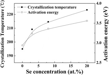
The thermal behaviors of Se-doped Ge10Sb90 films were investigated by DSC at various heating rates. To analyze the crystallization temperature and activation energy, powder samples scratched from thin films of Se-doped Ge10Sb90 were used. Figure 1 shows the crystallization temperature (T c) of the Se-doped Ge10Sb90 films as a function of Se concentration at a heating rate of 10 °C/min. The crystallization temperature increased from 195 to 223 °C as the Se content increased from 0 to 20 at.%. The crystallization temperature is well known to increase with the addition of elements that increase the average bond enthalpy. The type of bonds expected to exist in Se x (Ge10Sb90)100−x films are Ge–Ge (189 kJ/mol), Sb–Sb (126 kJ/mol), Se–Se (206 kJ/mol), Sb–Se (214 kJ/mol), and Ge–Se (235 kJ/mol) bonds. Reference Giridhar, Narasimham and Mahadevan18 A previous report showed that Se atoms tend to bond with different elements, e.g., Ge or Sb, rather other Se atoms, Reference Saleh19 and heteronuclear bonds have larger bond enthalpy than homonuclear bonds. Reference Zachariasen20,Reference Pauling21 Therefore, the increasing concentration of Se can increase the Ge–Se and Sb–Se bond densities, and these bonds have higher bond energies than Ge–Ge and Sb–Sb bonds and can lead to an increase in the average bond enthalpy. Thus, the increase in the average bond enthalpy may reasonably result in a higher crystallization temperature for the phase transition. The Kissinger equation can be used to evaluate the crystallization activation energy. Reference Kissinger22 The linear slope of the Kissinger plot can calculate the crystallization activation energy with four different crystallization temperatures at different heating rates from 5 to 20 °C/min. The crystallization activation energies are shown in Fig. 1. The activation energy for undoped Ge10Sb90 and 20 at.% Se-doped films are 2.94 eV and 3.56 eV, respectively, and this energy increased continuously with the increasing Se concentration. In general, the crystallization activation energy is considered proportional to the average bond enthalpy, which agrees well with the results above. Therefore, the addition of Se can rationally be considered to stabilize the amorphous phase, thus enhancing the thermal stability of PRAM devices.
Crystallization temperature and activation energy as a function of Se concentration in Se-doped Ge10Sb90 films.

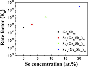
Kinetics analyses of Se-doped Ge10Sb90 films were performed by nonisothermal temperature-resistance measurements. The effective overall reaction rate (K) is determined by the following equation, which is a type of Arrhenius equation, K = K 0 exp(−E a/k b T), where K is the effective overall reaction rate, K 0 is the rate factor, E a is the activation energy, K b is the Boltzmann constant, and T is the temperature. The rate factor is the crystallization kinetic parameter estimated by the Kissinger equation, Reference Kissinger22 i.e., ln[α/T c 2] = C + E a/(k b T), where α is the heating rate. K 0 can be calculated as the exponential of the y-intercept of the fitted line from the Kissinger plot. As shown in Fig. 2, K 0 increased with the increasing concentration of Se. Specifically, the K 0 values of films with Se concentrations of 0, 3, 8, and 20 at.% are 5.25 × 1030, 1.31 × 1031, 1.24 × 1032, and 3.13 × 1033 min−1, respectively. According to previous reports, K 0 is associated with the vibration frequency of an atom, the shape factor during grain growth, and the distance of atomic movement. Reference Chang, Chang, Chang and Chin23,Reference Cheng, Kao, Lee and Chin24 A higher K 0 value may feasibly indicate a high transformation rate. Therefore, PRAM devices made from Se-doped Ge10Sb90 films with high Se concentrations may be able to operate at a faster operation speed than the corresponding films with low Se concentrations.
Rate factor (K 0) of Se-doped Ge10Sb90 films as a function of Se concentration.

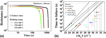
Isothermal crystallization kinetics was used to estimate the thermal stability for PRAM applications. Data retention is one of the important criteria for reliability, and it can be measured by extrapolation from the isothermal Arrhenius plot, which is plotted from the logarithm of the failure time versus 1/k b T. Reference Johnson and Mehl25 The temperatures involved are below the crystallization temperature of Se-doped Ge10Sb90 films, and the failure time is defined as the time required for the resistance to decline to 50% of its original value at the given isothermal temperature, as shown in Fig. 3(a). Figure 3(b) shows the extrapolated temperature corresponding to data retention for a period of ten years (i.e., the ten-year archival life temperature, T 10y) using films with various Se concentrations. In other words, T 10y is the maximum temperature at which data can be retained for ten years, and it increases with the increasing Se concentration. A higher T 10y indicates the enhanced stability of the amorphous phase of the phase-change material, and a material with such stability has a higher crystallization temperature and crystallization activation energy than materials with a low T 10y. The Ge10Sb90, Se3(Ge10Sb90)97, Se8(Ge10Sb90)92, and Se20(Ge10Sb90)80 exhibited T 10y values of 91, 101, 108, 130 °C, respectively, which are all higher than that of Ge2Sb2Te5, namely, 86 °C, as shown in Fig. 3(b). These results indicate that the films with high Se concentrations have better thermal stability than films with low Se concentrations, which is consistent with the results above.
(a) Electrical resistance of Se8(Ge10Sb90)92 film at different isothermal holding temperatures, and (b) Time to failure as a function of reciprocal temperature with various Se concentrations in Se-doped Ge10Sb90 films and Ge2Sb2Te5.

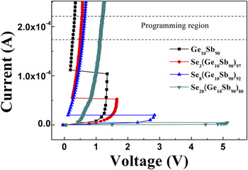
Figure 4 shows the electrical current–voltage (I–V) properties of the PCM device fabricated from Se x (Ge10Sb90)100−x films with various Se concentrations. The I–V measurements were conducted by applying a DC current sweep. The devices using Se-doped Ge10Sb90 films had the same thickness and electrode size. As shown in Fig. 4, the as-deposited films were amorphous in the initial state with high resistance. All the devices switched from the OFF state with high resistance to the ON state with low resistance when the applied voltage exceeded the threshold voltage (V th). The device remained in the low-resistance ON state when the second current sweep was applied. Thus, the I–V curve reveals the typical memory-switching behavior. Reference Lee, Kim, Kim and Kang26,Reference Feng, Zhang, Cai and Chen27 The threshold voltage V th for Se x (Ge10Sb90)100−x films increased from 1.35 to 5.14 V when the Se concentration reached 20 at.%. This may be because Se doping results in increase in the average bond enthalpy and amorphous phase stability. Figure 4 shows the dynamic resistance R d in the programming region. As the Se concentration increased, the dynamic resistance monotonically increased, thus increasing the resistance of the crystalline state film. The R d vale of the Se-doped Ge10Sb90 films increased from 1535 to 5860 Ω with the increasing Se concentration up to 20 at.%. During the writing operation, the dynamic resistance acts as the load resistance. Reference Hwang, Lee, Ahn, Lee, Ryoo, Hong, Koo, Yeung, Oh, Kim, Jeong, Park, Horii, Ha, Yi, Koh, Jeong, Jeong and Kim28 The highest Se concentration yields the highest load resistance, which may signify that a smaller current is required to generate heat. Thus, the power delivery becomes more effective for the writing operation. Therefore, high Se concentrations in Se x (Ge10Sb90)100−x films should lead to a lower writing current than low Se concentrations.
Current versus voltage curves for Se-doped Ge10Sb90 films with various Se concentrations.

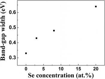
UV-Vis-NIR spectrophotometer analyses were performed to determine the band gap of the Se-doped Ge10Sb90 films. As shown in Fig. 5, the band gap increased from 0.33 eV for the Ge10Sb90 film to 0.64 eV for the Se20(Ge10Sb90)80 film. Thus, Se-doped Ge10Sb90 films with high Se concentrations have a larger band gap than films with less Se. In the literature, the band gap of Se is larger than that of Ge or Sb. Reference Madelung, Rössler and Schulz29,Reference Bhatnagar, Reddy and Srivastava30 The observed increase in the band gap is related to the higher resistance and lower electrical conductivity of the film. Reference Zhou, Wu, Song, Rao, Zhu, Peng, Yao, Song, Liu and Feng31 Generally, electrons cannot move as easily from the valence band to the conduction band when the band gap is larger. Therefore, the increase in band gap with the Se concentration is expected to reduce the operation current and increase the crystallization activation energy, which improves the amorphous phase stability.
Band gap of Se-doped Ge10Sb90 films as a function of Se concentration.

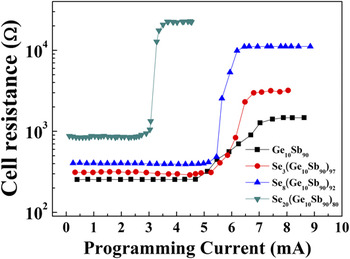
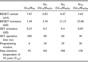
To investigate the resistance–current (R–I) curves of the PCM device employing Se x (Ge10Sb90)100−x films, a RESET pulse was applied to the devices, which was analyzed using a read voltage pulse of 0.2 V. The applied pulse width was 100 ns. Figure 6 shows the resistance as a function of the programming current for several Se concentrations. The resistance of the devices with higher Se contents increased more abruptly with the increasing programming current than that of the devices with less Se. Moreover, both the set (i.e., the crystalline state) and reset (i.e., the amorphous state) resistances of the device increased with the increasing Se concentration. The electrical characteristics of PRAM devices with various Se-doped and undoped Ge10Sb90 films are summarized in Table I. In addition, the set and reset resistances are shown in Table I.
Cell resistance as a function of programming current (i.e., R–I curves) for Se-doped Ge10Sb90 film device with various Se concentrations.

RESET current, RESET resistance, SET resistance, SET operation time, programming window, and maximum ten-year data retention temperature of undoped and Se-doped Ge10Sb90 films.

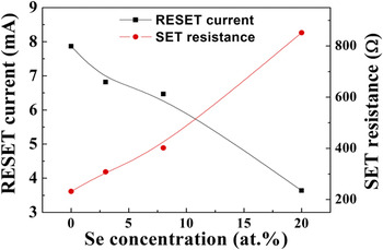
We also analyzed the effect of Se on the reset current and set resistance of Se-doped Ge10Sb90 films. Figure 7 shows the reset current and set resistance as a function of Se concentration. With the increase in the Se concentration from 0 to 20 at.%, the reset current decreases from 7.87 to 3.64 mA (see also Table I), and the set resistance increases from 232 to 852 Ω. These results demonstrate that the reset current is closely related to the set resistance of the Se-doped Ge10Sb90 films because the efficacy of joule heating, which is based on a power law, increases with the increasing resistance of phase-change material. These results indicate that the operation properties of Se-doped Ge10Sb90 films can be enhanced by higher set and reset resistances, which are advantageous for reducing the operation current of memory devices. This is consistent with our above-mentioned results.
Reset current and set resistance variations as a function of Se concentration in Se-doped Ge10Sb90 film devices.

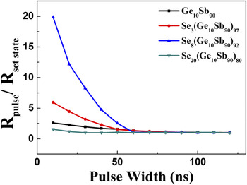
The operation time of PRAM devices is comprised of set and reset operation times. The reset operation time (i.e., the amorphization time) is shorter than the set operation time (i.e., the crystallization time) because full crystallization requires a longer time than amorphization (i.e., the quenching time). Therefore, the set operation time dominates the operation time for the PRAM devices in general. To compare the crystallization speed (i.e., the crystallization time) of the Se-doped Ge10Sb90 films, the R pulse/R set state ratio was measured in the PRAM devices. R pulse is the resistance of the cell under the applied voltage, and R set state is the lowest cell resistance of Se-doped Ge10Sb90 films. When the R pulse/R set state ratio is close to one, the cell is in the set state. Figure 8 shows the R pulse/R set state ratio as a function of the applied pulse width for various Se concentrations. This curve reflects the crystallization speed, and the amplitude of the applied pulse is determined by the voltage that results in the lowest cell resistance for a cell in the reset state. As shown in Fig. 8, the Se-doped Ge10Sb90 films with low Se concentration devices are obviously less crystallized after short pulses than the films with high Se concentration devices. Table I shows the set operation times for all the Ge10Sb90-based devices, which is calculated by the time required to achieve a R pulse/R set state ratio of 0.99. This result means that the PRAM device made from a film with a high Se concentration would have improved operation speed (i.e., a short crystallization time).
Ratio of the resistances reached after applying a pulse to an amorphous cell and the resistance of the SET state, which is plotted versus the width of applied pulse for several Se concentrations.

Table I shows the programming window of all the Se-doped Ge10Sb90 films. The programming window is calculated based on the difference between R set and R reset (measured from Fig. 6), and it increases with the increasing Se concentration from 6 for the undoped Ge10Sb90 film to 26 for Se20(Ge10Sb90)80 film. A larger programming window enables a large signal margin, which can provide a desirable signal-to-noise ratio. Reference Kang, Choi, Wamwangi, Wang, Steimer and Wuttig17 Therefore, we expect that the Se-doped Ge10Sb90 films with a high Se concentration will provide better reliability than the films with a low Se concentration.
IV. CONCLUSION
In this study, we evaluated the thermal and electrical characteristics of Se x (Ge10Sb90)100−x films as a phase-change material by doping elemental Se into Ge10Sb90 films. The crystallization temperature was measured up to 223 °C, and the films with high Se concentrations showed good thermal stability due to the increase in the Se concentration. In addition, the crystallization activation energy and data retention temperature were increased with the increasing Se concentration. The rate factor for undoped Ge10Sb90 and 20 at.% Se-doped films were 5.25 × 1030 and 3.13 × 1033 min−1, respectively. Measurements performed using a UV-Vis-NIR spectrophotometer confirmed that the band gap increases from 0.33 eV for the Ge10Sb90 film to 0.64 eV for the Se20(Ge10Sb90)80 film. It should be noted that the measured activation energy, data retention, rate factor, and band-gap width values are experimental results of the as-deposited materials, not of the melt-quenched materials in the actual devices, which might produce differences in the experimental results. Reference Do, Lee, Sohn, Cho and Ko32,Reference Do, Lee, Bae, Ko, Sohn and Cho33 Therefore, these results should be verified in melt-quenched materials for the application to the actual devices. The electrical performance of Se-doped Ge10Sb90 films was superior to that of the undoped Ge10Sb90 film. The resistance of both the set and reset states of the device increases with the Se concentration. At high Se concentrations, the Se-doped Ge10Sb90 film demonstrated a high threshold voltage and high load resistance. The reset current decreased with the increasing Se concentration. In addition, a faster transition between the amorphous and the crystalline states was observed in the films with higher Se concentration. Finally, the programming window for Se-doped Ge10Sb90 films increased from 6 to 26 from 0 to 20 at.% Se. In summary, the Se20(Ge10Sb90)80 film, which had the highest Se concentration (i.e., 20 at.%), exhibited the highest thermal stability, threshold voltage, largest band gap, ten-year data retention temperature, the highest speed, the lowest power consumption, and the highest reliability of all the films investigated. This could translate into reduced writing currents, improved amorphous phase stability, faster operation speeds, and better reliability. Therefore, Se-doped Ge10Sb90 films are a significantly promising candidate for high-performance PRAM devices.
Supplementary Material
To view supplementary material for this article, please visit https://doi.org/10.1557/jmr.2017.221.
ACKNOWLEDGMENTS
This study was supported by grants from the R&D Program for Industrial Core Technology funded by the Ministry of Trade, Industry, and Energy (MOTIE), Republic of Korea (Grant No. 10039200) and the Joint Program for Samsung Electronics–Yonsei University by Samsung Research Funding Center for Future Technology (SRFC-MA1502-01).