The (Al,Ga,In)N materials system has impacted energy efficiency on the worldwide scale through its application to blue light-emitting diodes (LEDs). This impact on technology and society was recognized by the award of the 2014 Nobel Prize in Physics to Isamu Akasaki, Hiroshi Amano, and Shuji Nakamura. These researchers persevered in their pursuit of this difficult materials system despite the popularity of the competing ZnSe-based system and the widespread scientific opinion that the high dislocation density (>109 cm−2) of III-N films would prevent their application to any useful device.[Reference Nakamura1] The breakthroughs in III-N crystal growth led to the demonstration of high-brightness GaN-based blue and green LEDs by Shuji Nakamura in 1993–1995.[Reference Nakamura, Mukai and Senoh2, Reference Nakamura, Senoh, Iwasa and Nagahama3] After those demonstrations, interest in III-N materials grew rapidly, and the ZnSe system was rendered obsolete for light-emitting applications. Since then, cost reductions and performance improvements have brought GaN-based LEDs into the mainstream, supplanting outdated lighting technology and dramatically improving energy efficiency.
As a result of the increased interest in III-N materials since the early 1990s, not only have blue LEDs improved to the point of widespread commercialization, but also many new properties of the III-N materials system have been identified, explained, and applied to new innovations. The direct, wide band gap of III-N semiconductors makes them promising for solar cell materials[Reference Lang, Neufeld, Hurni, Cruz, Matioli, Mishra and Speck4, Reference Matioli, Neufeld, Iza, Cruz, Al-Heji, Chen, Farrell, Keller, DenBaars, Mishra, Nakamura, Speck and Weisbuch5] intended for ultra-high-efficiency multi-junction stacks. High-frequency GaN electronic devices for power switching applications offer a potential 10% reduction in US electricity demand by replacing entrenched but less efficient silicon technology.[Reference Mishra6] New advances in light-emitting devices have emerged as well, including the expansion of the III-N LED wavelength range to the deep UV[Reference Taniyasu, Kasu and Makimoto7] and the long red spectrum[Reference Ohkawa, Watanabe, Sakamoto, Hirako and Deura8, Reference Kawaguchi, Huang, Wu, Zhao, DenBaars and Nakamura9] and the development of electrically injected III-N quantum well (QW) laser diodes (LDs) emitting in the near-UV[Reference Yoshida, Yamashita, Kuwabara and Kan10] to the green[Reference Takagi, Enya, Kyono, Adachi, Yoshizumi, Sumitomo, Yamanaka, Kumano, Tokuyama, Sumiyoshi, Saga, Ueno, Katayama, Ikegami, Nakamura, Yanashima, Nakajima, Tasai, Naganuma, Fuutagawa, Takiguchi, Hamaguchi and Ikeda11] spectrum. All of these applications have potential in energy efficiency or conversion and are expected to positively impact the energy landscape in the 21st century.
This Prospectives article will focus on just one of these rapidly developing technologies: (Al,Ga,In)N-based QW LDs for long-wavelength applications, primarily blue (440–470 nm), green (515–570 nm), and yellow (570–590 nm) devices. Special attention will be given to non-basal plane (NBP) orientations at these wavelengths. These LDs have near-term applications in displays, projectors, and automotive headlights and long-term applications in general illumination (potentially replacing LEDs), as well as “value added” lighting such as visible light communication (VLC) and smart lighting.
The III-N materials system for LDs in the visible spectrum
The binary nitrides cover a wide range of direct band gap energies with E g = 0.65, 3.4, and 6.0 eV for InN, GaN, and AlN, respectively, which is advantageous for producing a gamut of optoelectronics wavelengths from the IR to the UV spectra. However, the large mismatch in lattice constants between the binary nitrides (Fig. 1) results in highly strained heterostructures with ternary alloys. This strain can lead to defect formation, reduced material quality, and polarization-related electric fields in basal plane growth.
Band gap energy versus lattice constant for III–V and II–VI semiconductors. Open circles indicate indirect band gap materials. InGaN and AlGaN ternary alloys span a large range of lattice constants.

The III-N wurtzite crystal is polar and piezoelectric due to its 6 mm point symmetry. Commercial III-N devices are primarily grown on the basal c-plane (0001) in the polar c-direction by heteroepitaxy on sapphire or SiC substrates. Devices grown on the c-plane offer high performance despite the very high dislocation densities (~109 cm−2) induced by non-native substrates.[Reference Nakamura1] However, c-plane devices also exhibit polarization-induced electric fields in strained heterostructures that bend the energy bands. This results in separation of the electron and hole wavefunctions in strained InxGa1−xN QWs that reduces radiative recombination rates, especially for wide QWs (>3 nm) (Fig. 2). This effect is referred to as the Quantum Confined Stark Effect (QCSE),[Reference Miller, Chemla, Damen, Gossard, Wiegmann, Wood and Burrus12, Reference Takeuchi, Sota, Katsuragawa, Komori, Takeuchi, Amano and Akasaki13] and it is exacerbated by increasing strain associated with increasing indium (In) composition for longer wavelength emitters. As a result, low In content, violet-emitting c-plane QW devices have shown higher efficiencies than longer wavelength devices.[Reference Raring, Hall, Schmidt, Poblenz, Li, Pfister, Feezell, Craig, Speck, DenBaars and Nakamura14]
Simulations of the conduction band (CB), valence band (VB), and electron and hole wavefunctions for LED structures on m-plane ( $1\bar 100$), (
 $20\overline {21} $), and c-plane (0001) orientations. The simulated structure is a single In0.19Ga0.81N QW (width = 6 nm) sandwiched between 10 nm undoped GaN barriers. The QWs and barriers are contained in a p–n junction (N D = 3 × 10¹⁸, N A = 5 × 10¹⁹).
The structure is simulated at room temperature under a 2.7 V bias. The effect of the applied bias and the internal electric fields on the spatial separation of carrier wavefunctions is shown. The surface is to the right.
NBP orientations of the wurtzite (Al,Ga,In)N crystal (Fig. 3) were predicted 15 years ago to eliminate (for nonpolar planes) or reduce (for semipolar planes) the polarization-related electric fields (Fig. 2).[Reference Waltereit, Brandt, Ramsteiner, Trampert, Grahn, Menniger, Reiche, Uecker, Reiche and Ploog15] However, early efforts to perform heteroepitaxy on NBP orientations, for example, a-plane GaN on r-plane sapphire, were unsuccessful due to the high density of extended defects, especially threading dislocations (TDs) and basal plane stacking faults.[Reference Craven, Lim, Wu, Speck and DenBaars16] In 2006, low dislocation density bulk GaN substrates became commercially available and enabled high-quality growth on NBP orientations. This launched a new field of materials research on semipolar and nonpolar surfaces, which has since led to many high-performance and long-wavelength devices.[Reference Kawaguchi, Huang, Wu, Zhao, DenBaars and Nakamura9, Reference Pan, Tanaka, Wu, Zhao, Speck, Nakamura, DenBaars and Feezell17–Reference Enya, Yoshizumi, Kyono, Akita, Ueno, Adachi, Sumitomo, Tokuyama, Ikegami, Katayama and Nakamura19]
The wurtzite crystal structure showing the polar, basal c-plane (0001), nonpolar m-plane ( $1\bar 100$), nonpolar a-plane (
 $\overline {11} 20$), and semipolar planes of interest for blue and green LDs.
New materials or wavelengths for optoelectronic devices are generally developed for LEDs before LDs due to their simpler structure and the fewer requirements for producing spontaneous emission compared with stimulated emission. LED structures typically require one or more QWs sandwiched within a p–n junction. An electron- and/or hole-blocking layer (EBL or HBL) may also be included to reduce carrier overflow and improve efficiency. In addition to these LED layers, LD structures require optical confinement. This is usually achieved for edge-emitting III-N QW LDs with epitaxial InGaN waveguiding and/or AlGaN cladding layers that create a refractive index contrast to confine the optical mode over the gain-producing QWs. Dispersion effects reduce the refractive index contrast for longer wavelength light, so blue and green devices require relatively higher alloy content waveguiding or cladding layers compared with violet devices. The strain associated with these lattice-mismatched heterostructures must be managed, especially for long-wavelength emitters. Alternatively, quaternary AlInGaN cladding layers that are lattice-matched to GaN may be used.[Reference Ueno, Yoshizumi, Enya, Kyono, Adachi, Takagi, Tokuyama, Sumitomo, Sumiyoshi, Saga, Ikegami, Katayama and Nakamura20, Reference Yoshizumi, Adachi, Enya, Kyono, Tokuyama, Sumitomo, Akita, Ikegami, Ueno, Katayama and Nakamura21]
Due to these challenges, direct III-N LDs in the green spectral region (>515 nm) have only been realized in the past 6 years[Reference Raring, Hall, Schmidt, Poblenz, Li, Pfister, Feezell, Craig, Speck, DenBaars and Nakamura14, Reference Yoshizumi, Adachi, Enya, Kyono, Tokuyama, Sumitomo, Akita, Ikegami, Ueno, Katayama and Nakamura21, Reference Miyoshi, Masui, Okada, Yanamoto, Kozaki, Nagahama and Mukai22] and have been demonstrated exclusively on the c-plane and semipolar ( $20\bar 21$) orientations. So far, only spontaneous QW emission has been demonstrated for direct yellow wavelengths, although active research is marching lasing wavelengths steadily upwards.
By contrast, short-wavelength InxGa1−xN QW LDs are already high performing. Violet c-plane LDs with InxGa1−xN (x ≈ 0.10) QWs have been commercialized since the early 2000s for optical data storage in Blu-ray Discs. Blue c-plane QW LDs have also been commercialized and have seen rapid improvements in output power and efficiency in recent years.[Reference Masui, Miyoshi, Yanamoto and Nagahama23] Improvements in LD performance, especially in blue and longer wavelengths, are important for bringing LD sources to general white lighting applications, where they have the potential to increase efficiency, reduce costs, and add value compared with LED sources.
Recently, high-performance, electrically injected green and red LDs have been reported for disc-in-nanowire[Reference Jahangir, Frost, Hazari, Yan, Stark, LaMountain, Millunchick, Ooi and Bhattacharya24, Reference Frost, Jahangir, Stark, Deshpande, Hazari, Zhao, Ooi and Bhattacharya25] and quantum dot[Reference Zhang, Banerjee, Lee, Hinckley and Bhattacharya26, Reference Frost, Banerjee, Sun, Chuang and Bhattacharya27] structures grown by plasma-assisted molecular beam epitaxy. Lower dimensional structures such as these can allow for reduced threshold current densities and increased gain. These structures can also relieve strain, reducing polarization-related electric fields and dislocation densities in III-nitrides to enable higher alloy compositions and longer wavelength emission. Although this review will focus primarily on industry-dominant QW edge-emitting structures, future developments may increase the commercial viability of one-dimensional (1D) and 0D structures.
LDs for solid-state white lighting
Phosphor converted blue LEDs have made dramatic performance improvements over the past 10 years in efficiency and affordability and now provide economic options for many white lighting installations. Their rapid economic payoffs are due to their low electricity consumption and associated operating costs as well as their long lifetimes. One of the main challenges that still limits commercial LEDs, however, is “efficiency droop,” which refers to the reduction in efficiency as the input current density increases.
The droop phenomenon occurs primarily by a mechanism of non-radiative Auger recombination.[Reference Kioupakis, Rinke, Delaney and Van de Walle28, Reference Iveland, Martinelli, Peretti, Speck and Weisbuch29] Auger recombination is a three-particle process and thus is proportional to the cube of the carrier density. In the ABC model,[Reference David and Grundmann30] the internal quantum efficiency (η IQE) of an LED is given by:
 $${\eta _{{\rm IQE}}} = \displaystyle{{B{n^2}} \over {An + B{n^2} + C{n^3}}},$$
where A, B, and C are the Shockley–Read–Hall, radiative, and Auger coefficients, respectively, and n is the carrier density. As such, the Auger recombination term is dominant at high-carrier densities (and high-current densities) where high-power LEDs would operate (J = 100–1000 A/cm2).[Reference David and Grundmann30]
It was previously thought that Auger recombination should be negligible in wide band gap visible nitride LEDs because a limited number of energy- and momentum-conserving direct transitions are available to accept scattered electrons or holes. An indirect mechanism was eventually described in 2011 in which the Auger process is assisted by momentum changes due to phonon interactions and alloy scattering.[Reference Kioupakis, Rinke, Delaney and Van de Walle28] Computational studies showed that this mechanism can predominate for wide band gap materials and that Auger recombination is therefore the primary cause of efficiency droop in III-N LEDs. This was experimentally confirmed by the direct detection of Auger electrons by electroemission spectroscopy in 2013.[Reference Iveland, Martinelli, Peretti, Speck and Weisbuch29]
Currently, c-plane devices use thin QWs (<3 nm), intended to reduce the QCSE. However, the reduced active volume results in exacerbated efficiency droop during operation due to the increased carrier density. As a result, typical blue c-plane LEDs reach their peak internal quantum efficiencies at very low current densities of 1–10 A/cm2. To generate enough lumens, a commercial LED bulb must either contain a small number of LEDs operated at high-power densities (high brightness per chip, reduced efficiency) or many LEDs operated at low-power density (low brightness per chip, near peak efficiency). The former choice incurs the cost of additional heat sinking due to the less efficient chips, and the latter incurs the cost of additional processing and packaging of semiconductor material.
One option for obtaining high efficiencies at high power densities, and thus low cost (high lumens/$), is to use LDs rather than LEDs for the blue photon source. Although the peak wall-plug efficiency for state-of-the-art blue LDs is lower (38%)[Reference Masui, Miyoshi, Yanamoto and Nagahama23] than for blue LEDs (>70%),[Reference Wierer, Tsao and Sizov31] the LD peak efficiency occurs at an input power density (P input ≈ 25 kW/cm2) that is over three orders of magnitude higher than where the LED peak efficiency occurs (P input ≈ 3 W/cm2).[Reference Wierer, Tsao and Sizov31] Thus, the brightness per epitaxial area is tremendously enhanced for LDs.
Improvements to blue III-N LD peak efficiency are expected as the technology develops through research and industry learning, just as LED peak efficiency has improved over the past two decades. The main challenges that currently limit the peak efficiency of III-N blue LDs are the relatively high-threshold current densities (J th ≈ 3 kA/cm2)[Reference Funato, Kim, Ochi, Kaneta, Kawakami, Miyoshi and Nagahama32–Reference Brüninghoff, Eichler, Tautz, Lell, Sabathil, Lutgen and Strauß34] and the low differential efficiencies (η d = 0.5–0.65)[Reference Raring, Schmidt, Poblenz, Chang, Mondry, Li, Iveland, Walters, Krames, Craig, Rudy, Speck, DenBaars and Nakamura33, Reference Pourhashemi, Farrell, Cohen, Speck, DenBaars and Nakamura35, Reference Vierheilig, Eichler, Tautz, Lell, Müller, Kopp, Stojetz, Hager, Brüderl, Avramescu, Lermer, Ristic and Strauss36] caused by high internal optical losses (α i ≈ 15 cm−1)[Reference Melo37] compared with more efficient III–V materials systems (J th < 100 A/cm2,[Reference Michel, Lecomte, Parillaud, Calligaro, Nagle and Krakowski38]η d = 0.88,[Reference Crump, Dong, Grimshaw, Wang, Patterson, Wise, DeFranza, Elim, Zhang, Bougher, Patterson, Das, Bell, Farmer, DeVito and Martinsen39, Reference Li, Chyr, Jin, Reinhardt, Towe, Brown, Nguyen, Berube, Truchan, Hu, Miller, Srinivasan, Crum, Wolak, Bullock, Mott and Harrison40]α i ≈ 1 cm−1[Reference Crump, Dong, Grimshaw, Wang, Patterson, Wise, DeFranza, Elim, Zhang, Bougher, Patterson, Das, Bell, Farmer, DeVito and Martinsen39, Reference Li, Chyr, Jin, Reinhardt, Towe, Brown, Nguyen, Berube, Truchan, Hu, Miller, Srinivasan, Crum, Wolak, Bullock, Mott and Harrison40]). The losses may be mitigated by optimizing the optical confinement to avoid mode overlap with highly absorbing p-type regions, including the p-InGaN waveguiding layer, the p-AlGaN EBL, and/or the p-(Al)GaN cladding layer (Fig. 4). The high optical loss in III-N p-type regions (α matl ~ 100 cm−1) is attributed to phonon-assisted optical absorption by acceptor-bound holes which increases with increasing doping level. Very high Mg p-doping levels ([Mg] > 1019 cm−3) are typically required due to the high acceptor ionization energy (≈200 meV) of the Mg p-dopant.[Reference Kioupakis, Rinke, Schleife, Bechstedt and Walle41]
A schematic of a MQW LD structure that includes both a high refractive index InGaN waveguiding separate confinement heterostructure (SCH) and low refractive index cladding layers made of GaN, AlGaN, or AlInGaN. The p-type layers, including the p-EBL, p-SCH, and p-cladding layers are highly lossy due to the optical absorption associated with high Mg concentrations. The n-side layers are relatively low loss.
A low lasing threshold is important for high efficiency because below threshold, the LD emission is primarily spontaneous, and the efficiency is subject to all modes of non-radiative recombination, including Auger recombination and resulting efficiency droop. The efficiency droops significantly as the LD approaches threshold, but above threshold, all spontaneous and non-radiative recombination rates clamp at their threshold values, allowing the LD efficiency to increase to its peak value.
The low conductivity of the p-doped layers also reduces the LD efficiency by increasing the series resistance. The thick optical confinement layers can have a particularly large contribution to series resistance. Innovative LD designs may enable the removal of some p-doped layers to reduce both internal losses and series resistances. For example, alternative cladding structures such as non-epitaxial transparent conducting oxides,[Reference Hardy, Holder, Feezell, Nakamura, Speck, Cohen and DenBaars42, Reference Chua, Yang, Knollenberg, Teepe, Cheng, Strittmatter, Bour and Johnson43] photonic crystals, air-cladding,[Reference Nedy, Young, Kelchner, Hu, Farrell, Nakamura, DenBaars, Weisbuch and Speck44] or dielectric cladding[Reference Abare, Hansen, Speck, DenBaars and Coldren45] can replace p-side epitaxial cladding. The reduced QCSE for NBP orientations may also allow for epitaxial designs with wide QWs, which can provide enough waveguiding to remove the AlGaN cladding layers completely.[Reference Feezell, Schmidt, Farrell, Kim, Saito, Fujito, Cohen, Speck, DenBaars and Nakamura46] Additionally, NBP orientations have higher barriers to carrier overflow due to their reduced internal electric fields, which may allow for elimination of the highly Mg-doped EBL, especially for long-wavelength emitters which have deep QWs.[Reference Kawaguchi, Huang, Farrell, Zhao, Speck, DenBaars and Nakamura47, Reference Sizov, Bhat, Song, Allen, Paddock, Coleman, Hughes and Zah48]
Recent reviews assessing the viability of III-N LDs to replace LEDs for solid-state lighting suggest the development of NBP orientations to improve projected LD efficiencies.[Reference Wierer, Tsao and Sizov31, Reference Wierer, Tsao and Sizov49] In addition to enabling epitaxial structure variations, NBP orientations can reduce or eliminate QCSE and increase the modal gain. These characteristics are expected to reduce threshold current densities, thus reducing the threshold-clamped values of the A, B, and C recombination rates and improving LD wall-plug efficiency.
Opportunities in NBP orientations for blue LDs
NBP research is relatively nascent, apart from early work on non-native substrates which showed highly defective growth and poor luminescence performance.[Reference Zhao, Farrell, Wu and Speck50] The breakthrough in producing commercial, low TD density, freestanding bulk GaN crystals by hydride vapor phase epitaxy in 2006 opened up this new research arena. Slicing and polishing of c-plane GaN boules now gives researchers access to any desired crystal plane. Some of the highest performing semipolar planes that are now available by this method were not previously accessible on any non-native substrates.[Reference Fujito, Kubo and Fujimura51]
In addition to reduced QCSE, the unbalanced biaxial in-plane stress in NBP QWs separates the top two valence band (VB) energies which leads to anisotropy of the optical gain.[Reference Zhao, Farrell, Wu and Speck50, Reference Domen, Horino, Kuramata and Tanahashi52] The top VB (called the CH1 band[Reference Zhao, Farrell, Wu and Speck50]) has  $\left. {\vert X} \right)$ character [dipole parallel to the [
 $1\bar 210$] for
 $(h0\bar hl)$ planes] and is strongly populated. This leads to polarized emission for NBP LEDs and reduces the VB density of states to enhance gain in NBP LDs.[Reference Zhao, Farrell, Wu and Speck50] NBP LDs with ridges oriented along the high-gain axis should theoretically have higher material gain than c-plane LDs.[Reference Park53] The combination of reduced QCSE and enhanced gain are expected to reduce transparency currents and increase slope efficiency for long-wavelength NBP LDs.[Reference Sizov, Bhat, Wang, Allen, Paddock and Zah54] Additionally, the CH1 band has a smaller hole effective mass than the c-plane VB.[Reference Zhao, Farrell, Wu and Speck50] This increases the hole mobility, possibly leading to more uniform injection into multi-QWs, which has been shown to be a limitation in c-plane structures.[Reference David, Grundmann, Kaeding, Gardner, Mihopoulos and Krames55]
Theoretically, the nonpolar planes should yield the greatest benefit compared with the c-plane due to their complete elimination of internal electric fields and their very high polarization ratios (>95% for m-plane LEDs emitting near 520 nm[Reference Brinkley, Lin, Chakraborty, Pfaff, Cohen, Speck, Nakamura and DenBaars56]), which indicates strong energy splitting of the VBs. For this reason, much early work focused on nonpolar growth on both hetero- and homoepitaxial platforms, particularly on the nonpolar m-plane, which showed several times higher output powers than the nonpolar a-plane in early LED comparisons.[Reference Yamada, Iso, Saito, Hirasawa, Fellows, Masui, Fujito, Speck, DenBaars and Nakamura57] Theoretical calculations predicted that the m-plane would yield higher optical gain than the c-plane or semipolar planes,[Reference Park53] and this is consistent with experimental measurements of the modal gain in commercial LDs using the Hakki–Paoli method.[Reference Melo, Hu, Weisbuch, Schmidt, David, Ellis, Poblenz, Lin, Krames and Raring58]
Despite these advantages, the m-plane has proven challenging for wavelengths longer than violet. Broad electroluminescence peaks are observed in the blue spectrum, attributed to non-uniform In incorporation.[Reference Kelchner, Kuritzky, Fujito, Nakamura, DenBaars and Speck59] New research on miscut m-plane surfaces has yielded improvements to electroluminescence quality in the blue spectrum,[Reference Kelchner, Kuritzky, Nakamura, DenBaars and Speck60, Reference Kuritzky, Myers, Nedy, Kelchner, Nakamura, DenBaars, Weisbuch and Speck61] but access to wavelengths >500 nm is still limited. As the m-plane QW wavelength is increased into the cyan spectrum, a precipitous drop in output power is observed at approximately 490 nm which is concurrent with the formation of a high density of basal plane stacking faults.[Reference Fischer, Wu, Sun, Wei, Huang, Senda, Iida, Iwaya, Amano and Ponce62, Reference Wu, Lin, Chakraborty, Ohta, DenBaars, Nakamura and Speck63] The record longest continuous-wave (CW) lasing wavelength for the m-plane is still 499.8 nm, demonstrated at Rohm Corporation in 2008.[Reference Okamoto, Kashiwagi, Tanaka and Kubota18]
Among the semipolar planes, the most highly researched for blue emission are the ( $11\bar 22$) and the (
 $20\overline {21} $) planes. Co-loaded metalorganic chemical vapor deposition (MOCVD) studies have shown that the (
 $11\bar 22$) plane, inclined 58° from the c-plane, has the highest In incorporation in InGaN layers of any studied plane.[Reference Zhao, Yan, Huang, Huang, Hsu, Tanaka, Pan, Kawaguchi, Fujito, Van de Walle, Speck, DenBaars, Nakamura and Feezell64] This is attractive because in MOCVD, InGaN must be grown at low temperatures in a desorption-limited regime. The In composition of the films is generally adjusted by changing the growth temperature (rather than the In source flow). The (
 $11\bar 22$) plane can tolerate the highest InGaN QW growth temperatures which should, in principle, lead to films with higher crystal quality and lower impurity incorporation.
The primary limitation of the ( $11\bar 22$) plane is its very low Matthews–Blakeslee critical thickness to misfit dislocation (MD) formation which limits blue In0.16Ga0.84N QW thicknesses to approximately 3 nm.[Reference Hsu65] Film thicknesses exceeding the critical thickness for a given In composition form MDs which are strong non-radiative recombination centers.[Reference Hardy, Young, Shan Hsu, Haeger, Koslow, Nakamura, DenBaars and Speck66] Low critical thickness limits the growth of thick InGaN waveguiding layers or AlGaN cladding layers for LD optical confinement. These challenges will be discussed in detail in the “Strain Engineering for Green Emission on Semipolar (Al,Ga,In)N” section.
Unlike the ( $11\bar 22$) plane, which can form natural facets on patterned c-plane regrowth,[Reference Nishizuka, Funato, Kawakami, Fujita, Narukawa and Mukai67] the (
 $20\overline {21} $) plane is completely non-naturally occurring. It is formed commercially by slicing and polishing a c-plane boule at an inclination of 105° from the c-plane. However, MOCVD growth on the (
 $20\overline {21} $) plane has produced smooth morphologies, high wavelength uniformity, high reproducibility, high polarization ratio,[Reference Zhao, Tanaka, Yan, Huang, Chung, Pan, Fujito, Feezell, Van De Walle, Speck, Denbaars and Nakamura68] and higher powers in the blue spectrum than any other NBP. High-performance devices have been achieved, including record low LED droop results using thick QWs (12 nm)[Reference Pan, Tanaka, Wu, Zhao, Speck, Nakamura, DenBaars and Feezell17] and high-performance blue LDs.[Reference Pourhashemi, Farrell, Cohen, Speck, DenBaars and Nakamura35, Reference Megalini, Becerra, Farrell, Pourhashemi, Speck, Nakamura, Denbaars and Cohen69] These qualities make the (
 $20\overline {21} $) plane the biggest competitor to the c-plane for devices in the blue spectrum.
The main limitations for ( $20\overline {21} $) LDs are the difficulty and expense of forming the substrate, the difficulty of forming laser facets, and the restriction of emission to the blue and shorter wavelengths. There exist no naturally occurring cleavage planes for forming facets on (
 $20\overline {21} $) LDs. Thus, laser facets must be formed by dry etching or by dicing and polishing, the former having lower quality, and the latter being more fabrication intensive. The limitation of (
 $20\overline {21} $) emitters to blue and shorter wavelengths derives from the formation of partial dislocations and basal plane stacking faults with high In content (>24%) QWs, similar to what is seen for high In content m-plane QWs.[Reference Wu, Lin, Chakraborty, Ohta, DenBaars, Nakamura and Speck63, Reference Wu, Zhao, Romanov, DenBaars, Nakamura and Speck70]
Strain engineering for green emission on semipolar (Al,Ga,In)N
Until efficient, cost-effective direct green LDs (and LEDs) can be commercialized, white lighting based on LDs (as with LEDs) will continue to use phosphor-conversion systems. These systems generally sacrifice color quality for high efficiency and are ill-suited to provide the color quality needed for laser-based solid-state displays and pico-projectors. These lighting and display applications would ideally operate with red–green–blue (RGB) systems, which have advantages, including higher color quality and “smart lighting,” features which will be discussed later. The green and yellow emission wavelengths are the furthest from widespread commercialization due to the “green gap” phenomenon,[Reference Feezell, Schmidt, DenBaars and Nakamura71] which describes the fall off in efficiency as yellow/green wavelengths are approached from either the long-wavelength (Al,Ga)InP system or the short-wavelength (Al,In)GaN system. The larger energy band offsets between the QWs and barriers for the nitrides compared with the phosphides suggests that better temperature stability and efficiency may be achieved for green/yellow emitters by using nitrides.[Reference Feezell, Schmidt, DenBaars and Nakamura71]
As the In content is increased to >25% for InGaN QWs emitting in the green-to-yellow spectrum, many new challenges arise and existing challenges become exacerbated. The increase in In composition leads to an increase in the compressive strain inside the QW. This causes an increase in the polarization-induced electric fields which lead to more pronounced QCSE, especially for c-plane emitters. Semipolar planes mitigate the QCSE, but the strain in these systems can lead to stress relaxation by the formation of MDs.
Despite the more complicated critical thickness considerations, semipolar technology is expected to make the greatest impact in long-wavelength applications and currently competes with c-plane for direct LDs in the green spectrum. The first direct emission true green (≈525 nm) LD was demonstrated in 2009 on the semipolar ( $20\bar 21$) plane by Enya et al.,[Reference Enya, Yoshizumi, Kyono, Akita, Ueno, Adachi, Sumitomo, Tokuyama, Ikegami, Katayama and Nakamura19] and since then direct green LDs have been demonstrated exclusively on the (
 $20\bar 21$) plane and the c-plane (Fig. 5).
Development of electrically injected QW LDs above 500 nm on the c-plane (circles) and semipolar ( $20\bar 21$) plane (diamonds). Superscripts refer to the following structure types: (1) AlGaN-cladding free, (2) without EBL, (3) topside ITO cladding, (4) LAE.[Reference Takagi, Enya, Kyono, Adachi, Yoshizumi, Sumitomo, Yamanaka, Kumano, Tokuyama, Sumiyoshi, Saga, Ueno, Katayama, Ikegami, Nakamura, Yanashima, Nakajima, Tasai, Naganuma, Fuutagawa, Takiguchi, Hamaguchi and Ikeda11, Reference Raring, Hall, Schmidt, Poblenz, Li, Pfister, Feezell, Craig, Speck, DenBaars and Nakamura14, Reference Okamoto, Kashiwagi, Tanaka and Kubota18–Reference Miyoshi, Masui, Okada, Yanamoto, Kozaki, Nagahama and Mukai22, Reference Raring, Schmidt, Poblenz, Chang, Mondry, Li, Iveland, Walters, Krames, Craig, Rudy, Speck, DenBaars and Nakamura33, Reference Hardy, Holder, Feezell, Nakamura, Speck, Cohen and DenBaars42, Reference Sizov, Bhat, Song, Allen, Paddock, Coleman, Hughes and Zah48, Reference Miyoshi, Masui, Okada, Yanamoto, Kozaki, Nagahama and Mukai72–Reference Masui, Miyoshi, Yanamoto and Nagahama82]
The ( $20\bar 21$) plane, inclined 75° from the c-plane, is a non-naturally occurring growth plane, similar to the (
 $20\overline {21} $) plane, and it also shows remarkably high epitaxial quality. Unlike the (
 $20\overline {21} $) plane, however, the (
 $20\bar 21$) plane does not exhibit basal plane stacking fault formation at high In contents and therefore has been much more successful in producing green devices. Additionally the (
 $20\bar 21$) plane surpasses the c-plane in features such as the homogeneity of In incorporation in the QW and the interface abruptness of epitaxial layers. The effects of its high crystal quality are seen in its narrow EL linewidth and uniform micro-PL.[Reference Takagi, Enya, Kyono, Adachi, Yoshizumi, Sumitomo, Yamanaka, Kumano, Tokuyama, Sumiyoshi, Saga, Ueno, Katayama, Ikegami, Nakamura, Yanashima, Nakajima, Tasai, Naganuma, Fuutagawa, Takiguchi, Hamaguchi and Ikeda11] The performance of (
 $20\bar 21$) devices is also less sensitive than c-plane devices to growth parameters such as ammonia flow and growth rates.[Reference Sizov, Bhat, Wang, Allen, Paddock and Zah54] A limitation of (
 $20\bar 21$) QWs is their much lower polarization ratio than (
 $20\overline {21} $) QWs, despite theoretical predictions that the two planes should have identical degrees of VB splitting.[Reference Zhao, Tanaka, Yan, Huang, Chung, Pan, Fujito, Feezell, Van De Walle, Speck, Denbaars and Nakamura68] This phenomenon is not well understood and experiments on other sets of planes such as the (
 $30\overline {31} $) and (
 $30\bar 31$) planes indeed show similar polarization ratios, as theory predicts.[Reference Zhao, Yan, Feezell, Fujito, Van De Walle, Speck, Denbaars and Nakamura83]
The ( $11\bar 22$) plane has even higher In incorporation than the (
 $20\bar 21$) plane[Reference Zhao, Yan, Huang, Huang, Hsu, Tanaka, Pan, Kawaguchi, Fujito, Van de Walle, Speck, DenBaars, Nakamura and Feezell64] and has shown promising results for green and yellow LEDs.[Reference Feezell, Schmidt, DenBaars and Nakamura71] Its application to long-wavelength LDs, however, is limited because the additional epitaxial layers needed for optical confinement are incompatible with its low critical thickness for MD formation. (AlInGa)N-based blue LDs typically use relatively thick In0.07Ga0.93N waveguiding (≈60 nm) and/or AlGaN/GaN short-period superlattices for cladding to confine the optical mode. Even for these compositions and thicknesses the (
 $11\bar 22$) plane shows evidence of large MD densities.[Reference Hsu, Young, Romanov, Fujito, DenBaars, Nakamura and Speck84]
Stress relaxation via MD formation for semipolar inclinations ≤75°, such as the ( $20\bar 21$) and (
 $11\bar 22$) planes, occurs predominantly by slip on the basal c-plane slip system.[Reference Hsu, Hardy, Young, Romanov, DenBaars, Nakamura and Speck85] In nitrides, this occurs primarily by a mechanism of bend and glide of pre-existing TDs from the substrate.[Reference Hsu, Young, Romanov, Fujito, DenBaars, Nakamura and Speck84] Crystal orientations with higher resolved shear stresses lead to lower critical thickness for MD formation. The higher resolved shear stress on the (
 $11\bar 22$) plane, for example, leads to its lower critical thickness compared with the lower resolved shear stress (
 $20\bar 21$) plane. Relaxation via the basal plane slip system is non-operable for growth on the c-plane or orthogonal a- or m-planes due to the absence of resolved shear stress in these orientations. Thus, only low inclination semipolar planes are subject to this relaxation mechanism.[Reference Hsu, Hardy, Young, Romanov, DenBaars, Nakamura and Speck85]
High inclination planes (>75°), including the ( $30\bar 31$) plane and the m-plane (
 $10\bar 10$), relax predominantly by NBP MDs, including prismatic slip on inclined m-planes.[Reference Hsu, Hardy, Young, Romanov, DenBaars, Nakamura and Speck85] Low inclination planes activate NBP slip as secondary slip systems, and the intersection of BP and NBP MDs can generate new TDs.[Reference Wu, Young, Koslow, Hardy, Hsu, Romanov, Nakamura, DenBaars and Speck86] BP slip leads to 1D arrays of MDs orthogonal to the projected c-direction in the material. Several efforts have been undertaken to prevent the formation of MDs for long-wavelength semipolar LDs, including intentional stress relaxation,[Reference Hsu, Hardy, Wu, Koslow, Young, Romanov, Fujito, Feezell, DenBaars, Speck and Nakamura87] control of dislocation glide through doping,[Reference Hardy, Young, Shan Hsu, Haeger, Koslow, Nakamura, DenBaars and Speck66] and reduction of local MD density through limited area epitaxy.[Reference Hardy, Nakamura, Speck and DenBaars88]
Intentional 1D stress relaxation in the n-side InGaN waveguiding layer can isolate MDs away from the active region. This method was successful in realizing electrically injected lasing wavelengths in blue for ( $11\bar 22$).[Reference Hsu, Hardy, Wu, Koslow, Young, Romanov, Fujito, Feezell, DenBaars, Speck and Nakamura87] As the emission wavelength increases, index dispersion reduces the index contrast between the active and waveguiding/cladding layers and thus reduces the optical confinement. Higher composition waveguiding/cladding layers are usually required to maintain adequate optical confinement. The longest electrically injected wavelength that has been demonstrated for a (
 $11\bar 22$) LD is a 497 nm aquamarine device based on a stress-relaxed buffer layer.[Reference Hsu, Wu, Young, Romanov, Fujito, DenBaars, Speck and Nakamura89] The difficulty in engineering around the low critical thickness and increasing strain for long-wavelength (
 $11\bar 22$) LDs has, so far, limited this plane to LED or short-wavelength LD applications.
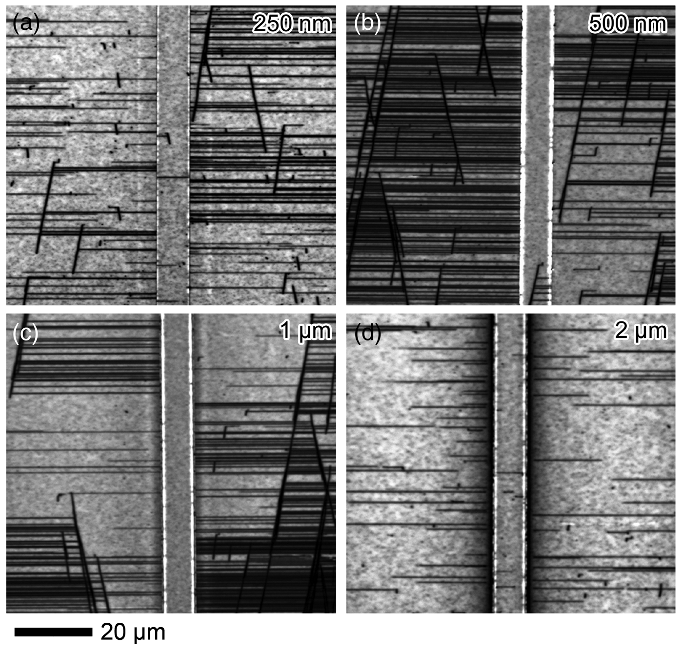
Suppression of MD formation and glide was demonstrated for ( $20\bar 21$) samples by Si and Mg doping of thick waveguiding or cladding layers. The charged impurities (the dopants) may prevent the dislocation motion by surrounding the dislocation core and altering the kinetics.[Reference Hardy, Young, Shan Hsu, Haeger, Koslow, Nakamura, DenBaars and Speck66] Another technique called limited area epitaxy (LAE) has been used to suppress MD stress relaxation by regrowth on substrates with patterned mesas. TD glide stops at the mesa sidewall, limiting the number of MDs on the mesa to the number of pre-existing TDs on the mesa (Fig. 6). This generates highly strained films and allows for a 3× increase in film thicknesses before significant MD formation occurs. LAE opens the design space for waveguiding and cladding layers with increased compositions and thicknesses, therefore increasing the confinement factor for long-wavelength devices.[Reference Hardy, Nakamura, Speck and DenBaars88] Electrically injected green (
 $20\bar 21$) LDs emitting at 523 nm were achieved by the LAE method in 2013 (Fig. 5).[Reference Hardy, Wu, Shan Hsu, Haeger, Nakamura, Speck and DenBaars81]
Cathodoluminescence micrographs of 100 nm In0.08Ga0.92N ( $20\bar 21$) films grown on 5 µm wide LAE stripe mesas parallel to the in-plane projection of the c-plane,
 $[\bar 1104]$, with mesa heights (a) 250 nm, (b) 500 nm, (c) 1 µm, and (d) 2 µm. Glide of MDs formed outside of the mesas is halted at the mesa edge, reducing the MD density on the stripes. (Reprinted with permission from Hardy et al.[Reference Hardy, Wu, Shan Hsu, Haeger, Nakamura, Speck and DenBaars81]. Copyright 2013, AIP Publishing LLC.)
One of the most successful methods for providing optical confinement for long-wavelength LDs while managing strain is the use of quaternary alloy AlInGaN cladding layers.[Reference Takagi, Enya, Kyono, Adachi, Yoshizumi, Sumitomo, Yamanaka, Kumano, Tokuyama, Sumiyoshi, Saga, Ueno, Katayama, Ikegami, Nakamura, Yanashima, Nakajima, Tasai, Naganuma, Fuutagawa, Takiguchi, Hamaguchi and Ikeda11, Reference Enya, Yoshizumi, Kyono, Akita, Ueno, Adachi, Sumitomo, Tokuyama, Ikegami, Katayama and Nakamura19–Reference Yoshizumi, Adachi, Enya, Kyono, Tokuyama, Sumitomo, Akita, Ikegami, Ueno, Katayama and Nakamura21, Reference Adachi, Yoshizumi, Enya, Kyono, Sumitomo, Tokuyama, Takagi, Sumiyoshi, Saga, Ikegami, Ueno, Katayama and Nakamura76, Reference Yanashima, Nakajima, Tasai, Naganuma, Fuutagawa, Takiguchi, Hamaguchi, Ikeda, Enya, Takagi, Adachi, Kyono, Yoshizumi, Sumitomo, Yamanaka, Kumano, Tokuyama, Sumiyoshi, Saga, Ueno, Katayama, Ikegami and Nakamura77] Quaternary layers can be lattice matched to the GaN substrate and still provide adequate index contrast for optical confinement. This method is difficult due to the different optimal MOCVD growth conditions for AlGaN and InGaN; however, Sumitomo Electric and Sony have succeeded in using this epitaxial design to produce the record longest wavelength CW green QW LDs on ( $20\bar 21$) substrates in 2012 (Fig. 5).[Reference Takagi, Enya, Kyono, Adachi, Yoshizumi, Sumitomo, Yamanaka, Kumano, Tokuyama, Sumiyoshi, Saga, Ueno, Katayama, Ikegami, Nakamura, Yanashima, Nakajima, Tasai, Naganuma, Fuutagawa, Takiguchi, Hamaguchi and Ikeda11]
“Value-added” lighting: VLC and smart lighting with III-N LDs
In addition to using LED and LD sources for white lighting, there is an opportunity to leverage the capabilities of these solid-state devices for visible light communication (VLC). The digitization of information has generated increasing demand for online data access via wireless communication systems. It is increasingly common for individuals to download and interact with multiple wireless data streams simultaneously on multiple devices.[Reference Short90]
The high demand for wireless data streaming has led to crowding of Wi-Fi bandwidth, which is transferred through a limited number of radio frequencies. Wireless providers must avoid pre-allocated frequencies already claimed by entities including TV, radio, military, and navigation systems, and there is insufficient bandwidth remaining to provide for the increasing demand. This problem of “spectrum crunch” has driven development of VLC to open up new bandwidth and alleviate the pressure on traditional Wi-Fi systems.
Research into LED-based VLC has gained much traction in the past few years as LEDs have become widely deployed for indoor commercial lighting. VLC requires fast modulation for acceptable data transfer rates. Because LEDs are semiconductor devices, their intensity can be modulated rapidly in response to changes in electrical drive current. This allows for approximately 20 MHz of bandwidth for a typical single LED.[Reference Grubor, Randel, Langer and Walewski91] Smaller area LEDs can be modulated at higher frequencies, which is attributed to their ability to be driven at higher current densities.[Reference Mckendry, Massoubre, Zhang, Rae, Green, Gu, Henderson, Kelly and Dawson92] Techniques including the use of μ-LED arrays (devices <100 µm diameter) for parallel data streams[Reference Mckendry, Massoubre, Zhang, Rae, Green, Gu, Henderson, Kelly and Dawson92] and frequency division multiplexing[Reference Tsonev, Chun, Rajbhandari, McKendry, Videv, Gu, Haji, Watson, Kelly, Faulkner, Dawson, Haas and O'Brien93] have increased the bandwidth to >400 MHz and the data transfer rate into the Gbit/s range.
While LED-based VLC systems are paving the way to commercialization, LDs may offer an even more promising opportunity. The LED modulation frequency is limited by the material carrier lifetime which is of the order of nanoseconds, whereas the LD modulation frequency is limited by the photon lifetime, which is much faster, of the order of picoseconds.[Reference Nakamura, Senoh, Nagahama, Iwasa, Yamada, Matsushita, Sugimoto and Kiyoku94] High modulation speeds have been achieved for InGaN-based LDs including a photodiode-limited speed of 1.4 GHz for a blue-violet LD,[Reference Watson, Tan, Najda, Perlin, Leszczynski, Targowski, Grzanka and Kelly95] and recently, a 2.6 GHz maximum speed for a blue LD measured with a UV-extended high-speed photodiode.[Reference Lee, Zhang, Cantore, Farrell, Oh, Margalith, Speck, Nakamura, Bowers and DenBaars96] If visible lasers are employed for solid-state white lighting, then VLC can be included as a value-added feature to basic room illumination to provide supplementary bandwidth for data download.
If RGB LED or LD systems are used instead of phosphor-conversion systems, greater bandwidth can be achieved as each frequency can be separately modulated and detected by using frequency filters.[Reference Grobe, Paraskevopoulos, Hilt, Schulz, Lassak, Hartlieb, Kottke, Jungnickel and Langer97] The green component in the future may be provided by a high-power semipolar direct LD. An RGB laser system produces a spectrum of narrow wavelength “spikes,” which provide surprisingly good color-rendering. In an experiment comparing illumination of a still-life by a four-color (RGYB) laser source versus phosphor-converted LED sources (warm-white, cool-white, and neutral-white) versus incandescent lights, viewers found the laser light more pleasing than either warm-white or cool-white LEDs and similarly pleasing to the neutral-white LEDs and the incandescent light.[Reference Neumann, Wierer, Davis, Ohno, Brueck and Tsao98] This demonstrates that “spiky spectra” can compete in color quality against the dominant lighting systems.
RGB (or RGYB) luminaries additionally allow for value-added “smart lighting,” such as the ability to dynamically tune color temperatures to the liking of the viewer. They allow for programmable circadian lighting which can be used to reinforce natural circadian rhythms by mimicking the solar spectrum which is reddish (2000 K) in the mornings and evenings and bluish (>6000 K) in the afternoon.[Reference Schubert and Kim99] In 2002, it was discovered that circadian responses are mediated by a photopigment in the eyes called melanopsin.[Reference Berson, Dunn and Takao100, Reference Hattar, Liao, Takao, Berson and Yau101] This photopigment is most sensitive to blue and cyan light (459–484 nm).[Reference Brainard, Sliney, Hanifin, Glickman, Byrne, Greeson, Jasser, Gerner and Rollag102] This and other discoveries suggest future smart lighting applications in therapy for sleep pathologies, including insomnia or jet lag. The symptoms of these pathologies have been shown to improve after exposure of the patient to correctly timed doses of blue-containing light.[Reference Vosko, Colwell and Avidan103]
Value-added lighting systems bring a confluence of many industry players into the lighting market including electric utilities, internet providers, facility management, luminaire designers, and even health care professionals and clinicians. Lighting innovations can improve our quality of life in many ways, including our ability to access rapid data downloads in highly secure light networks, to tune decorative and room lighting to different needs and interests, and to improve our health through light-based therapies. It may be possible to offset the cost of integration of more expensive laser-based systems by providing added value in the overall system, justifying higher-end prices. Thus, value-added laser-based lighting may even be a viable commercial technology in the near future.
LDs based in the III-N materials system are poised for applications in solid-state white lighting due to their wide and direct band gaps and their peak efficiency at high power densities, which could make them competitive with LEDs. NBP LDs have potential advantages over c-plane LDs due to their reduced QCSE and enhanced material gain. However, the lattice mismatch induced by the ternary alloys poses a challenge for blue and longer wavelength LDs, which need high composition waveguiding/cladding layers. Strain engineering techniques, including relaxed buffer layers, doping to suppress dislocation motion, and LAE have been successful in reaching longer wavelength LDs in semipolar structures. LDs grown on the ( $20\bar 21$) semipolar plane using substrate lattice-matched quaternary AlInGaN waveguiding layers have yielded the longest wavelength reported CW green QW LD at 536.6 nm.[Reference Takagi, Enya, Kyono, Adachi, Yoshizumi, Sumitomo, Yamanaka, Kumano, Tokuyama, Sumiyoshi, Saga, Ueno, Katayama, Ikegami, Nakamura, Yanashima, Nakajima, Tasai, Naganuma, Fuutagawa, Takiguchi, Hamaguchi and Ikeda11] Access to direct green wavelengths improves the efficiency of RGB sources, which are immediately applicable to laser-based displays and projectors. If III-N LDs are deployed for laser-based white lighting and combined with value-added services including high-speed VLC or smart lighting, they can be marketed and priced for their full value, which extends far beyond that of the conventional light bulb.
Acknowledgments
We acknowledge funding from the Solid State Lighting and Energy Electronics Center at UCSB. We thank Joseph Nedy for his careful reading of this manuscript and his helpful comments. L. K. acknowledges an NSF Graduate Research Fellowship under Grant No. DGE-1144085.