Introduction
Recently multi-input multi-output (MIMO) antennas have gained popularity owing to their suitable performance in different communication applications. Multi band notched applications [Reference Wu and Xia1–Reference Manohar, Kshetrimayum and Gogoi3], Hyperlan, WiMAX, and WLAN applications [Reference El Bakouchi, Brunet, Razban and Ghammaz4–Reference Khan, Jamaluddin, Aqeel, Nasir, Kazim and Owais6], ISM band applications [Reference Mathialagan7], WiFi and LTE applications [Reference Moradikordalivand, Leow, Rahman, Ebrahimi and Chua8–Reference Zhang and Wang10], GPS/UMTS [Reference Cheng, Chen, Lin and Chen11], GSM, PCS, LTE2300, and 5 G bands [Reference XU, Zhang and Guo12] are some of the possible applications for these antennas. “MIMO” antenna term is dedicated to a technology in which more than one antenna are adopted on both source and destination sides. The adjacency of many antennas in a MIMO system, although yield marvellous outputs, but simultaneously brings about some challenges. The most important of them is the coupling problem. When the antennas work close to each other, the coupling effect between them influences the performance of the others. This in turn deteriorates the antenna overall radiation characteristics. Hence, a suitable solution should be provided to get the most out of MIMO antennas. There has been a vast variety of research studies dedicated for isolation improvement. For instance in [Reference Dai, Li, Wang and Liang13] a compact MIMO antenna is proposed for 2.4 GHz WLAN applications. The high inter-element isolation is obtained by suitable adoption of a defected shorting wall. In this way, better than −20 dB isolation is achieved with a maximum of −43 dB at the central frequency. As another example, the authors in [Reference Ding, Gao, Qu and Yin14] have surveyed a compact broadband MIMO antenna in which the isolation is obtained by locating the constituent antennas orthogonal to each other. This minimizes the coupling and yields a better performance. In [Reference Li, Du, Takahashi, Saito and Ito15] by adding parasitic elements in the MIMO antenna structure, a double-coupling path is introduced which creates a reverse coupling and yields mutual coupling reduction. Although interesting results have been proposed in the literature, but the challenges the MIMO antennas face, still require more attention and discussion. Proposing novel decoupling methods, size miniaturization, and design of novel antenna structures are the topics in this area.
Moreover, it should be kept in mind that in MIMO systems, due to the contribution of many single antennas, almost a bulky volume is needed for the antenna to be installed. Hence, the compactness of the both single and MIMO antennas is an important factor which should be considered in a design process.
In this paper, a two-element MIMO antenna is proposed. The proposed antenna topology is composed of two antennas each of them consists of a simple ground plane on the backside and a combination of L-shaped elements with different lengths on top side. Proper embedment of the conductive elements yields a triple-band operation for the single antenna with focus at WiMAX and WLAN frequency bands. Similarly, the proposed two-element MIMO antenna structure exhibits a triple band operation. Moreover, the adopted simple parasitic element enhances the inter-element isolation significantly. The obtained merits through the proposed structure are summarized as follows:
• Proposing a simple-structured and cost effective single antenna.
• Achieving a triple-band operation through the proposed compact single antenna with focus at in-service frequency bands of WiMAX and WLAN.
• Designing a two-element MIMO antenna with compact dimensions with respect to most of the previously designed two-element MIMO antennas.
• Obtaining a high-isolation level in the MIMO antenna through a simple decoupling element.
This paper is organized in different sections as explained below: In section “Single antenna design and performance”, a single antenna element is proposed and discussed as the constituent element of the MIMO antenna. Then, section “MIMO antenna configuration” introduces the proposed MIMO antenna configuration with two of the aforementioned monopole antennas. In the sequel, in section “MIMO antenna performance analysis”, MIMO antenna performance is discussed in detail. The effect of the embedded slots, the isolating parasitic element, and MIMO antenna performance based on surface current distribution are released in this section. Measured results and their comparison with simulated ones are presented in section “Results and discussion”. Then, with the aim of highlighting the advantages of the proposed MIMO antenna over the similar previous designs, a comparison is established in section “Comparison”. Ultimately section “Conclusion” concludes the paper.
Single antenna design and performance
The proposed single antenna design is shown in Fig. 1. As can be seen, the radiating patch is composed of the combinations of L-shaped elements which are suitably connected to each other. As can be seen the overall size of the antenna is 20 × 20 mm2. A simple rectangular microstrip feed line with length and width of L f = 10.5 mm and W f = 2 mm excites the antenna structure. Moreover, a rectangular ground plane is placed on the backside of the substrate. The antenna with the given values in Table 1 is simulated using finite element method-based high-frequency structure simulator [16] software and the relevant S 11 curve is plotted in Fig. 2. Based on the results in this figure, a triple-band operation with central frequencies of 2.6, 3.7, and 5.2 GHz is obtained for the proposed single antenna. The obtained frequency ranges are in line with WiMAX and WLAN frequency bands. It should be noted that each conductive element plays an important role in the formation of the antenna final performance. Herein, it is seen that three resonances are excited in the S 11 curve. This observation means that there are some elements which influence the surface current distribution at special resonances, yielding a resonance in the antenna S 11 curve. Herein, each resonance is excited by one of the branches in the radiating patch. The governing formula which clarifies the relationship between the excited resonances and antenna structural and physical features is as follows [Reference Deshmukh and Ray17]:
 $$f = \displaystyle{c \over {2L_e\sqrt {\varepsilon _{re}}}} $$
where L e is the electric length of the included conductive elements, and ε re relates to the antenna substrate material. It is clear that suitable placement of conductive elements and proper tuning of their dimensions would yield a desired performance focused on applicable frequency bands.
The proposed single antenna configuration and parameters.

Simulated S 11 curve for the proposed single antenna.

Comparison of proposed MIMO antennas with some of antennas recently reported in papers

Moreover, to investigate the time-domain characteristics of the proposed antenna, the group delay curve is also plotted in Fig. 3. Based on the obtained results, the group delay variation is less than 2 ns which is considered a suitable range for different applications in communication systems.
Simulated group delay for the proposed single antenna.

MIMO antenna configuration
The proposed MIMO antenna is shown in Fig. 4. As mentioned before, the constituent elements are simple monopole antennas discussed in previous section. The total size of the proposed two-element MIMO antenna is 20 × 40 mm2 which is considered a compact structure with easy installation in communication systems and applications. As a well-known fact, when the antennas perform in a close distance from each other, they affect each other. One method to reduce this undesired effect is the embedment of parasitic structures between the antennas. With the aim of isolation enhancement, a T-bar element is included between the monopole antennas on the backside of the substrate. Detailed values of the proposed design are as follows: All the values are in millimeters. W sub = 40 mm, L sub = 20 mm, L g = 4.5 mm, L f = 10.5 mm, W f = 2 mm, W g = 16 mm, W x = 1 mm, L x = L sub, W xx = 5 mm, L 1 = 1.2 mm, L 2 = 1 mm, X 1 = 10 mm, X 2 = 8.2 mm, X 3 = 9 mm, Y 1 = 3.68 mm, Y 2 = 5 mm, Y 3 = 3 mm, and Y 4 = 7 mm.
Configuration of the proposed two-element MIMO antenna.

MIMO antenna performance analysis
To scrutinize the role of L-shaped elements on the MIMO antenna performance, Fig. 5 shows the MIMO antenna design process step by step. As can be seen, in each step, some part of the radiating patch branches is included in the antenna structure to reveal the role of that element in the formation of final performance. The corresponding S 11 curves of the aforementioned four antennas are plotted in Fig. 6. As can be seen, Ant. 1, which includes one L-shaped structure and a microstrip line, covers a band of 4.8 to 6.7 GHz. By adding one other section of the radiating patch in Ant. 2, a dual band operation is observed. The obtained frequency bands are 2.4–3.1 GHz and 5–5.6 GHz. In the third step, the inclusion of all the L-shaped elements, a triple-band operation with central frequencies of 2.7, 3.2, and 5.4 GHz is observed. Finally, in Ant. 4, the T-band parasitic element is included to finalize the antenna topology. As the results indicate, the operating frequency bands are slightly shifted toward higher frequencies. The proposed MIMO antenna operates over three frequency bands. The first obtained bandwidth is 2.15–2.73 with a central frequency of 2.4. The second one is 3.1–3.9, with a central frequency of 3.4, and the third one extends from 5.04 to 6 GHz with a central frequency of 5.4 GHz. The obtained isolation level is more than 20 dB.
The MIMO antenna design process.

S 11 curves for different antennas in the MIMO design process in Fig. 5.

It is worth noting that the above mentioned obtained results are in line with the theoretical governing mathematical formulation as mentioned in (1) in previous sections. The mathematical formula in (1) indicates that as the length of the conductive element increases, the excited frequency shifts toward lower frequencies. In Ant. 1, the excited resonance is around 5.5 GHz. This is while in Ant. 2, where the length of the conductive element on the radiating patch is increased, another resonance is excited at lower frequencies at about 2.7 GHz. In Ant. 3, another L-shaped element is included which is shorter than the conductive elements in Ants. 1 and 2. As it is expected, the excited resonance is between the resonance frequencies excited by Ants. 1 and 2. Obviously, the simulated results are confirmed by the theoretical discussions.
The obtained results regarding the three band operation could be justified by surface current distribution too. Figure 7 shows the surface current distribution on the MIMO antenna at three sample frequencies selected at three operating bandwidths. As can be seen, at 2.4, 3.5, and 5.5 GHz different parts of the radiating patch radiate effectively. These are the elements which contribute at antenna performance at relevant frequency.
Surface current distribution on the proposed MIMO antenna.

To scrutinize the effect of T-bar parasitic element on inter-element isolation, the MIMO antenna configuration with and without the parasitic element is shown in Fig. 8. Corresponding S 11 curves are also plotted in Fig. 9. As can be seen, by the inclusion of the parasitic element, the first and second operating frequency bands are shifted toward lower frequencies. This is while the third bandwidth is widened from the higher edge. Most importantly, the S 21 curve which corresponds to the isolation level is enhanced significantly with the embedment of the parasitic element. This observation is even more dominant over the first and third bands.
MIMO antenna with and without T-bar parasitic element.

MIMO antennas S 11 and S 21 with and without T-bar parasitic element.

Two metrics which are used to discuss how independent the antennas work beside each other, are envelope correlation coefficient (ECC) and total active reflection coefficient (TARC). ECC shows the independency of the antennas radiation patterns. The lower values of ECC correspond to more independency of the antennas. ECC is calculated based on the following formulation:
 $${\rm ECC} = \displaystyle{{{\vert {S_{11}^{^\ast} S_{12} + S_{21}^{^\ast} S_{22}} \vert } ^2} \over {\lpar {1-{\vert {S_{11}} \vert }^2-{\vert {S_{21}} \vert }^2} \rpar \lpar {1-{\vert {S_{22}} \vert }^2-{\vert {S_{12}} \vert }^2} \rpar }}$$
As mentioned, lower values of ECC show higher isolation. The simulated and measured ECC curve for the proposed MIMO antenna is plotted in Fig. 10. As can be seen, in the case of both simulation and measurement, ECC is not more than 0.03 over the entire frequency band in both simulation and measured results. This range confirms the suitable isolation of the constituent antenna elements.
Simulated and measured ECC curve for the proposed MIMO antenna.

Moreover, as the other parameter, TARC is defined as the square root of the ratio of total reflected power to the total incident power and its apparent return loss of the overall MIMO antenna system. In the case of MIMO antenna which comprise two antenna elements, TARC is calculated as follows:
 $${\rm TARC} = \sqrt {\displaystyle{{{(S_{11} + S_{12})}^2 + {(S_{21} + S_{22})}^2} \over 2}} $$
TARC values lower than 0 dB are desired in MIMO systems. Simulated and measured TARC values are depicted in Fig. 11. It is clearly seen that suitable results are obtained in both simulation and measurement.
Simulated and measured TARC curve for the proposed MIMO antenna.

Results and discussion
To assess the validity of the obtained simulated results, a prototype is fabricated and measured in antenna and microwave laboratory. The fabricated prototype which is connected to PNA (EVA368) E8363C for S-parameters measurement is shown in Fig. 12. The simulated and measured S 11 and S 21 performance are shown in Fig. 13. The results indicate that the antenna has a bandwidth (for S 11 < −10 dB) of 2.15–2.73 with a central frequency of 2.4, 3.1–3.9 with a central frequency of 3.5, and 5.04–6 GHz with a central frequency of 5.5 GHz. Moreover, the isolation (in terms of S 21) is below 20 dB at the same frequency band. Simulated and measured results confirm each other.
Fabricated MIMO antenna under measurement process.

Simulated and measured S 11 and S 21 for the proposed MIMO antenna.

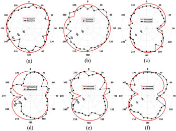
Apart from the S parameters, peak gain and radiation efficiency of the proposed MIMO antenna is also studied in Fig. 14. An efficiency of about 90% with gain values between 2 and 4 dBi is observed for the antenna. As mentioned earlier, group delay of the antenna is an important parameter which should be considered in antenna performance analysis. Figure 15 shows the antenna group delay. It is seen that less than 1.5 ns variation is obtained for the antenna. Antenna radiation patterns at six different frequencies are plotted in Fig. 16. The results confirm the suitability of the radiation patterns in xz and yz planes.
Simulated peak gain and radiation efficiency for the proposed MIMO antenna.

Simulated group delay for the proposed MIMO antenna.

The radiation pattern of the proposed MIMO antenna in (a) 2.4 GHz, (b) 3.5 GHz, (c) 5.5 GHz in the Y–Z plane and (d) 2.4 GHz, (e) 3.5 GHz, and (f) 5.5 GHz in the X–Z plane.

Comparison
To clarify the advantages of proposed design over previously designed similar structures, a comprehensive comparison is carried out. The comparison terms include antenna dimensions, operating frequency bands, and isolation between antennas. Table 1 summarizes the results. The provided data show that the proposed antenna has a compact size. The antennas in [Reference Sharawi, Ikram and Shamim18–Reference Ekrami and Jam23] although having larger sizes which yield more freedom degree but provide less or equal frequency bands as the antenna in this paper. Moreover, the isolation status is better than the antennas in [Reference Sharawi, Ikram and Shamim18–Reference Ekrami and Jam23]. A brief comparison reveals the superior performance of the antenna in this work.
Conclusion
In this article, a very compact structure (20 × 40 mm) is designed and built for portable multifunctional applications. The design is very simple and cost-effective, and the proposed MIMO antenna consists of two antennas with four L-shaped structures in each of the radiation elements and a ground plane for each monopole antenna. Using these L-shaped structures, the MIMO antenna covers the bands 2.15–2.73 with a central frequency of 2.4, 3.1–3.9 with a central frequency of 3.5, and 5.04–6 GHz with a central frequency of 5.5 GHz. In order to increase the isolation between the elements, a T-shaped parasitic structure was placed between the monopole elements to reduce the isolation to below 20 dB. Small size, simple structure, and high isolation are some of the benefits of this designing. In addition, the simulated results and the measurements of are confirmed each other. Eventually, the proposed MIMO antenna can be introduced as a convenient antenna for portable wireless and multi-band applications.
 T. Azarinasab was born in 1986 in Iran. He received the B.Sc. degree in Electrical Engineering from Amol Institute of Higher Education, Amol, Iran. He is currently working toward the M.Sc degree in RF and microwave engineering at Aeen Kamal University, Urmia, Iran.
 Ch. Ghobadi was born in June, 1960 in Iran. He received his B.Sc. in Electrical Engineering Electronics and M.Sc. degrees in Electrical Engineering Telecommunication from Isfahan University of Technology, Isfahan, Iran and Ph.D. degree in Electrical-Telecommunication from University of Bath, Bath, UK in 1998. From 1998 he was an Assistant Professor and now he is a Professor in the Department of Electrical Engineering of Urmia University, Urmia, Iran. His primary research interests are in antenna design, radar, and adoptive filters.
 Burhan Azarm was born in 1992 in Iran. He received the B.Sc. degree in Power Engineering from Islamic Azad University and M.Sc. degrees in Electrical Engineering Telecommunication from Urmia University. He is currently working toward the Ph.D. degree in RF and microwave engineering at Urmia University. His research interests include Antennas, Microwave, and Electromagnetics.
 M. Majidzadeh was born in 1987 in Urmia, Iran. She received her Ph.D., M.Sc. and B.S. degrees in Electrical Engineering from Urmia University in 2016, 2012, and 2009, respectively. Now she is an assistant professor in Department of Electrical and Computer Engineering, Urmia Girls Faculty, West Azarbaijan branch, Technical and Vocational University (TVU), Urmia, Iran. Her research interests are in electromagnetic compatibility, frequency selective surfaces, MIMO antennas, antenna bandwidth enhancement and antenna miniaturization techniques, circularly polarized antennas, and numerical method in electromagnetics.