I. INTRODUCTION
Magnetic resonant wireless power transfer (MRWPT) is currently receiving a significant interest among researchers. In [Reference Costanzo, Dionigi, Mastri, Mongiardo, Russer and Russer1] an extended review of the work published up to 2013 has been presented. Several important contributions [Reference Kurs, Karalis, Moffatt, Joannopoulos, Fisher and Soljacic2–Reference Russer and Russer22], have been reviewed and the interested reader is referred to [Reference Costanzo, Dionigi, Mastri, Mongiardo, Russer and Russer1] for more details. Here we prefer to focus on more recent developments that allow us to deal with the design of wireless power transfer (WPT) links in a systematic way.
Recently, an excellent contribution [Reference Inagaki23] on MRWPT systems has been presented. This approach is based on the conjugate image impedances introduced in [Reference Roberts24]. In particular, the conjugate image parameters, which are an intrinsic property of two-port lossy networks, are the complex reference impedances which allow us to achieve perfect matching at a given frequency. In other important contributions [Reference Bird, Rypkema and Smart25, Reference Zargham and Gulak26], the problem of how to realize load and matching elements in such a way to maximize efficiency have been investigated. Subsequently, in [Reference Dionigi, Mongiardo and Perfetti27], it has been shown the relationship between the solution that maximizes efficiency and the conjugate image impedances. Moreover, it has been pointed out that, in addition to investigate the efficiency of the network, it is also important to consider the amount of power available on the load. In particular, it has been shown that the load that realizes maximum efficiency is different from the load that allows us to maximize the received power.
In [Reference Costanzo, Dionigi, Mastri, Mongiardo, Russer and Russer28] two networks have been introduced that allow us to realize, in addition to the WPT link, also a 1:n transformer. The latter is particularly useful for achieving a sought value of input impedance. In the present work, we illustrate the complete theoretical approach and its application to the two networks presented in [Reference Costanzo, Dionigi, Mastri, Mongiardo, Russer and Russer28].
It is found that for the simple network composed by coupled inductors (and relative matching elements) the values of the load resistance that allows us to realize maximum efficiency or maximum power transfer are different. On the other hand, the reactive matching elements are independent of the coupling and of the quality factors.
On the contrary, for the networks that realize the 1:n transformers, the value of the reactive elements depends on the coupling. However, for the case of maximum power on the load, the value of the load impedance is fixed and does not depend on coupling.
The paper is organized as follows: in Section II we illustrate the general results for the design of matching networks and load selection for a WPT link. The section is divided into two subsections, one illustrating the design for maximum efficiency and the other illustrating the design for maximum power on the load. In Section III, the theory is applied to two cases: the case of coupled inductors and the case of another network configuration that, in addition to performing wireless power transfer, also realizes a 1:n transformer. In Section IV, an example illustrates the application with the realization of a WPT link with 50 Ω input impedance.
II. DESIGN OF MATCHING NETWORKS AND LOAD SELECTION FOR A WPT LINK
A wireless power link between a transmitter and a load can be described as a two-port network; its impedance matrix for a reciprocal network is given by the following equation:
 $$\left[ {\matrix{ {{z_{11}}} & {{z_{12}}} \cr {{z_{21}}} & {{z_{22}}} \cr}} \right] = \left[ {\matrix{ {{r_{11}} + j{x_{11}}} & {{r_{12}} + j{x_{12}}} \cr {{r_{12}} + j{x_{12}}} & {{r_{22}} + j{x_{22}}} \cr}} \right]. $$
As noted in [Reference Roberts24] we can introduce the conjugate image impedances Z
c1, Z
c2 which are defined in the following way. When port 2 is terminated on Z
c2 we see at input port of the two-port network the impedance
 $Z_{c1}^{\ast}$
(here and in the following the asterisk denotes the complex conjugate). Similarly, when port 1 is terminated on Z
c1 we see from port 2 the impedance
 $Z_{c2}^{\ast} $
. Accordingly, the conjugate image impedances must satisfy the equations:
 $$Z_{c1}^{\ast} = {z_{11}} - \displaystyle{{z_{12}^2} \over {{z_{22}} + {Z_{c2}}}}, $$
 $$Z_{c2}^{\ast} = {z_{22}} - \displaystyle{{z_{12}^2} \over {{z_{11}} + {Z_{c1}}}}. $$
It is convenient to introduce the parameters:
 $${\chi \,^2} = \displaystyle{{x_{12}^2} \over {{r_{11}}{r_{22}}}}, $$
 $${\xi \,^2} = \displaystyle{{r_{12}^2} \over {{r_{11}}{r_{22}}}}, $$
and
 $${\theta _r} = \sqrt {(1 - {\xi ^2})(1 + {\chi ^2})}, $$
 $${\theta _x} = \xi \chi. $$
The conjugate image impedances Z ci are given by [Reference Roberts24]:
 $${Z_{c1}} = {R_{c1}} + j{X_{c1}} = {r_{11}}({\theta _r} + j{\theta _x}) - j{x_{11}}, $$
 $${Z_{c2}} = {R_{c2}} + j{X_{c2}} = {r_{22}}({\theta _r} + j{\theta _x}) - j{x_{22}}. $$
A) Maximum efficiency solution
By denoting with P in the input power and with P L the active power dissipated on the load, we can introduce the definition of the efficiency η as
 $$\eta = \displaystyle{{{P_L}} \over {{P_{in}}}}. $$
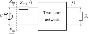
It is possible to show [Reference Dionigi, Mongiardo and Perfetti27] that, with reference to Fig. 1, when we select Z L = Z c2 and Z m1 = jX c1 we achieve the maximum efficiency. By denoting with a prime the quantities that refer to the maximum efficiency solution, we therefore have:
 $${R^{\prime}_L} = {r_{22}}{\theta _r}, $$
 $${X^{\prime}_L} = {r_{22}}{\theta _x} - {x_{22}}, $$
 $${R^{\prime}_{m1}} = 0, $$
 $${X^{\prime}_{m1}} = {r_{11}}{\theta _x} - {x_{11}}. $$
Two-port network with added matching impedance Z m1. We can select the load impedance Z L = R L + jX L and the matching impedance Z m1 to realize either maximum efficiency or maximum power transfer to the load.

By recalling the definition of the conjugate image impedance it is readily found that:
 $${Z^{\prime}_{in}} = {R^{\prime}_{in}} = {R_{c1}} = {r_{11}}{\theta_r}. $$
It is advantageous to introduce the power P 0 defined as
 $${P_0} = \displaystyle{{V_1^2} \over {2{r_{11}}}}, $$
and normalize all the power quantities with respect to P 0. When the conditions (11)–(14) are realized, we have the following expressions for the normalized input power, active power on the load and efficiency:
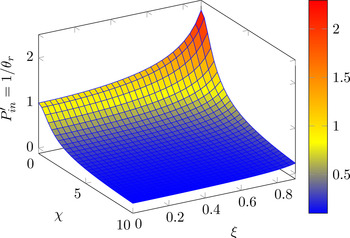
 $${P^{\prime}_{in}} = \displaystyle{1 \over {{\theta_r}}}, $$
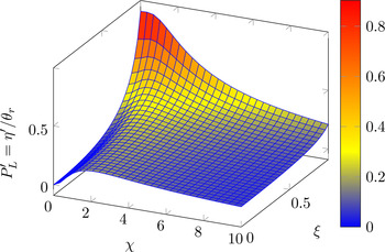
 $${P^{\prime}_L} = \displaystyle{{\eta^{\prime}} \over {{\theta_r}}}, $$
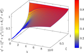
 $$\eta^{\prime} = \displaystyle{{{\xi^2} + {\chi^2}} \over {{{\left( {{\theta_r} + 1} \right)}^2} + \theta_x^2}}. $$
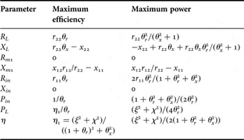
The behavior of input power, output power and efficiency with the parameters χ, ξ for the maximum efficiency solution, i.e. the last three rows of column 2 of Table 1 are illustrated in Figs 2–4, respectively.
Maximum efficiency solution: input power as a function of
 $\chi = {x_{12}}/\sqrt {{r_{11}}{r_{22}}} $
and
 $\xi = {r_{12}}/\sqrt {{r_{11}}{r_{22}}} $
.

Maximum efficiency solution: output power as a function of χ, ξ.

Maximum efficiency solution: efficiency as a function of χ, ξ.

A summary of the parameters’ values for the approaches that maximize efficiency and power. By taking the conjugate matching solution and setting R m1 = 0 we recover the solution with maximum efficiency.

The parameters have the following meanings:
 $\chi = {x_{12}}/\sqrt {{r_{11}}{r_{22}}} $
,
 $\xi = {r_{12}}/\sqrt {{r_{11}}{r_{22}}} $
,
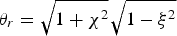 ${\theta _r} = \sqrt {1 + {\chi ^2}} {\kern 1pt} \sqrt {1 - {\xi ^2}} $
,
 ${\theta _x} = \chi \xi $
. The power has been normalized with respect to
 ${P_0} = V_1^2 /(2{r_{11}})$
.
B) Maximum power transfer
The values of the load impedance Z L and of the matching impedance Z m1 which realize the maximum power transfer solution are [Reference Dionigi, Mongiardo and Perfetti27]:
 $${R^{\prime\prime}_L} = {r_{22}}\displaystyle{{\theta _r^2} \over {\theta _x^2 + 1}}, $$
 $${X^{\prime\prime}_L} = - {x_{22}} + {r_{22}}{\theta _x} + {r_{22}}\displaystyle{{{\theta _x}\theta _r^2} \over {1 + \theta _x^2}}, $$
 $${R^{\prime\prime}_{m1}} = 0, $$
 $${X^{\prime\prime}_{m1}} = {r_{11}}{\theta _x} - {x_{11}}. $$
It is noted that the matching impedance Z m1 is purely reactive and equal for the two approaches that maximize efficiency and power. On the contrary, the load resistance is different in the two cases; also the load reactance is in general different for the two cases. By simple network considerations we can obtain the input impedance, input power, power on the load, and efficiency as:
 $${R^{\prime\prime}_{in}} = 2{r_{11}}\displaystyle{{\theta _r^2} \over {1 + \theta _r^2 + \theta _x^2}}, $$
 $${P^{\prime\prime}_{in}} = \displaystyle{{1 + \theta _r^2 + \theta _x^2} \over {2\theta _r^2}}, $$
 $${P^{\prime\prime}_L} = \displaystyle{1 \over 4}\displaystyle{{{\chi ^2} + {\xi ^2}} \over {\theta _r^2}}, $$
 $$\eta^{\prime\prime} = \displaystyle{1 \over 2}\displaystyle{{{\chi ^2} + {\xi ^2}} \over {1 + \theta _r^2 + \theta _x^2}}. $$
For ease of reference all the relevant equations are summarized in Table 1.
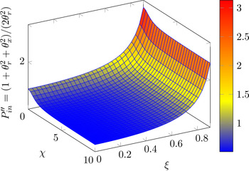
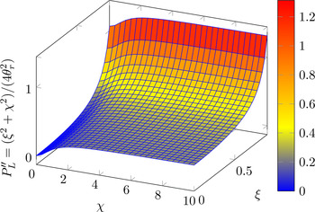
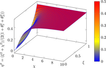
The behavior of input power, output power, and efficiency with the parameters χ, ξ for the solution which maximizes output power, i.e. the last three rows of column 3 of Table 1 are illustrated in Figs 5–7, respectively.
Maximum output power solution: input power as a function of χ, ξ.

Maximum output power solution: output power as a function of χ, ξ.

Maximum output power solution: efficiency as a function of χ, ξ.

We are now in a position to apply the general theory of this section to specific cases. We will start from the simplest case of two coupled inductances and then increase the network complexity in order to illustrate some of the possibilities.
III. APPLICATION TO COUPLED INDUCTORS AND 1:n TRANSFORMERS
A) Coupled inductors
The simplest link is provided by coupled inductors; their impedance matrix is the following:
 $$\left[ {\matrix{ {{z_{11}}} & {{z_{12}}} \cr {{z_{21}}} & {{z_{21}}} \cr}} \right] = \left[ {\matrix{ {{r_1} + j\omega {L_1}} & {j\omega M} \cr {j\omega M} & {{r_2} + j\omega {L_2}} \cr}} \right]. $$
It is convenient to introduce the following parameterization:
 $$\omega = u{\omega _0}, $$
 $${L_1} = \displaystyle{{{X_0}} \over {{\omega _0}}}, $$
 $${L_2} = {L_1}{N^2}, $$
 $$M = {L_1}Nk, $$
 $${r_1} = \displaystyle{{{X_0}} \over {{Q_1}}}, $$
 $${r_2} = \displaystyle{{{X_0}{N^2}} \over {{Q_2}}}. $$
The quantity ω
0 is the angular frequency selected for operating the WPT link; u plays the role of a normalized frequency. The parameter N
2 is the ratio between L
2 and L
1. The mutual coupling M is expressed as usual as
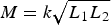 $M = k\sqrt {{L_1}{L_2}} $
, with k representing the coupling coefficient; when a particular configuration is chosen the nominal coupling coefficient for that configuration will be denoted by k
0. The resistances are expressed in terms of the quality factors Q
1 and Q
2. When substituting the equations (29)–(34) into (28) we obtain:
 $$\left[ {\matrix{ {\displaystyle{{{X_0}} \over {{Q_1}}} + j{X_0}} & {j{k_0}{X_0}N} \cr {j{k_0}{X_0}N} & {\displaystyle{{{X_0}{N^2}} \over {{Q_2}}} + j{X_0}{N^2}} \cr}} \right]. $$
It is apparent that since r 12 = 0 we have
 $${\chi ^2} = k_0^2 {Q_1}{Q_2}, $$
 $${\xi ^2} = 0, $$
 $${\theta _r} = \sqrt {1 + {\chi ^2}}, $$
 $${\theta _x} = 0. $$
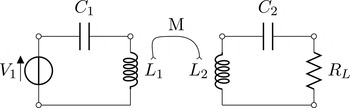
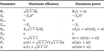
The relevant quantities of interest are summarized in Table 2. It is readily observed that the matching element X
m1 = −X
0 is realized by a capacitance C
1 of value
 ${C_1} = 1/(\omega _0^2 {L_1})$
, as shown in Fig. 8. Similarly, the reactive part of the load impedance X
L
is realized by a capacitance C
2 of value
 ${C_2} = 1/(\omega _0^2 {L_2})$
.
Matching network for coupled inductances. Note that
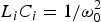 ${L_i}{C_i} = 1/\omega _0^2 $
, i = 1, 2 at the operating angular frequency ω
0. The value of R
L
is provided in Table 2.

A summary of the parameters’ values for the approaches that maximize efficiency and power for coupled inductors.

The parameters have the following meanings:
 ${\chi ^2} = \alpha = k_0^2 {Q_1}{Q_2}$
and R
0 = X
0
N
2/Q
2. Note that the quantities P
in
, PL
, are normalized with respect to
 ${P_0} = V_1^2 /(2{r_{11}})$
. In the present case, we have r
11 = X
0/Q
1.
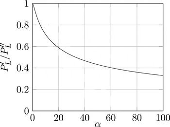
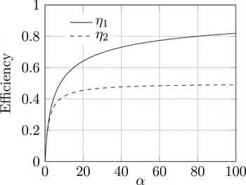
Figure 9 shows the behavior of the ratio between the output power provided by the maximum efficiency solution (
 ${P^{\prime}_L}$
) and by the maximum power solution (), which also represents the available output power of the WPT system. The corresponding efficiencies are reported in Fig. 10. It can be observed that, as the figure-of-merit α is increased,
 ${P^{\prime}_L}$
becomes a smaller fraction of the available power.
Ratio between output power in maximum efficiency conditions (
 ${P^{\prime}_L}$
) and maximum output power (
 ${P^{\prime\prime}_L}$
) as a function of the figure-of-merit α.

Efficiency: continuous line corresponds to the maximum efficiency solution; dashed line corresponds to the solution, which maximizes the power on the load.

B) Coupled inductances with a capacitive T network on the primary side
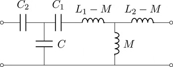
In this section, we investigate the network presented in [Reference Costanzo, Dionigi, Mastri, Mongiardo, Russer and Russer28] and reproduced in Fig. 11. Following the derivation provided in [Reference Costanzo, Dionigi, Mastri, Mongiardo, Russer and Russer28] we can select the component values in order to realize a 1:n transformer by choosing:
 $$C = \displaystyle{n \over N}\displaystyle{1 \over {\omega _0^2 {k_0}{L_1}}}, $$
 $${C_1} = C\displaystyle{{{k_0}} \over {(n/N) - {k_0}}}, $$
 $${C_2} = C\displaystyle{{{k_0}} \over {(N/n) - {k_0}}}. $$
Coupled inductors with a capacitive T added on the primary side.

By constructing the chain matrix (ABCD) for the circuit of Fig. 11 we obtain the general ABCD matrix and from the latter we can compute the impedance matrix; its elements take the following form:
 $${z_{11}} = \displaystyle{{({X_0}{Q_1}{u^2} - j{X_0}u + (k_0^2 - 1){X_0}{Q_1}){N^2}} \over {j{Q_1}{n^2}{u^3} + {n^2}{u^2} - j{Q_1}{n^2}u}},$$
 $${z_{12}} = \displaystyle{{{k_0}{X_0}{Q_1}ku{N^2}} \over {j{Q_1}n{u^2} + nu - j{Q_1}n}},$$
 $$\eqalign{z_{22} = & \displaystyle{\matrix{\left[{X_0}{Q_1}{Q_2}({k^2} - 1){u^3} + j{X_0}({Q_1} + {Q_2}){u^2} \right. \cr \left.+ {X_0}({Q_1}{Q_2} + 1)u - j{X_0}{Q_1} \right]{N^2}} \over {j{Q_1}{Q_2}{u^2} + {Q_2}u - j{Q_1}{Q_2}}}.}$$
When the impedance matrix is computed at the nominal frequency u = 1 and for the nominal coupling k = k 0, we obtain:
 $$\left[ {\matrix{ {\displaystyle{{(k_0^2 {X_0}{Q_1} - j{X_0}){N^2}} \over {{n^2}}}} & {\displaystyle{{k_0^2 {X_0}{Q_1}{N^2}} \over n}} \cr {\displaystyle{{k_0^2 {X_0}{Q_1}{N^2}} \over n}} & {\displaystyle{{{X_0}(k_0^2 {Q_1}{Q_2} + j{Q_2} + 1){N^2}} \over {{Q_2}}}} \cr}} \right]. $$
It is important to note that, contrary to the previous case of mutually coupled inductors, in this case, at the nominal values, we have x
12 = 0 and r
12 ≠ 0. From the latter, by introducing the parameter α defined as
 $\alpha = k_0^2 {Q_1}{Q_2}$
we recover for this case:
 $${\chi ^2} = 0, $$
 $${\xi ^2} = \displaystyle{{k_0^2 {Q_1}{Q_2}} \over {k_0^2 {Q_1}{Q_2} + 1}} = \displaystyle{\alpha \over {1 + \alpha}}, $$
 $${\theta _r} = \displaystyle{1 \over {\sqrt {1 + \alpha}}}, $$
 $${\theta _x} = 0. $$
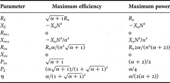
The expressions for the various parameters of interest can be readily computed and are summarized in Table 3. In particular, it can be observed that the expressions of the efficiency are identical to those obtained in the previous case and that, even if the expressions of the output power are different, also the ratio between
 ${P'_L}$
and
 ${P''_L}$
is the same. Hence the results shown in Figs 9 and 10 hold in this case, too.
A summary of the parameters’ values for the approaches that maximize efficiency and power in the case of a capacitive T on the primary side.

The parameters have the following meanings:
 $\alpha = k_0^2 {Q_1}{Q_2}$
and R
0 = X
0
N
2/Q
2. Note that the quantities P
in
, PL
, are normalized with respect to
 ${P_0} = V_1^2 /(2{r_{11}})$
. In the present case, we have r
11 = R
0
α/n
2.
Table 3 also shows that the reactive part of the load impedance X L corresponds to a capacitance of value
 $${C_L} = \displaystyle{1 \over {\omega _0^2 {L_2}}}, $$
as in the previous case, while the matching reactance X m1 corresponds to an inductance of value L 1 N 2/n 2. Making use of (42) we obtain that the series connection of X m1 and C 2 is equivalent to a single inductance
 $${L_{eq}} = {k_0}{L_1}\displaystyle{N \over n}, $$
hence it is possible to reduce the value of the matching inductance and to simplify the circuit by eliminating the capacitor C 2.
1) THE CONSTANT POWER SOLUTION FOR (ALMOST) ANY COUPLING
Let us denote with
 ${\bar P_L} = {P_L} \cdot {P_0}$
the output power (not normalized). It is apparent that, for the maximum power on the load solution, the optimum load is always R
0 and does not depend on coupling. Hence we have:
 $${\bar P_L} = {P_L} \cdot {P_0} = \displaystyle{{V_1^2} \over 2}\displaystyle{{{n^2}} \over {4{R_0}}} = \displaystyle{{V_1^2} \over 2}\displaystyle{{{n^2}} \over {{N^2}}}\displaystyle{{{Q_2}} \over {4{X_0}}}. $$
Since equation (50) does not depend on the coupling k 0, we have the same amount of power on the load for different values of coupling. Naturally, in the present analysis the capacitive Tee has been considered lossless. When the coupling decreases the value of the capacitances increase and their losses becomes relevant. However, as long as the losses on the capacitive Tee are negligible we can theoretically achieve the same maximum power for different values of the coupling.
As a final note we would also like to remark that, in the coupled inductors case, the load resistance that realizes maximum power transfer is greater than the load resistance that realize maximum efficiency. For this case the load resistance value R
L
should be such that
 $(1 + \alpha ){R_0} \gt {R_L} \gt \sqrt {1 + \alpha}\; {R_0}$
. On the other hand, for the configuration that realizes the 1:n transformer, the load resistance for the maximum efficiency case is always greater than the one that realizes maximum power transfer. In this case, the load resistance should be
 $\sqrt {1 + \alpha}\; {R_0} \gt {R_L} \gt {R_0}$
. It is apparent that, depending on the desired value of the load resistance, one of the two configurations may be preferred.
IV. A CASE STUDY
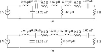
As a case study, let us consider the circuit represented in Fig. 12(a). The circuit has been designed, according to the theory developed in the previous section, in order to realize a transformer with n = 0.28 when operating at the frequency of 1 MHz and with a coupling factor k 0 = 0.1. Two commercial inductors (Würth Elektronik WE-WPCC model no.760308111) have been chosen for the inductive link. The nominal value of their inductance is 6.3 µH and their nominal Q factor at 1 MHz is 80, resulting in a resistance of 0.5 Ω, as shown in Fig. 12(a). Since the two inductances are equal, in this case we have N = 1. The inductance and the two capacitances of the input matching network have been computed by (49), (40), and (41), respectively, and the output capacitance has been computed by (48). The value of the load resistance, given by Table 3, is R L = 4 Ω if the system is designed for maximum efficiency and R L = 0.5 Ω if the system is designed for maximum output power.
Coupled inductors with a capacitive T added on the primary side. (a) Nominal circuit and (b) manufactured circuit. A matching inductance has been introduced between the generator and the two-port network. A 4 Ω load resistance has been computed for maximum efficiency, giving an input impedance R in = 50 Ω. In maximum output power condition, the load would be R L = 0.5 Ω and the input resistance R in = 12 Ω. Note that the inductances L 1, L 2 have the nominal value of 6.3 µH (6.12 µH in the manufactured circuit); the series inductances of value 5.67 µH in the nominal circuit (5.508 µH in the manufactured circuit) in the present figure are L 1 − M and L 2 − M, respectively.

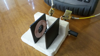
The circuit has then been assembled and measured as shown in Fig. 13. The component values have been singularly measured and are reported in Fig. 12(b). In the following, we will address the circuit of Fig. 12(a) as the nominal circuit and the circuit of Fig. 12(b) as the manufactured circuit. The measured inductance of the link inductors is 6.12 µH and their measured Q factor is 77.9. A four turn spiral coil on an 11 mm diameter ferrite rod with measured Q factor 131 has been used to realize the input matching inductor. The matching networks have been realized by means of high Q ceramic capacitors.
The manufactured circuit.

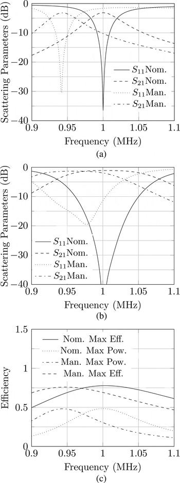
The simulated scattering parameters of the nominal and manufactured circuits are reported in Fig. 14. The maximum output power condition is shown in Fig. 14(a) and the maximum efficiency condition is shown in Fig. 14(b). These results show a perfect matching for the nominal circuit at 1 MHz. On the other hand, the manufactured circuit exhibits a degradation of the response and a shift of the matching point to lower frequency, due to the discrepancies between the nominal and the actual component values. In Fig. 14(c), the power transmission efficiencies are shown, confirming a frequency shift for the manufactured circuit both in the maximum output power and in the maximum efficiency condition.
Simulation results: (a) comparison of simulated scattering parameters in maximum output power condition for the nominal and the manufactured circuit (input port impedance R in = 12 Ω, output port impedance R L = 0.5 Ω); (b) comparison of simulated scattering parameters in maximum efficiency condition for the nominal and the manufactured circuit (input port impedance R in = 50 Ω, output port impedance R L = 4 Ω); (c) comparison of power transmission efficiency in maximum efficiency and maximum output power condition for the nominal and the manufactured circuit.

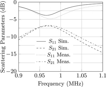
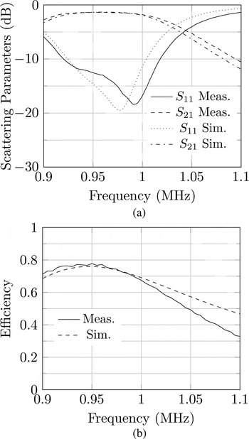
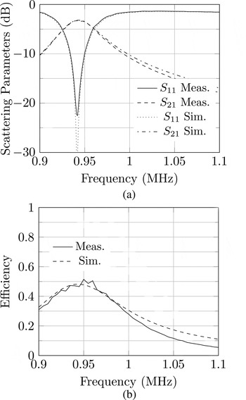
The measured scattering parameters and their simulated values for the manufactured circuit are reported in Fig. 15. These results have been obtained making use of a common value of 50 Ω for both the input and the output port reference resistance. Hence, in order to determine the circuit response in maximum efficiency condition we have renormalized the measured scattering parameters assuming a reference impedance of 50 Ω for the input port and of 4 Ω for the output port, while in maximum output power condition we assumed a reference impedance of 12 Ω for the input port and of 0.5 Ω for the output port.
Simulation and measurement results: manufactured circuit simulation and measured scattering parameters with ports impedance 50 Ω.

The results obtained in maximum efficiency condition are shown in Figs 16(a) and 16(b) demonstrating a very good agreement of the measured power transmission efficiency with the simulated one for the manufactured circuit. Due to the frequency shift caused by component tolerances and to the additional contributions to losses arising from the matching networks, the measured efficiency obtained at the frequency of 1 MHz is about 68% instead of 78%, predicted using the equation of Table 3 in ideal conditions. However, an efficiency of 73% is achieved at the maximum of the efficiency curve of the manufactured and measured circuit.
Simulation and measurement results: (a) manufactured circuit simulation and measured scattering parameters in maximum efficiency condition with input port impedance R in = 50 Ω and output port impedance R L = 4 Ω; (b) power transmission efficiency in maximum efficiency condition.

The same procedure has been applied in the case of maximum output power, the results are shown in Fig. 17. The very good agreement between the manufactured circuit simulation and the measured one is apparent.
Simulation and measurement results: (a) manufactured circuit simulation and measured scattering parameters in maximum output power condition with input port impedance R in = 12 Ω and output port impedance R L = 0.5 Ω; (b) power transmission efficiency in maximum output power condition.

V. CONCLUSION
The problem of magnetic resonant WPT has been considered from a rigorous viewpoint. It has been shown that the wireless channel between a transmitter and a receiver can be represented by a two-port network. Given the network parameters, the solution which maximizes the efficiency and the solution which maximizes the power on the load have been derived.
Two possible realizations of the wireless channel have been considered: mutually coupled inductors and mutually coupled inductors with an additional inverter that realizes a 1:n transformer. The maximum efficiency solution and the maximum output power solution have been obtained for both cases. In this way, the correct matching networks and load impedance have been established. Noticeably, when considering the network configuration that realizes the 1:n transformer, the load resistance required in the maximum power solution does not depend on coupling.
The proposed approach allows us to design the wireless channel in a systematic way and avoids problems related to frequency shift and bifurcation of solutions.
 Alessandra Costanzo is an Associate Professor of Electromagnetic Fields at the University of Bologna, Italy. She has authored more than 140 scientific publications on peer reviewed international journals and conferences, three chapter books, and she holds three international patents. She has developed innovative software platform for the nonlinear/electromagnetic co-simulation of RF systems, excited by modulated sources demonstrating circuit-level analysis of entire MIMO and UWB links, including realistic channel models. She is now involved in wearable energy-autonomous sensors and wireless power transfer systems. She is MC member of the EU COST action WiPE “Wireless power transfer for sustainable electronics” and she chairs WG1: “far-field wireless power transfer”. She is member of the TPC board member of MTT-S IMS, EUMW, WPTC, and RFID-TA ICUWB. She is the vice chair of IEEE MTT-S TC-26 “Wireless Energy Transfer and Conversion” and member of IEEE MTT-S TC-24 RFID Technologies. She is IEEE senior member.
 Marco Dionigi has received the Laurea degree (110/110 cum laude) in Electronic Engineering from the University of Perugia. He achieved at the same university the title of Ph.D. In 1997, he became an Assistant Professor at the Faculty of Engineering of the University of Perugia. He took part in several research project regarding the development of software tools for waveguide and antenna fullwave simulation, the development of permittivity and moisture microwave sensors, the development of a SAR and ultrawideband antennas. He was the coauthor of a paper that was awarded the “Young Engineers Prize” at the European Microwave Conference 2005 in Paris. He is now involved in the study and development of high efficient wireless electromagnetic power transfer for industrial applications. He is author of more than 70 papers on international journal and conferences.
 Franco Mastri received the Laurea degree (100/100 cum laude) in Electronic Engineering from the University of Bologna, Italy, in 1985. From 1990 to 2004, he was a Research Associate with the Department of Electrical Engineering, University of Bologna, where he has been an Associate Professor of Electrotechnics since 2005. His main research interests include nonlinear-circuit simulation and design techniques (with special emphasis on CAD techniques for large-size problems), nonlinear RF device modeling, nonlinear/RF co-simulation of RF systems, and stability and noise analysis of nonlinear circuits.
 Mauro Mongiardo has received the Laurea degree (110/110 cum laude) in Electronic Engineering from the University of Rome “La Sapienza” in 1983. In 1991 he became an Associate Professor of Electromagnetic Fields and since 2001 he has been a full Professor of Electromagnetic Fields at the University of Perugia. He has been elected Fellow of the IEEE for “For contributions to the modal analysis of complex electromagnetic structures” in 2011.
The scientific interests of Mauro Mongiardo have concerned primarily the numerical modeling of electromagnetic wave propagation both in closed and open structures. His research interests have involved CAD and optimization of microwave components and antennas.
Mauro Mongiardo has served in the Technical Program Committee of the IEEE International Microwave Symposium from 1992; since 1994 he has been the member of the Editorial Board of the IEEE Transactions on Microwave Theory and Techniques. During the years 2008–2010 he has been an Associate Editor of the IEEE Transactions on Microwave Theory and Techniques. He is author or co-author of over 200 papers and articles in the fields of microwave components, microwave CAD, and antennas. He is the co-author of the books “Open Electromagnetic Waveguides” (IEE, 1997), and “Electromagnetic Field Computation by Network Methods” (Springer, 2009). Recently, he has co-authored a chapter in the book Wireless Power Transfer – Principles and Engineering Explorations (Intech, 2012), and a chapter in the book Wireless Power Transfer (River publishers, 2012).
 Johannes A. Russer received his Diplom Ingenieur degree in Electrical Engineering and Information Technology from the Universität Karlsruhe, Germany, in 2003. In 2004, he joined the University of Illinois at Urbana-Champaign as a Research Assistant in pursuit of his Ph.D. degree. He has graduated in May 2010 with a Ph.D. thesis on “Methodologies for electromagnetic field modeling for computer aided analysis of multi-domain physical interactions”.
Since May 2010 Johannes Russer has been working as a Postdoctoral Research Fellow at the Institute for Nanoelectronics of the Technische Universität München. He is working there on the near-field characterization of electromagnetic interference and on methods for numerical modeling of stochastic electromagnetic fields. His research interests concern numerical electromagnetics, network methods in electromagnetic field modeling, multiphysics modeling, and multiscale modeling.
Johannes Russer is a member of the IEEE, of the German Informationstechnische Gesellschaft (ITG) and of the Eta Kappa Nu honor society.
 Peter Russer received his Dipl.-Ing. (M.S.E.E.) degree in 1967 and the Dr., techn. (Ph.D.E.E.) degrees in 1967 and 1971, respectively, both from the Vienna University of Technology, Austria. In 1971 he joined the Research Institute of AEG-Telefunken in Ulm, Germany, where he worked on fiber optic communication, broadband solid-state electronic circuits, statistical noise analysis of microwave circuits, laser modulation, and fiber optic gyroscopes. With his research group he realized in 1978 the first optical fiber transmission link for 1 Gbit/s worldwide. From 1981 to 2008 Peter Russer has been the Professor and Head of the Institute for High Frequency Engineering at the Technische Universität München (TUM), Germany. From October 1992 to March 1995, he also has been Director of the Ferdinand-Braun-Institut für Höchstfrequenztechnik, Berlin. Since 2008 he has been Emeritus of Excellence of the TUM and he is now with the Institute for Nanoelectronics of the TUM In 2007 Peter Russer co-founded the Spin-Off company Gauss Instruments GmbH which is now a leading manufacturer of systems for time-domain measurement of electromagnetic interference.
Peter Russer has published five books and more than 900 scientific papers in refereed journals and conference proceedings. He is Life Fellow of the IEEE, member of acatech, the German Academy of Science and Engineering. In 2006 he received the Distinguished Educator Award, and in 2012 the Pioneer Award, both of the IEEE MTT Society and in 2009 he received the Distinguished Service Award from the European Microwave Association (EuMA). In 2007 Peter Russer received an honorary Doctor degree from the Moscow University of Aerospace Technologies (MAI). In 2010 Peter Russer has been awarded the Golden Ring of Distinction of the VDE.