Introduction
Microwave bandpass filters with reconfigurable band traps are critical components in modern microwave systems, extensively employed in applications such as radar, signal processing, wireless communications, national defense and so on. Their primary function is to effectively suppress unwanted signals within specific frequency bands in dense microwave environments. An ideal bandstop filter is characterized by low out-of-band loss, high stopband rejection, reconfigurable bandwidth, and frequency agility [Reference Zhang, Chan, Xue and Hu1]. The study of bandpass filters with reconfigurable band traps filters has yielded a series of achievements recently. Qin et al. presented a methodology for integrating reconfigurable filters into antenna feeding lines, employing PIN diodes to control the operating states of antennas [Reference Qin, Wei and Guo2]. Girish has introduced a bandstop filter based on stimulated Brillouin scattering (SBS), which addresses the power efficiency limitations inherent in traditional SBS-based approaches, thereby achieving reduced out-of-band loss [Reference Girish, Parihar, Raj and Choudhary3]. By employing only two stimulated Brillouin scattering (SBS) responses—a gain resonance and a loss resonance—and integrating them with advanced phase engineering techniques, a low-power, low-loss broadband bandstop filter was achieved. A CMOS-based bandstop filter is proposed in [Reference Kim, Lee, Lee, Jung and Chappell4], capable of delivering in-band attenuation in the range of 30-60 dB. This design optimizes the balance between the coupling strength, overall parameter settings, and the Q-factor of the system components. However, due to the complexity of both the design principles and the implementation process, this filter is hardly used in practical applications. As a result, there is a need for bandstop filters with simpler design principles and structures. One such filter, utilizing defected ground structures (DGS), was introduced in [Reference Liang, Sun, He and Wang5]. This design enhances the trapping performance by incorporating three DGS structures, yielding three transmission zeros. While this approach offers scalability, it is constrained by fixed transmission zero positions once the dimensions are set, limiting its flexibility in certain applications. Current research demonstrates that numerous filter circuits integrating lumped and distributed elements have been developed, exhibiting enhanced flexibility and improved compatibility [Reference Ebrahimi, Baum, Scott and Ghorbani6, Reference Li7]. When implemented in RF communication systems, these hybrid configurations can significantly reduce the physical footprint of the system while maintaining optimal performance. However, the inclusion of numerous lumped components adds complexity to the design and restricts its tunable range. A balanced reconfigurable dual-band bandpass filter with constant absolute bandwidth was proposed in [Reference Wei, Zhang, Zeng and Shi8], which reduces diode usage through asymmetrically stub-loaded structures while maintaining the advantage of low insertion loss. A compact, reconfigurable THz filter utilizing the technology of spoof surface plasmonics is capable of performing spectral imaging, which can be used in polymer industries [Reference Ram, Kartikeyan and Yuvaraj9]. Due to the fabrication limitations at the THz regime, the proposed filter design is verified at microwave frequencies. A novel ultra-wideband balanced bandpass filter featuring harmonic suppression and high selectivity was proposed in [Reference Zhao, Wang, Liu and Fang10], which employs quarter-wavelength asymmetric parallel-coupled transmission lines to achieve sharp filtering selectivity.
As technology advances, the development of bandstop filters with reflection-free characteristics at the input has gained increasing attention. Through the incorporation of loss resonators, reflectionless bandstop filters can theoretically achieve near-infinite attenuation. Zuo and Feng proposed a planar bandstop filter design that offers flexible design parameters, highly selective dual-frequency bandstop functionality, and excellent wave-absorbing characteristics [Reference Zuo, Qin, He, Mei and Li11, Reference Feng, Hong, Che and Xue12]. Additionally, a bridged T-network absorptive filter was introduced in [Reference Chieh and Rowland13], which enhances design flexibility, minimizes the number of required elements, and achieves significant attenuation while maintaining a compact form factor. However, the design of absorptive filters remains relatively complex, primarily due to the integration of multiple lumped elements. Therefore, there is a pressing need for bandstop filters that feature a simplified design process, reduced structural complexity, reconfigurable capabilities, and a broad tuning range. Such designs would not only streamline the manufacturing process and lower costs, but also enhance filter performance and application versatility. A novel compact and low-loss microstrip ultra-wideband (UWB) bandpass filter featuring a narrow notch band is proposed. The notch band is achieved through the integration of two stepped-impedance stubs, offering effective suppression of unwanted signals within the designated frequency range [Reference Sen and Moyra14]. Besides, a compact planar UWB bandpass filter exhibiting four distinct notched bands and low insertion loss is presented in [Reference Gao, Xu, Nan and Wang15]. The realization of the quad notched bands is facilitated through precise tuning of the dimensions of a multiple-mode resonator (MMR) and a defected ground structure (DGS). Nevertheless, the notch structures proposed in the above-mentioned studies feature fixed center frequencies, thereby lacking the desired flexibility. Addressing this limitation constitutes a key objective of the present work.
In this article, we propose a new bandpass filter with reconfigurable band traps, complemented by a control system utilizing a microcontroller unit (MCU) to enable precise tuning of the stopband frequency. The reconfigurability of the stopband is achieved by loading quarter-wavelength resonators to introduce transmission zeros in the passband, with varactor diodes integrated at the ends of the resonators to adjust the capacitance. This design offers several advantages, including a wide tuning range, low insertion loss, a straightforward design methodology, high scalability, excellent programmability via an MCU-based voltage control system, and robust bandwidth performance.
Circuit analysis and design
The filter proposed in this manuscript achieves its stopband function by integrating a reconfigurable trap structure within the bandpass filter. It provides the theoretical analysis and design considerations for both the bandpass filter and the incorporated trap structure in this section.
Theoretical analysis of planar S-band bandpass filter
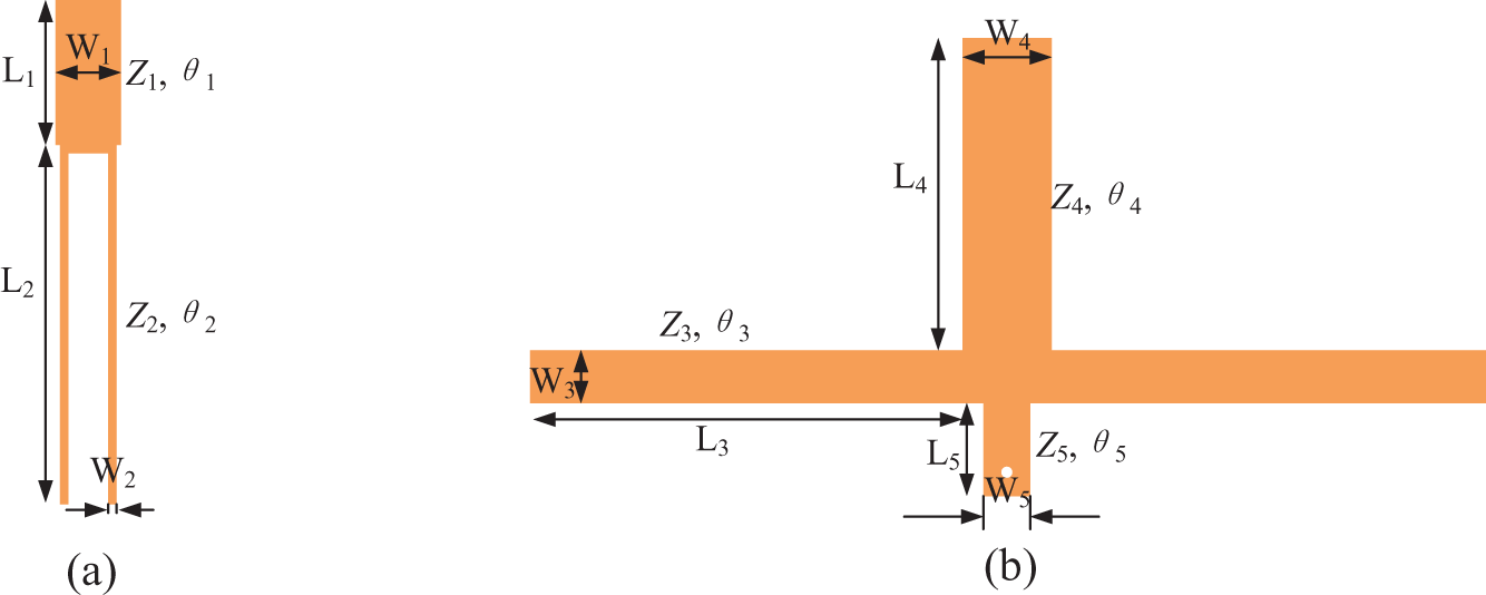
A wideband bandpass filter designed based on the principles of a third-order Butterworth bandpass filter with step impedance resonator is proposed, which owns superior performance in highly symmetrical structure and integration with external circuits [Reference Nouri, Nkenyereye, Hafez, Hazzazi, Chaudhary and Assaad16]. The fundamental structure of the resonator used in this wideband bandpass filter is depicted in Figures 1(a) and (b), where Z 1 to Z 5 denote the characteristic impedances and θ 1 to θ 5 denote the electrical lengths of the respective sections within the resonator. The specific parameters of the resonator are listed in Table 1. A theoretical analysis of the resonator structure is presented in the following.
(a) The prototype of resonator 1 and (b) resonator 2.

The values of the physical parameters and corresponding electricals parameters

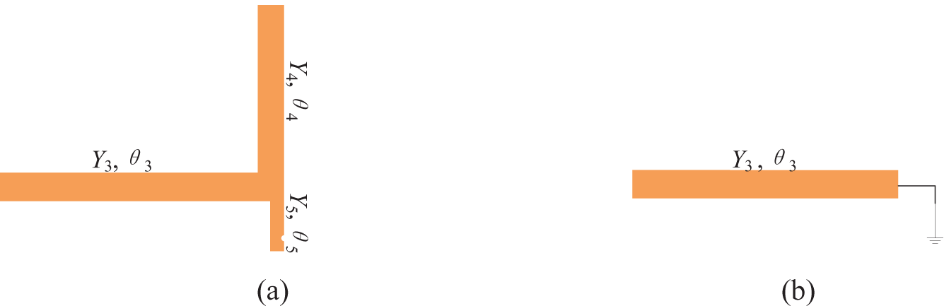
The odd and even mode analysis of the resonator 2 structure is performed as shown in Figure 2, where Y 3, Y 4 and Y 5 represent the equivalent admittance, and θ 3, θ 4 and θ 5 denote the electrical lengths of the microstrip lines in the odd-even mode model of the resonator, respectively.
According to the conduction equation of lossless transmission line as in equation (1) [Reference Lu, Liu, Liao, Wang, Huang and Xi17]:
 \begin{equation}
{{Y}_{in}}={{Y}_{0}}\frac{{{Y}_{L}}+j{{Y}_{0}}\tan \beta l}{{{Y}_{0}}+j{{Y}_{L}}\tan \beta l}.
\end{equation}
The odd and even-mode resonant frequencies of this resonator can be derived as the equation associated with admittance, where Yin, YL, Y 0, β and l represent the input admittance, load admittance, characteristic admittance, phase constant, and the distance from the termination, respectively.
(a) Resonator 2 even mode and (b) 2 odd mode.

The resonator can be decomposed into three resonant units with different impedances and electrical lengths to analyze the even-mode resonant frequency, which can be modeled as a cascade of three transmission lines. This transmission line cascade is represented by the ABCD matrix, where the individual transmission line impedances are accounted for, leading to equation (2) through matrix multiplication:
 \begin{equation}
Y_{in,even}=-jY_{3}\frac{Y_{5}-Y_{4} \tan \theta _{4}\tan \theta _{5}-Y_{3}\tan \theta _{3}\tan \theta _{5} }{Y_{3}\tan \theta _{5}+ Y_{5}\tan \theta _{3}-Y_{4}\tan \theta _{3}\tan \theta _{4}\tan \theta _{5} }.
\end{equation}
The resonant frequency during even mode excitation is obtained by making its input conductance  $Y_{in,even}=0$.
Similarly, when deriving the odd mode resonant frequency, the resonator can be viewed as two resonant units with different impedances and electrical lengths. Equation 3 can be obtained:
 \begin{equation}
Y_{in,odd}=\frac{-jY_3}{\tan \theta _3}.
\end{equation}
The resonance condition under odd mode excitation is: 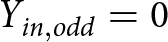 $Y_{in,odd}=0$.
It is evident that the conductance and electrical length of each section of the transmission line influence the resonant frequency of the resonator. Based on this theory, the dimension of this resonator can be derived easily.
Besides, the microstrip resonators discussed in this article are designed using stepped impedance stubs. Their approximate dimensions can be readily calculated using equations (4)–(8) provided below. This calculation is based on the capacitance and inductance values of the LC resonators, extending the design methodology to microstrip structures via lumped element models [Reference Majidifar18].
When w/h<1
where
 \begin{equation}
\begin{aligned}
& {{Z}_{c}}=\frac{\eta }{2\pi \sqrt{{{\varepsilon }_{re}}}}\ln [8\frac{h}{w}+0.25\frac{w}{h}] \\
& {{\varepsilon }_{re}}=\frac{{{\varepsilon }_{r}}+1}{2}+\frac{{{\varepsilon }_{r}}-1}{2}\{{{[1+12\frac{h}{w}]}^{-0.5}}+0.04{{[1-\frac{w}{h}]}^{2}}\} \\
\end{aligned}
\end{equation}
When w/h≥1
where
 \begin{equation}
\begin{aligned}
& {{Z}_{c}}=\frac{\eta }{\sqrt{{{\varepsilon }_{re}}}}{{\{\frac{h}{w}+1.393+0.677\ln [\frac{w}{h}+1.444]\}}^{-1}} \\
& {{\varepsilon }_{re}}=\frac{{{\varepsilon }_{r}}+1}{2}+\frac{{{\varepsilon }_{r}}-1}{2}{{[1+12\frac{h}{w}]}^{-0.5}} \\
\end{aligned}
\end{equation}
 \begin{equation}
{{v}_{p}}=\frac{c}{\sqrt{{{\varepsilon }_{re}}}}
\end{equation}
 \begin{equation}
L=\frac{l{{Z}_{c}}}{{{v}_{p}}}
\end{equation}
 \begin{align}
C& =[8.85 \ast {{(10)}^{-12}}{{\{{{(\frac{{{\varepsilon }_{r}}w}{h})}^{1.08}}+{{[\frac{2\pi ({{\varepsilon }_{r}}+1)}{2}}}}} \nonumber \\ & \qquad {{{{\ast(\frac{1}{\ln (\frac{8h}{w}+1)}-\frac{w}{8h})]}^{1.08}}\}}^{0.926}}]l
\end{align}
where Zc,  $\varepsilon_{re}$, η, c, vp, L, C, w, l, h and
 $\varepsilon_{r}$ represent the characteristic impedance, effective dielectric constant, intrinsic impedance of free space (120
 $\pi\Omega$), speed of light, phase velocity, inductance, capacitance, microstrip line width, microstrip line length, dielectric substrate thickness, and relative permittivity of the substrate, respectively.
The dimensions of the microstrip resonator are determined by the required inductance and capacitance values. The substrate characteristics are defined by h, after which an appropriate value for w is selected based on the chosen substrate. The values of Zc and  $\varepsilon_{re}$ are then computed using equation (4) or equation (5), depending on the parameters h and w, respectively. Subsequently, equation (6) is applied to determine the phase velocity. The length of the microstrip line corresponding to the inductance value is calculated using equation (7), while the length associated with the capacitance value is obtained from equation (8).
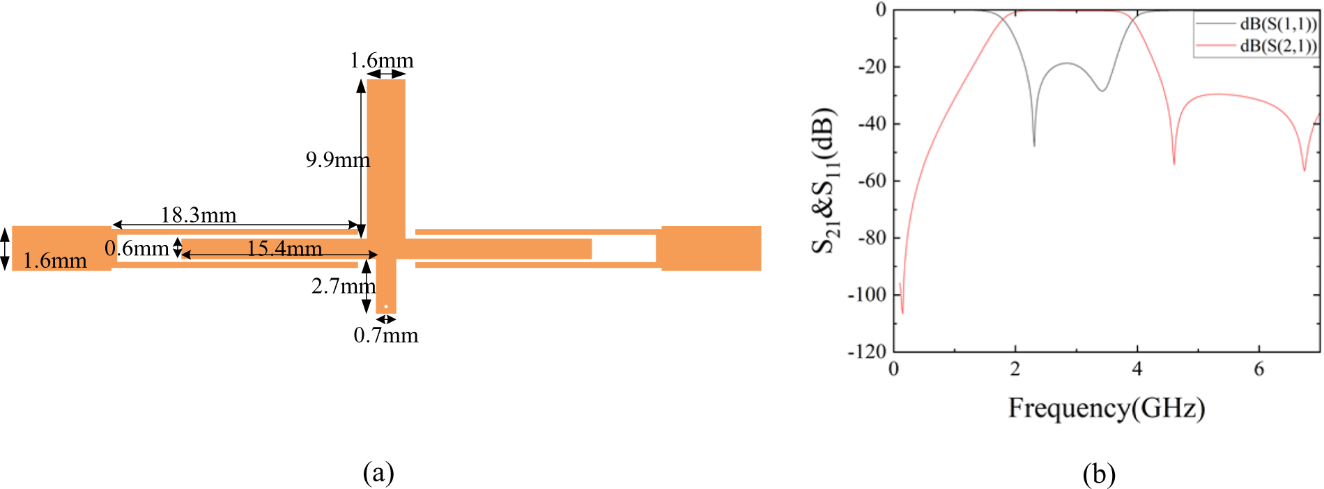
(a) The prototype of bandpass filter and (b) S-parameter of bandpass filter.

Based on the parity-mode resonant frequency analysis and the microstrip line dimension determination described above, the topology and dimensions of the broadband bandpass filter used in this article are shown in Figure 3(a). The corresponding simulation results are presented in Figure 3(b). The filter achieves a bandwidth of 2 GHz, with an in-band insertion loss of 0.3 dB, a return loss better than −17 dB, and an out-of-band rejection exceeding −50 dB, demonstrating relatively good performance.
Design of open-ring planar trap structures
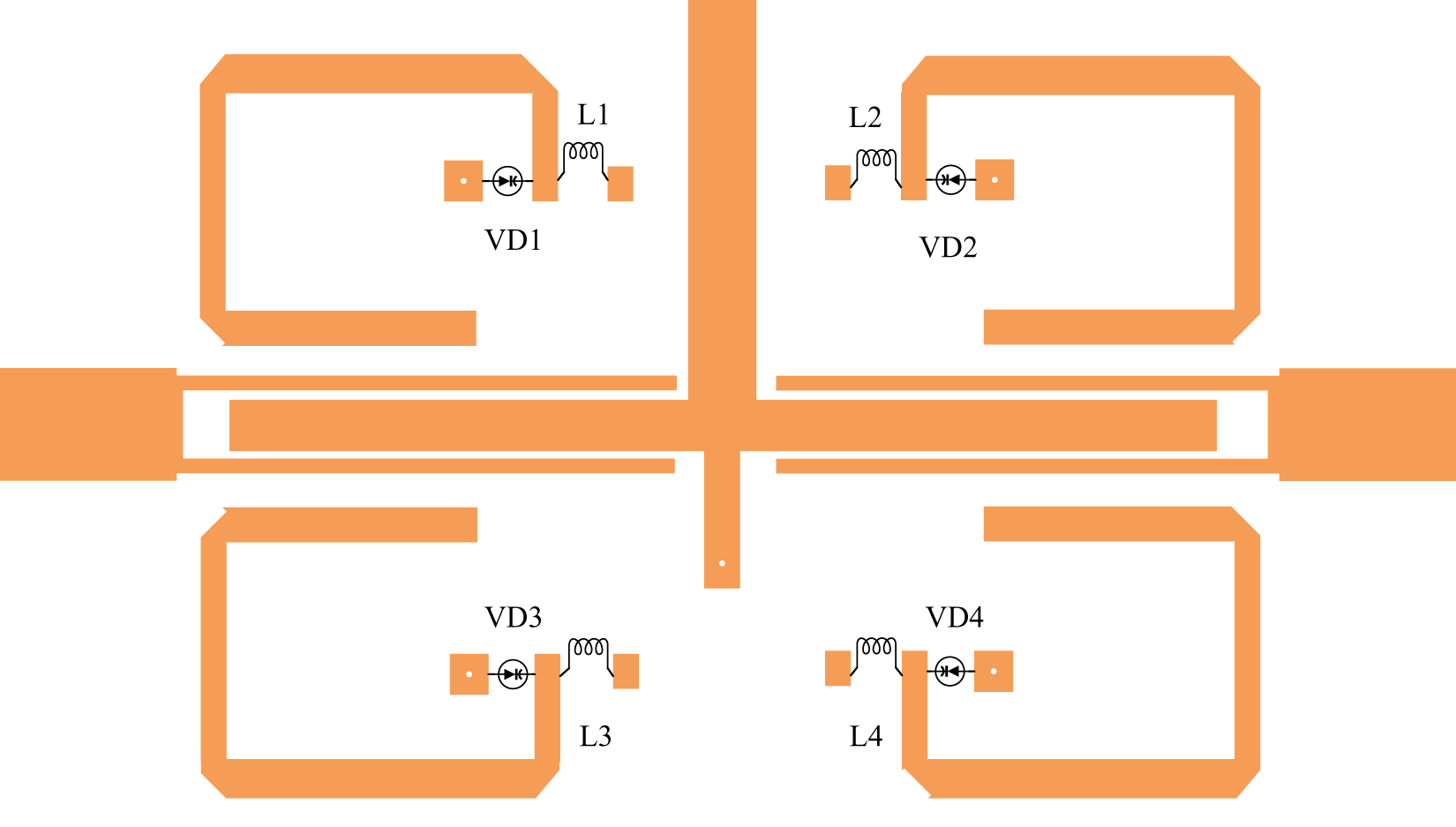
Although the broadband bandpass filter described in the previous section effectively eliminates frequencies outside the designated band, it is unable to mitigate clutter within the passband. To address this limitation and filter signals within specific frequency ranges, we propose an open-ring trap structure in this section. This structure is capable of suppressing unwanted signals within narrow bands. The planar trap structure is shown in Figure 4(a), consisted of four quarter-wavelength resonators. By bending the structure, the occupied area is reduced without degrading the trapping performance.
(a) Open-ring structural version and (b) Open-ring intrinsic imitation truth result.

The harmonic characteristics of the structure are analyzed by simulating its eigenmodes, and the length of the resonator is changed from 23 mm to 27 mm in 1mm increments, with the simulation results shown in Figure 4(b). We finally chose the 25 mm, because the characteristics after combining a varactor diode are fitting the demand of design. The results indicate that the structure exhibits four resonant points around 3.5 GHz, and its higher harmonics do not negatively impact the passband performance of the filter.
The trap structure can be tuned to set its initial frequency position by adjusting the line length. The in-band trapping capability of the bandpass filter is realized by integrating the trap structure into the previously discussed bandpass filter. Mathematical calculations and layout optimizations are conducted using electromagnetic simulation software to fine-tune the circuit’s physical dimensions and achieve the desired performance objectives.
A wideband bandpass filter with reconfigurable band traps design
While the bandpass filter with the added trap structure in Section “Design of open-ring planar trap structures” allows for tuning of the trap’s position by altering the line length, this adjustment requires modifications to the circuit topology. To overcome this limitation, a varactor diode can be integrated at one end of the resonator, enabling frequency reconfiguration of the trap via the variable capacitance of the diode’s junction. As shown in Figure 5, the proposed bandpass filter with reconfigurable band traps consists of a main transmission path and four symmetrically coupled trap structures. These four reconfigurable traps control a single transmission zero point simultaneously. Since the filter system accommodates both radio frequency (RF) and direct current (DC) signals, a DC-alternating current (AC) blocking structure is required during testing. The coupled trap structure ensures that DC signals do not interfere with the main signal path. RF signals are directed into the DC-regulated power supply through the coupling line, which may affect the power supply. To mitigate RF signal loss and prevent interference with the power supply, an inductor is placed at the power input. The varactor diode is grounded, and the high-frequency inductance on the opposite side is adjusted to modify the capacitance, thereby tuning the resonant frequency of the trap structure.
The prototype of reconfigurable filter.

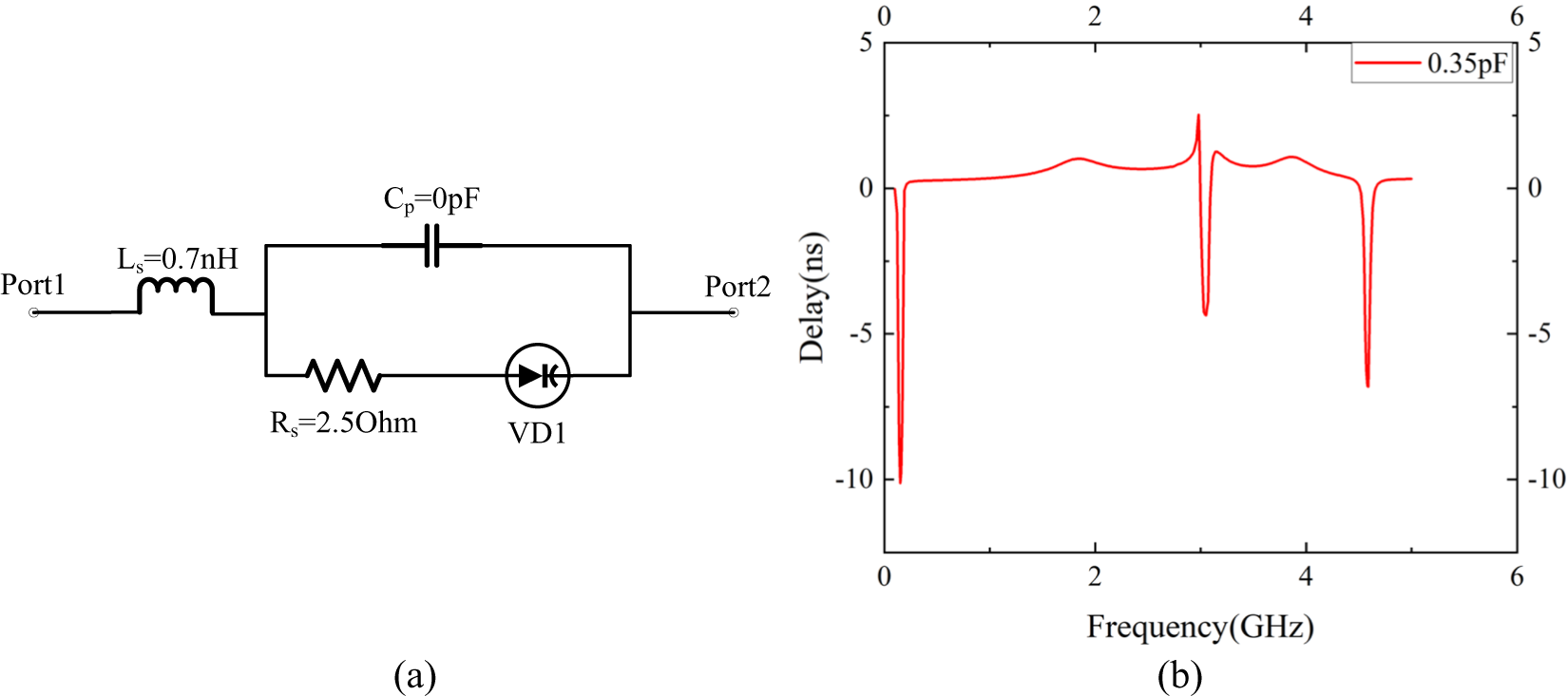
The varactor diode model is the SMV-2020. The equivalent circuit of the varactor diode along with its parasitic parameters is shown in Figure 6(a). The capacitance of the varactor diode is not frequency-dependent, but it is related to the applied reverse bias voltage. However, in practical operation, the junction capacitance of a varactor diode depends not only on the applied reverse bias voltage but also exhibits slight attenuation with increasing operating frequency. This frequency dependence primarily arises from material losses, limitations in carrier response time, and the presence of parasitic elements. As the frequency increases, the effective capacitance tends to decrease slightly, while the equivalent series resistance (R s) increases, thereby affecting the quality factor (Q-factor) of the diode. In the present design, the operating frequency range is from 2.1 GHz to 3.0 GHz. Within this range, the impact of its frequency dependence on the overall circuit performance is considered minor. Nevertheless, to ensure accuracy, the parasitic elements have been taken into account in the equivalent model during simulation, and the consistency of the frequency response has been verified experimentally. The reverse voltage corresponding to capacitance values is shown in Table 2.
(a) The equivalent circuit of SMV-2020 and (b) the group delay of the filter when the capacitance is 0.35 pF.

C-V values of varactor diode

The group delay simulation of this filter is also shown in Figure 6(b) when the capacitance is 0.35 pF. Significant variations and sharp peaks (or notches) are observed in the group delay of the filter around 3 and 4.2 GHz, where the group delay rapidly shifts to negative values, approaching nearly -10 ns. This phenomenon typically indicates the presence of transmission zeros or filter edge frequencies in those regions. In the frequency ranges of 2–3 and 3–4 GHz, the group delay exhibits relatively small fluctuations, remaining approximately between +1 and +2 ns, indicating favorable transmission characteristics. The group delay flatness is generally good, remaining relatively constant with minor fluctuations within the passband. Although the local rate of change in group delay is small, there are certain frequency points where abrupt variations occur, suggesting the existence of group delay distortion points. Overall, the filter design meets the requirements of the intended application.
The implementation of reconfigurable filter
Implementation of the filter system
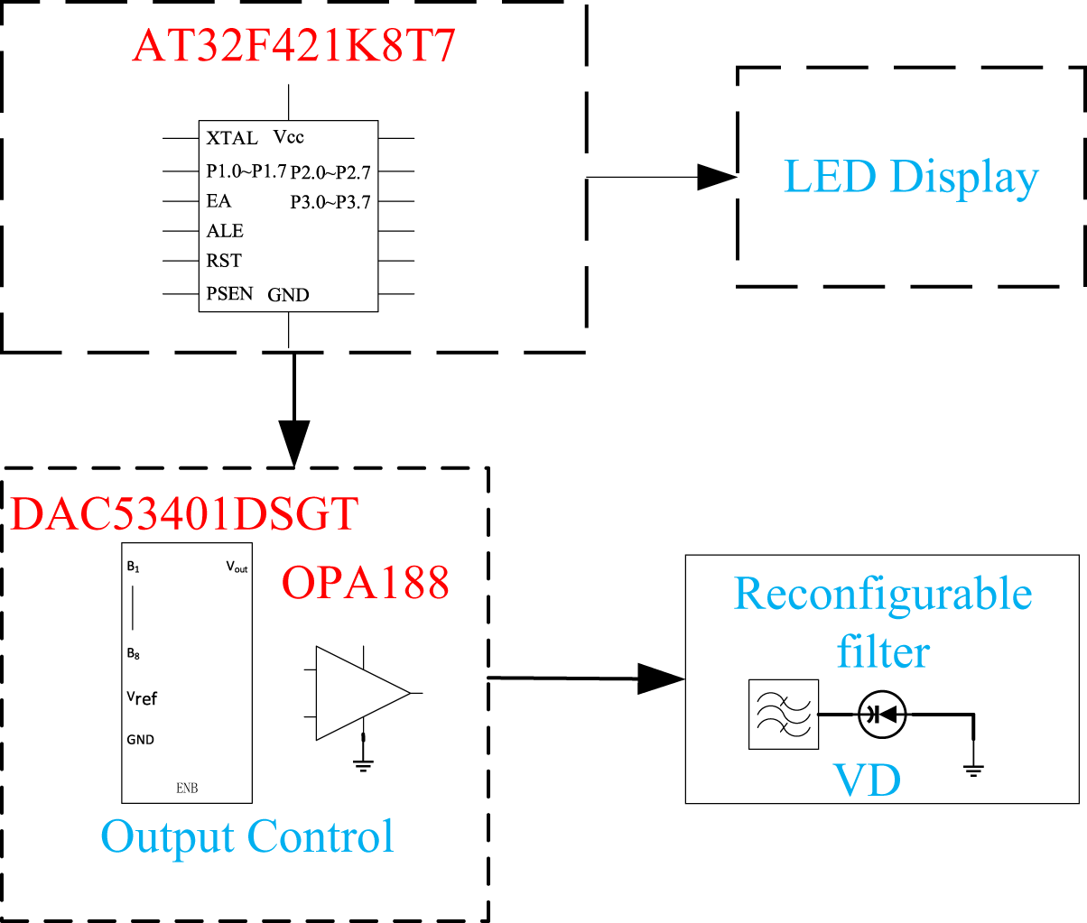
The capacitance of the varactor diode is changed by varying the voltage applied to its terminals. To enable more convenient voltage control, a controllable DC regulated power supply is applied. This system employs a microcontroller to manage the output voltage, dynamically adjusting the bias voltage at the varactor diode, as shown in Figure 5. By altering the junction capacitance of the varactor diode, it enables the reconfiguration of the filter. Figure 7 illustrates the block diagram of the control system, where the microcontroller manages the analog voltage output from the digital-to-analog converter (DAC) module. The output is then delivered to the varactor diode terminals via an operational amplifier and a voltage stabilization module. The four varactor diodes are controlled by the same bias voltage, and the control voltage is varied in increments of 0.1 V, enabling continuous tuning.
Basic modules of the power supply system.

Test results and analyses
The test experiment of the reconfigurable filter is carried out, fabricated on a Rogers 4350 substrate with a relative dielectric constant of 3.66, a loss tangent of 0.004, and a thickness of 0.762 mm. The circuit dimensions are 60 mm × 30 mm (0.60λ 0 × 0.30λ 0), where λ 0 is the free-space wavelength at the center frequency of 3 GHz. The physical prototype of the filter is shown in Figure 8(a), and the comparison of S 21 and S 11 between the measured and simulated results is provided in Figure 8(b) and (c), respectively, demonstrating good agreement.
As seen from Figure 8(b), the in-band insertion loss is less than 1 dB, with a reduction of approximately 0.3 dB compared to the simulation. The return loss within the operating band is below 12 dB in Figure 8(c), showing a deviation of 3–6 dB from the simulated values, primarily due to processing tolerances and variations in the characteristics of the varactor diode. The bandpass filter with reconfigurable band traps exhibits a trap bandwidth of approximately 150 MHz, a trap depth exceeding 13 dB, and a linear variation of the trap center frequency from 2.1 to 3.0 GHz, providing a tunable range of 900 MHz. In this configuration, the varactor diode is identified as the principal governing factor influencing the notch depth. As established by the equation (9):
 \begin{equation}
{Q}=\frac{1}{{\omega}{R_s}{C_j}},
\end{equation}
(a) Filter test setup, (b) Measurement and simulation S21, and (c) measurement and simulation S11 (solid line is simulation result, dashed line is test result).

where ω denotes the operating frequency, Rs represents the series resistance, and Cj represents the junction capacitance. The Q-factor of a varactor diode is predominantly influenced by its operating frequency and junction capacitance. In the circuit design presented in this study, the variation magnitude of the diode’s junction capacitance (0.35–3.2pF) exceeds that of the frequency variation (2.1–3GHz). Consequently, the dominant influencing factor is identified as the junction capacitance of the varactor diode. As the junction capacitance increases, the Q-factor exhibits a gradual reduction. Within the circuit implementation, the varactor’s capacitance progressively decreases from low-frequency to high-frequency operation. This characteristic corresponds to the observed trend in the graph where notch depth progressively intensifies, indicating enhanced suppression performance of the filter. The gradual deepening of the notch depth directly correlates with the strengthening of the filter’s rejection capability across the operational bandwidth. The measured center frequency deviates by around 150 MHz from the simulated value when the varactor diode is biased at zero, attributed to discrepancies between the actual diode characteristics and the datasheet specifications. At 4.8 GHz, the measured suppression exceeds 50 dB, demonstrating robust performance.
Table 3 is the comparison of the proposed reconfigurable notch-bandpass filter’s performance with other filters reported in the literature. Compared to existing techniques, the proposed filter offers a superior tunable range, with a minimum insertion loss of approximately 0.32 dB, and passband in-band insertion losses are all below 1 dB. Compared to other reported filters, the filter proposed in this work exhibits superior passband insertion loss. However, it shows relatively poorer stopband attenuation performance when compared to the filters presented in [Reference Zhang, Chan, Xue and Hu1, Reference Ebrahimi, Baum, Scott and Ghorbani6, Reference Smari, Dakhli, Fourn, Choubani and Sup22]. In addition, the tunable bandwidth range of the proposed bandpass filter with notch functionality is narrower than that reported in [Reference Ebrahimi, Baum, Scott and Ghorbani6, Reference Song, Chen, Patience, Chen, Iman and Fan19], and further improvement is needed in this aspect. Regarding physical dimensions, the overall size of the proposed design also requires optimization.
Comparison of bandpass filters with reconfigurable band traps and tunable bandstop filters

a Stopband rejection.
b Varactor diode-coupled resonator.
c PIN diode-coupled resonator.
d Capacitively loaded loops.
Conclusion
In this article, an S-band bandpass filter with wide reconfigurable transmission zeros is presented. The main transmission path consists of two stepped impedance resonators, coupled with four reconfigurable structures to enable trap frequency reconfiguration. This design provides improved in-band performance and enhanced stopband characteristics, achieving a reconfigurable bandwidth of approximately 900 MHz. The proposed filter system allows for trap frequency selection within the 2.1 to 3 GHz range, offering a tuning range of around 900 MHz, making it highly valuable for various applications. As a highly flexible and adaptive RF front-end component, the reconfigurable notch-bandpass filter is particularly well-suited for future communication and sensing systems characterized by highly dynamic spectrum environments, system heterogeneity, and complex interference scenarios. It serves as a key module in satellite communications, aerospace systems, and wireless communication networks. And we will further refine the filter by enhancing its performance in terms of miniaturization and improved suppression capability.
Data availability statement
The data used in this research work are available from the authors by reasonably request.
Competing interests
The authors declare no competing interests.
Notation
The symbols used throughout the paper are shown in Table 4.
List of symbols used in this paper.


Mi Lin received her M.S. degree in 2004 and Ph.D. degree in circuit and system from Zhejiang University, Hangzhou, China, in 2010, and joined Hangzhou Dianzi University (HDU) since 2004. She is currently an associate professor in the School of Electronics and Information at Hangzhou Dianzi University. Her major research interests include RF microwave circuits, wireless communication.

Tong Zhou received the B.E. degree from the Anhui Normal University, Wuhu, China, in 2023. He is currently pursuing the M.S. degree with Hangzhou Dianzi University, Hangzhou, China. His current research interests include the design of microwave devices and power amplifiers.

Guohua Liu received the M.S. degree from East China Normal Uni- versity, Shanghai, China, in 2004, and the Ph.D. degree in electronic science and tech- nology from Hangzhou Dianzi University, Hangzhou, China, in 2020. He is currently a Professor with the School of Electronics and Information, HDU. His current research interests include microwave and RF circuits, sensors, antennas, and wireless com- munication systems design.