Introduction
Diffusion barrier plays an important role and is extensively studied and applied in the fields of integrated circuit (IC) [Reference Holloway and Fryer1, Reference Nakano, Itabashi and Akahoshi2, Reference Qu, Tan, Zhou, Chen, Xie, Ru and Li3, Reference Civale, Croes, Miyamori, Velenis, Redolfi, Thangaraju, Van Ammel, Cherman, Van der Plas, Cockburn, Gravey, Kumar, Cao, Travaly, Tökei, Beyne and Swinnen4], fuel cell [Reference Brandner, Bram, Jan, Buchkremer and Stöver5, Reference Maric, Neagu and Zhang-Steenwinkel6, Reference Lee, Park and Hong7], high-temperature protective films [Reference Haynes, Zhang, Cooley, Walker, Reeves and Pint8, Reference Wang, Guo and Peng9, Reference Joly, Brun and Lacombe10], thermoelectric (TE) power generation [Reference Zhao, Li, He, Jiang and Chen11, Reference Hsu, Cheng, Chiou, Huang, Liu, Lin, Chao, Yang, Chang and Cheng12, Reference Gu, Bai, Xia, Huang, Li, Shi and Chen13, Reference Hsieh, Wang, Lin, Chakroborty, Lee, Chu and Wu14], etc. The main purpose of a diffusion barrier is to effectively control the interdiffusion between two different materials such as substrate and interconnect (or electrode). Therefore, the interfacial stability, such as that of the bonding strength and the thermal and/or electrical contacting, can be considerably enhanced. As a result, the reliability or service behavior of corresponding devices is ensured.
Using the Seebeck effect, TE modules produce electrical power when charge carriers move from the hot side to the cold side of TE materials under a temperature difference [Reference Rowe15]. During practical service, the temperature of the hot side of a TE element, which is the key component of the TE module and is made up of electrode and TE material, is usually as high as hundreds of degrees centigrade. Great efforts have been made to protect the hot-side TE materials from sublimation at high temperature [Reference Brostow, Datashvili, Hagg Lobland, Hilbig, Su, Vinado and White16, Reference Brostow, Chen and White17, Reference Saber and El-Genk18, Reference Dong, Li, Tang, Zou, Huang, Zhou, Jiang, Zhang and Chen19]. At the same time, diffusion barrier is imperative and has great influence on the structure reliability and performance stability of the TE devices [Reference El-Genk and Saber20]. In most cases, there are initiative and uncontrollable interdiffusions at the interface between the hot-side electrode and the TE material, which generally introduces complicated intermetallic compounds (IMCs) and then degrades the interfacial bonding strength and electrical properties. As a result of long time service, the performance and stability of the TE element and consequently those of the TE device will be considerably deteriorated.
Currently, the developing of diffusion barrier follows a traditional process. First, select a number of barrier material candidates based on some general principles, including electric and thermal conductivities, melting points, and the coefficient of linear thermal expansion (CLTE). Second, synthesize samples to obtain macrointerfaces, usually in the size of several millimeters, between the substrate material and each of the barrier material candidates. Third, age each of the macrointerface in an accelerated way, and then investigate the thickness of the interfacial diffusion layer and related transport properties such as the bonding/shear strength and the interfacial contact resistivity. Finally, evaluate the interfacial structure reliability and performance stability for different barrier candidates, and identify the preferred diffusion barrier material. It is clear that the above four steps form a serial and full screening process.
In some fields, such as the IC, the above traditional way of developing barrier material is acceptable. First, the substrate and interconnect materials, usually Si (or corresponding oxides) and Cu, respectively, are with simple composition and crystal structure. Their chemical and physical properties have been fully studied. So under the guidance of existing theories, limited amount of barrier layer candidates can be effectively identified before detailed experimental study. Second, the substrate and electrode materials have remained roughly unchanged for over fifty years, which makes it acceptable for long-term screening and optimization of the barrier layer materials. Third, IC technology hosts a huge market and a large amount of profits, so it is tolerant to costly and time-consuming research of corresponding diffusion barrier materials.
In the field of TE power generation, however, the situation is quite different. First, there are various families of TE materials, for example, silicides [Reference Joshi, Lee, Lan, Wang, Zhu, Wang, Gould, Cuff, Tang, Dresselhaus, Chen and Ren21], half-Heuslers [Reference Appel, Zilber, Kalabukhov, Beerib and Gelbstein22], and tellurides of Bi [Reference Sumithra, Takas, Misra, Nolting, Poudeu and Stokes23] and Pb [Reference Gelbstein24]. Meanwhile, the compositions and crystal structures of most TE materials are complicated, which makes it very difficult to effectively identify preferred barrier layer materials by predicting diffusion behaviors at the interface between the barrier material candidates and the TE substrate with existing theories. Currently, the common practice is to try one by one from a pool of barrier material candidates through experiments. Second, trying of each barrier layer candidate is usually costly and time-consuming because it is difficult to obtain a qualified interface between a TE substrate and a barrier material candidate, on which evaluation of the effectiveness of the diffusion barrier is based. The reason is that the current TE materials are generally brittle and are with weak mechanical strength, whereas their CLTE is usually much higher than that of widely used barrier layer materials such as W and Ta, which makes it difficult and sometimes impossible to fabricate a strong and crack-free interface for further evaluation. Third, unlike the fully commercialized IC technology, the TE technology, though has a good potential for special power supplying and waste heat harvesting, currently lacks sufficient market and profit. As a result, the high cost and low efficiency in the development of the diffusion barrier materials are hard to be accepted by most TE researchers, which in turn explains why the development of the barrier materials and TE modules lags far behind that of the TE materials.
TE devices are expected to work stably for years or even longer; therefore, qualified diffusion barrier material is indispensable to the practical application of a TE device. At the same time, under the guidance of improved TE theories and with optimized fabrication instruments, nowadays new TE materials with enhanced TE properties are developed at accelerated speeds [Reference Liu, Shi, Xu, Zhang, Zhang, Chen, Li, Uher, Day and Jeffrey Snyder25, Reference Jiang, Qiu, Chen, Zhang, Zhao, Ren, Shi and Chen26]. Practical applications of these newly developed TE materials also call for high-efficiency development of corresponding TE modules, among them is one of the key issues of the diffusion barrier materials.
In recent years, Materials Genome Initiative makes the development of new materials faster and more efficient. Under the guidance of a high-throughput strategy, in this article, we developed a high-efficiency screening method of interfacial diffusion barrier materials for TE modules. The key point that restricts the developing of the barrier materials is the costly and time-consuming fabrication processing of TE elements with the sandwich structure of “electrode/barrier material/TE material” to obtain qualified interface of millimeter scale between the TE substrate and barrier material candidates. In this article, we bypassed the fabrication processing of the qualified interface of millimeter scale by cosintering the mixed powders of TE substrate material and various barrier material candidates in one step. As a result, a number of interfaces of micrometer scale were simultaneously obtained in one single sample. Based on the resulting sample with various interfaces of micrometer scale between barrier material candidates and the TE material substrate, diffusion layer characterizations and accelerated aging were conducted, and the preferred barrier material was screened out efficiently.
Results and discussion
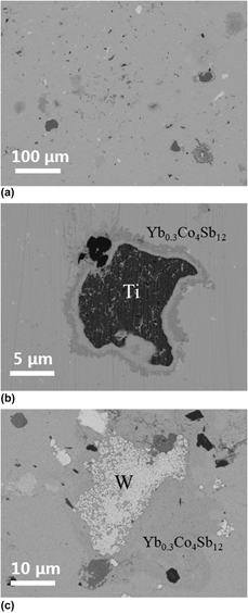
Figure 1(a) is a low multiplier SEM photograph of the as sintered sample with Yb0.3Co4Sb12 as the TE substrate and particles of 9 kinds of barrier material candidates dispersing in it. Combining the composition analysis with EDS, it is easy to identify different interfaces of millimeter scale between the Yb0.3Co4Sb12 substrate and particles of individual barrier material candidates. Figures 1(b) and 1(c), as two examples, show the high multiplier SEM photographs of the typical as sintered Ti/Yb0.3Co4Sb12 and W/Yb0.3Co4Sb12 interfaces, respectively. It is found that regardless the great differences of densification temperature and CLTE between Yb0.3Co4Sb12 and W, the corresponding interfaces of micrometer scale are strongly bonded and crack-free. This is because the W particles are small in size, which helps to avoid high interfacial stress from CLTE mismatch. Besides, the shapes of the W particles are irregular, which also helps to disperse and absorb the interfacial stress. Based on the above results, it is concluded that cosintering of mixed powders of Yb0.3Co4Sb12 substrate and diffusion barrier material candidates is an effective way to achieve strong and crack-free interfaces. This makes it possible to further study the interfacial diffusion behavior and compare the effectiveness of various barrier material candidates based on the interfaces of micrometer scale.
(a) SEM photograph of the as sintered sample with Yb0.3Co4Sb12 as the substrate and particles of Ti, Zr, Hf, V, Nb, Ta, Cr, Mo, and W dispersing in it. (b) Microstructure at a typical Ti/Yb0.3Co4Sb12 interface. (c) Microstructure at a typical W/Yb0.3Co4Sb12 interface.

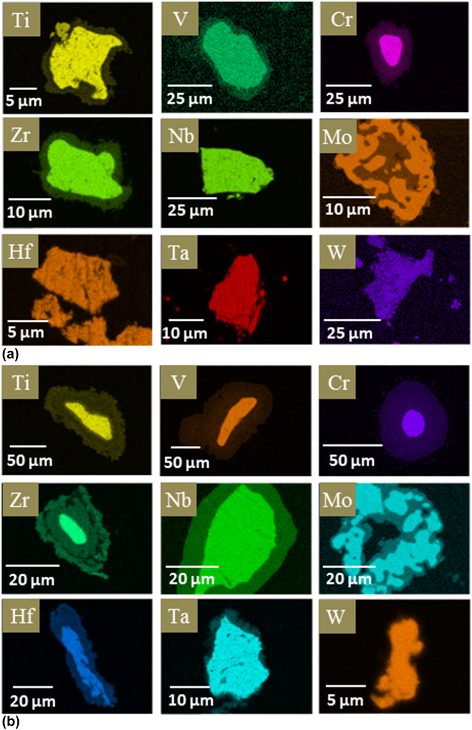
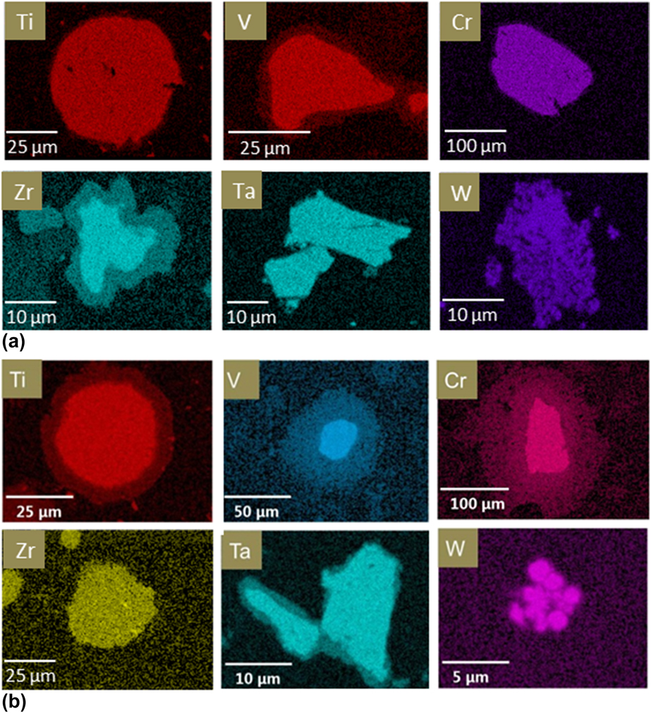
Figure 2(a) shows the mapping results of the typical as sintered interfaces between the Yb0.3Co4Sb12 substrate and the particles of 9 kinds of barrier candidates. Based on Fig. 2(a), the thickness of the interfacial diffusion layer at different kinds of interfaces is easy to be measured.
Mapping results of typical interfaces between the Yb0.3Co4Sb12 substrate and particles of different barrier layer candidates (a) before and (b) after aging at 650 °C for 2 days in vacuum.
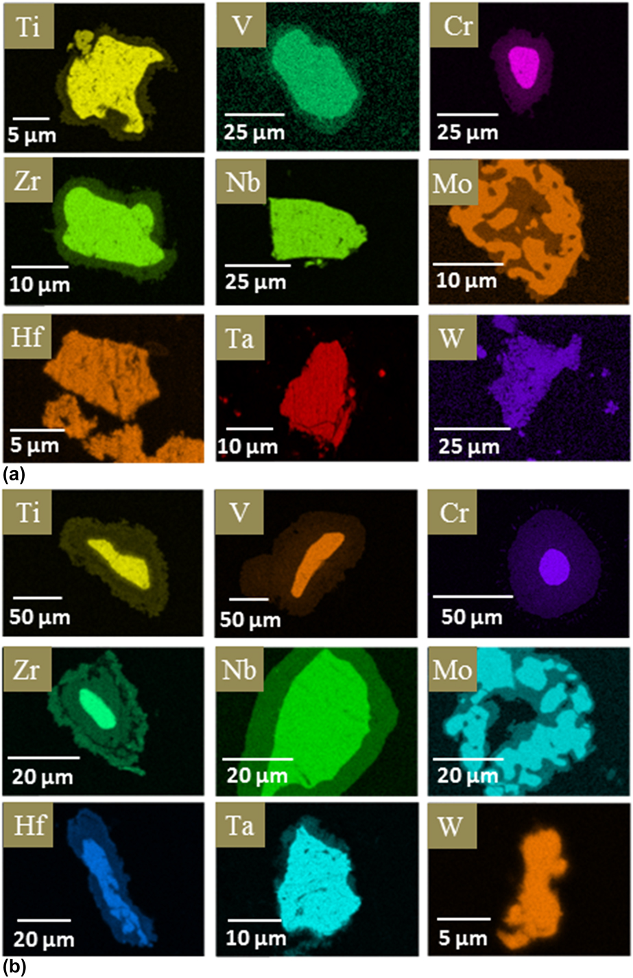
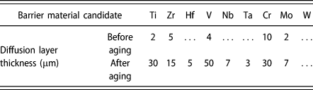
After being aged at 650 °C for 2 days in vacuum, interfacial diffusion layers grow thicker at different kinds of interfaces. Figure 2(b) shows the element mapping results of the typical aged interfaces between the substrate and various barrier material particles. For each barrier material candidate before and after aging, five interfaces at different random positions in sample matrix were selected, and the thickness of corresponding newly formed diffusion layers was estimated. Table I presents the average diffusion layer thickness at various interfaces for each barrier candidate. It is clear that after aging, the interfacial diffusion at W/Yb0.3Co4Sb12 interface is neglectable, and the thickness of the interfacial diffusion layer at the Ta/Yb0.3Co4Sb12 interface is only about 3 μm. This is reasonable considering the excellent high-temperature chemical stability of W and Ta as well as their high melting points. At the Mo/Yb0.3Co4Sb12, Nb/Yb0.3Co4Sb12, and Hf/Yb0.3Co4Sb12 interfaces, the thickness of the interfacial diffusion layers becomes a little thicker but less than 10 μm. While at the Ti/Yb0.3Co4Sb12, Zr/Yb0.3Co4Sb12, V/Yb0.3Co4Sb12, and Cr/Yb0.3Co4Sb12 interfaces, the interfacial diffusion layers are much more thicker and all above 15 μm, which is related to higher chemical activities and relatively lower melting points of the above barrier candidates.
Average diffusion layer thickness at the interfaces between Yb0.3Co4Sb12 substrate and particles of different barrier material candidates before and after being aged at 650 °C for 2 days in vacuum.

Though W and Ta demonstrate an excellent ability to inhibit interfacial diffusion, they are not preferred barrier layers for Yb0.3Co4Sb12 substrate when it comes to interfaces of millimeter scale in TE modules. The reason is that chemically they are too inert to form strong bonding with Yb0.3Co4Sb12 substrate and physically their CLTEs (W: ∼4.6 × 10⁻⁶ K−1, Ta: ∼6.6 × 10⁻⁶ K−1 at room temperature) are much lower than that of Yb0.3Co4Sb12 (∼9.5 × 10⁻⁶ K−1 at room temperature), which makes it almost impossible to fabricate W/Yb0.3Co4Sb12 or Ta/Yb0.3Co4Sb12 joint with strong and crack-free interfaces. At the same time, from the economic point of view, W, Ta, and Hf are too expensive for large-scale applications. As a result, Nb and Mo were screened out as potential diffusion barrier materials for Yb0.3Co4Sb12 substrate.
To evaluate the screen results and verify the interfacial stability, we selected Mo as the barrier layer and fabricated Mo/Yb0.3Co4Sb12 TE elements. For comparison, TE elements with Ti/Yb0.3Co4Sb12 interface of millimeter scale were also fabricated.
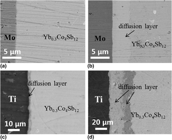
Figures 3(a)–3(d) show the microstructures of Mo/Yb0.3Co4Sb12 and Ti/Yb0.3Co4Sb12 interfaces before and after aging at 650 °C for 2 days, respectively. After sintering and before accelerated aging, the initial interdiffusion at the Mo/Yb0.3Co4Sb12 interface is neglectable, and the diffusion layer thickness at the Ti/Yb0.3Co4Sb12 interface is about 2 μm. Prolonging the aging time, the interfacial diffusion layer at the Mo/Yb0.3Co4Sb12 interface grows evidently more slowly than that at the Ti/Yb0.3Co4Sb12 interface. As a result, the thickness of the interfacial diffusion layer at the Mo/Yb0.3Co4Sb12 and Ti/Yb0.3Co4Sb12 interfaces reaches about 5 μm and 34 μm after 2 days aging at 650 °C, respectively. This roughly agrees with the data in Table I, which was obtained through the high-efficiency screening method. Based on the above results, it is concluded that in terms of the thickness of the interfacial diffusion layer, the screening result of the barrier materials candidates based on the interfaces of micrometer scale between Yb0.3Co4Sb12 substrate and barrier material particles in the cosintered samples is applicable for the interfaces of millimeter scale between Yb0.3Co4Sb12 substrate and barrier candidates in the practical fabricated TE elements or TE modules.
Microstructure of the Mo/Yb0.3Co4Sb12 and Ti/Yb0.3Co4Sb12 interfaces of millimeter scale before and after aging at 650 °C for 2 days in vacuum. (a) Mo/Yb0.3Co4Sb12, before aging. (b) Mo/Yb0.3Co4Sb12, after aging. (c) Ti/Yb0.3Co4Sb12, before aging. (d) Ti/Yb0.3Co4Sb12, after aging.

Besides constrained interfacial diffusion, it is also required that the electrical resistivity at the interface between the TE substrate and preferred barrier material be low and stable after aging. We then measured the interfacial resistivity at the Mo/Yb0.3Co4Sb12 and Ti/Yb0.3Co4Sb12 interfaces of millimeter scale before and after aging. It is found that the initial interfacial resistivity at the Mo/Yb0.3Co4Sb12 and Ti/Yb0.3Co4Sb12 interfaces is about 3 and 5 μΩ cm2, respectively. After being aged at 650 °C for 2 days, the interfacial resistivity at corresponding interfaces rises up to 7 and 20 μΩ cm2, respectively. This indicates that the interfacial resistivity is largely influenced by the interfacial diffusion, and it is further confirmed that Mo is a preferred diffusion barrier material for Yb0.3Co4Sb12 substrate.
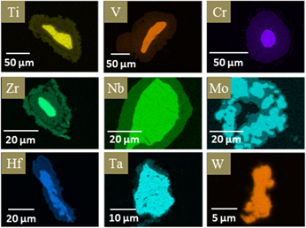
The above high-efficiency screening method of diffusion barrier materials using cosintering method is also suitable for p-type skutterudites. Figures 4(a) and 4(b) are the element mapping results of the typical interfaces of micrometer scale between the CeFe4Sb12 substrate and particles of various barrier material candidates before and after aging at 600 °C for 2 days in vacuum, respectively. According to Fig. 4(b), during aging, similar with that in the case of the n-type Yb0.3Co4Sb12 substrate, the interdiffusion at the W/CeFe4Sb12 and Ta/CeFe4Sb12 interfaces are well constrained. This verifies that W and Ta are generally good barrier materials for many different substrates in terms of constraining interdiffusion alone. The diffusion layers at the Cr/CeFe4Sb12 and V/CeFe4Sb12 interfaces are quite thick, indicating that Cr and V are not qualified barrier layer materials for CeFe4Sb12 substrate. At the aged Ti/CeFe4Sb12 interface, an evident while comparatively thin diffusion layer is observed. One thing worth mentioning is that the diffusion layer at the Zr/CeFe4Sb12 interface grows so fast that after aging the whole Zr particle was reacted with CeFe4Sb12 substrate and tuned into ZrSb2.
Mapping results of typical interfaces between the CeFe4Sb12 substrate and particles of different barrier material candidates (a) before and (b) after aging at 650 °C for 2 days in vacuum.

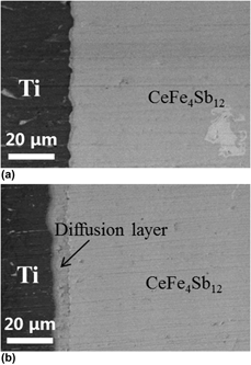
Based on the above results, it is found that W, Ta, and Ti are much better candidates than Cr, V, and Zr as the barrier materials for CeFe4Sb12 substrate. Take into account that Ti is cheaper and has more matched CLTE to CeFe4Sb12 substrate than W and Ta, Ti was screened out as the preferred barrier candidate for CeFe4Sb12 substrate. Like in the case of the n-type Yb0.3Co4Sb12 skutterudite, corresponding TE elements were then fabricated and aged, and the interfacial diffusion of the Ti/CeFe4Sb12 interface of millimeter scale was investigated. As are shown in Figs. 5(a) and 5(b), under the same aging condition, the thickness of the interfacial diffusion layer at the Ti/CeFe4Sb12 interface of TE elements roughly agrees with that at the Ti/CeFe4Sb12 interface in cosintered samples.
Microstructure of the Ti/CeFe4Sb12 interface of millimeter scale (a) before and (b) after aging at 650 °C for 2 days in vacuum.

Essentially, the high-efficiency screening of interfacial diffusion barrier materials developed in this article is based on the interfaces of micrometer scale between expected TE substrate and particles of barrier material candidates. As most TE materials and potential barrier candidates including metal elements and various alloys can be obtained in the form of powder, there is little difficulty in fabricating desired interfaces by cosintering of corresponding powders. As a result, the above high-efficiency screening method has great potential to be applied in various TE materials and to help promote the developing of TE modules. Moreover, it can also be applied in other technological fields such as high-temperature protective films and fuel cells.
Conclusions
In this article, using a high-throughput strategy, we developed a high-efficiency method to screen out preferred barrier materials from various candidates for TE modules. By cosintering the mixture of TE substrate powder and particles of various barrier material candidates, we obtained simultaneously interfaces of micrometer scale between the TE substrate and various barrier material candidates and integrated them into a single sample. Parallel aging and microstructure characterization were then conducted for various interfaces simply based on the same sample. By identifying and comparing the thickness of the interfacial diffusion layers at different kinds of interfaces before and after aging, preferred barrier materials were swiftly screened out for corresponding TE substrates. In this article, the effectiveness of this high-efficiency screening method was testified on n-type Yb0.3Co4Sb12 and p-type CeFe4Sb12 skutterudites. Mo and Ti were screened out as the preferred barrier materials, respectively. This method bypasses the complicated processing optimizations of the sandwich structured TE element of “electrode/barrier material/TE material” for each barrier material candidate in the traditional way to obtain interface of millimeter scale before the screening of barrier material candidates. As a result, the screening of the barrier materials for TE devices becomes much more efficient and economical.
Materials and methods
In this article, Yb0.3Co4Sb12 and CeFe4Sb12, the widely studied n-type and p-type filled skutterudites, were selected as the TE substrate materials to show in detail how the high-efficiency screening method of diffusion barrier materials was conducted.
Take into consideration that the preferred interfacial diffusion barrier material for TE modules should itself be with good electrical and thermal conductivities and its melting point should be well above the TE module’s hot-side working temperature, 9 metal elements of Ti, Zr, Hf, V, Nb, Ta, Cr, Mo, and W (Alfa Aesar, Ward Hill, MA) were selected as the barrier material candidates for Yb0.3Co4Sb12 and 6 metal elements of Ti, Zr, V, Ta, Cr, and W (Alfa Aesar, Ward Hill, MA) were selected as the barrier material candidates for CeFe4Sb12. We weighed the powders of Yb0.3Co4Sb12 and CeFe4Sb12 substrate materials as well as those of the barrier material candidates individually. Each of the powders of the barrier material candidates takes up about 0.5 wt% of that of corresponding TE substrate material. The particle sizes of the TE substrate material are under 95 μm. The particle sizes of the above barrier material candidates are less than 150 μm, and their purities are no less than 99.9%. The powders were then manually mixed to make the barrier material candidates disperse uniformly in the TE substrates. The mixed particles were then loaded into a graphite die with 12.7 mm in diameter for spark plasma sintering.
The syntheses of the Yb0.3Co4Sb12 and CeFe4Sb12 powders followed the same processes described in Refs. Reference Zhao, Shi, Chen, Zhang, Zhang and Pei27 and Reference Tang, Chen, Goto and Hirai28, respectively. The sintering parameters of the samples with Yb0.3Co4Sb12 and CeFe4Sb12 as the substrate materials are the same as those described in Refs. Reference Gu, Bai, Xia, Huang, Li, Shi and Chen13 and Reference Sumithra, Takas, Misra, Nolting, Poudeu and Stokes23, respectively. The surfaces of the as sintered samples were then manually polished with silicon carbide sand papers (5000 mesh). The microstructure and chemical composition around the resulting interfaces between the barrier material particles and corresponding TE substrate were investigated through scanning electronic microscope (SEM; ZEISS, SUPRA-55-SAPPHIRE, Oberkochen, Germany) and energy dispersive spectrometer (EDS; OXFORD, X-MaxN, Cambridge, U.K.). For skutterudite TE modules, the typical hot-side service temperature is about 550 °C, so the sintered samples with n-type and p-type TE substrates were aged at 650 and 600 °C, respectively, in vacuum for 2 days to accelerate the interdiffusion around the interfaces between the barrier material particles and corresponding TE substrate. After aging, the microstructure and chemical composition at the interfaces were investigated again. Finally, by comparing the thickness of the newly formed diffusion layer at different interfaces, preferred diffusion barrier candidate was screened out.
For further confirmation, after the above high-efficiency screening process, TE elements with preferred barrier material were fabricated with optimized synthesizing parameters through the traditional one-step sintering process. Bulks of 3 × 3 × 5 mm (H) with qualified crack-free interface were cut for accelerated aging in vacuum. The diffusion layer thickness at the aged interfaces of millimeter scale was investigated for comparison with that at the aged interfaces of micrometer scale. Meanwhile, the contact resistivity of the interface of millimeter scale was measured on the home-made four probe platform mentioned in Ref. Reference Gu, Xia, Huang, Bai, Li and Chen29.
Acknowledgment
This work was financially supported by the National Key Research and Development Program of China (Contract No. 2018YFB0703600) and National Natural Science Foundation of China (Contract Nos. 51572282 and 51632010).