Introduction
Hard disk drives (HDDs) and USB flash memories are the core components in computers that are used to store data. These memory devices are nonvolatile. The storage data in the world’s computers and servers continue to increase, consuming large amounts of energy to access the servers. Computing and analysis using big data especially require huge storage memories with high-speed access. However, present HDDs and flash USB have fatal issues related to access speed. “Storage-class memory (SCM)” has been proposed to overcome these issues.Reference Bull, Kurdi, Scott, Lam, Gopalakrishnan and Shenoy1 Although magnetoresistance random-access memory (MRAM),Reference Ando, Fujita, Yuasa, Suzuki, Nakatani, Miyazaki and Yoda2 phase-change RAM (PC-RAM),Reference Ielmini and Lacaita3 resistance change RAM,Reference Waser4 and ferroelectric RAMReference Jameson, Gilbert, Koushan, Saenz, Wang, Hollimer and Kozicki5 have been explored thus far, since 2017, PC-RAM has been the leader with the launch of the device Optane by Intel and Micron Technology.6
The memory mechanism of PC-RAM is simple, relying on an amorphous to crystal phase transition in a Ge-Sb-Te chalcogenide alloy that produces a three orders of magnitude electric resistance change.Reference Wuttig7 The alloy was invented in the late 1980s by Panasonic,Reference Yamada, Ohno, Akahira, Nishiuchi, Nagata and Takao8,Reference Yamada, Ohno, Nishiuchi, Akahira and Takao9 and it was first commercialized as a nonvolatile recording film in rewriteable optical discs (DVD and Blu-ray) in the 1990s. The Ge2Sb2Te5 composition shows the best performance for write-erase durability, large optical contrast (refractive index), and switching speed.Reference Raoux and Wuttig10 Due to its excellent performance and success in optical memory, the alloy was soon applied to electric resistive memory because of its large resistance contrast between the amorphous and crystal states.
Development of interfacial phase-change memory
One area of needed improvement in PC-RAM is the current relatively low efficiency of switching energy consumption compared with competitive devices. The recording and erasing mechanism in PC-RAM is simple. For the Ge-Sb-Te alloy, the difference in electric resistance values between the amorphous (high) and crystalline (low) states is large (three orders magnitude). The crystalline and amorphous states are called SET and RESET, respectively. The phase transitions from SET to RESET and from RESET to SET are carried out by injecting an electric current high and low for a certain length of time. In the transition from SET to RESET, the Ge-Sb-Te alloy needs to be heated to the melting point (>930 K), followed by a rapid quench to form an amorphous state, whereas the reverse transition needs to be heated to the crystallization temperature (∼430 K). Therefore, this RESET process consumes relatively high Joule heating energy.Reference Raoux and Wuttig10
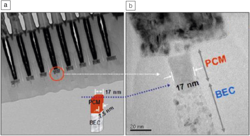
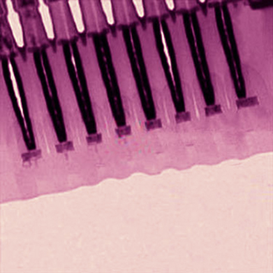
To reduce the energy consumption, several thermal-management technologies have been proposed, and adoption of a low thermal conductive protection layer adjacent to the memory cell has been implemented.Reference Russo, Ielmini, Redaelli and Lacaita11 From the first law of thermodynamics, the smaller the melting portion, the lower the Joule heating energy. Therefore, recently reported memory cell size has been designed to be less than a few tens of nanometers, as shown in Figure 1.Reference Lee, Park, Cho, Park, Bae, Park, Park, An, Bae, Ahn, Kim, Horii, Song, Shin, Park, Kim, Chung, Moon and Ryu12,Reference Kim, Cho, Im, Cho, Kim, Oh, Ahn, Park, Nam, Moon and Chung13
Cross-sectional transmission electron micrograph of 7.5-nm (width) × 17-nm (length) confined phase-change memory cells. (a) Array of memory cells, and (b) zoomed-in view of a single cell. Note: PCM, Ge-Sb-Te alloy phase-change film; BEC, bottom electric contact. Reprinted with permission from Reference Reference Kim, Cho, Im, Cho, Kim, Oh, Ahn, Park, Nam, Moon and Chung13. © 2010 IEEE.

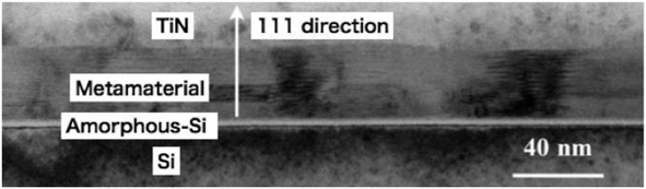
An alternative solution to overcome the issue is to use the second law of thermodynamics—reducing entropic energy loss in switching.Reference Tominaga, Wang, Kolobov and Fons14 After discovering that the large electric resistance change in Ge-Sb-Te alloys relies on the bonding states (octahedral or tetrahedral) of Ge and Te atoms,Reference Kolobov, Fons, Frenkel, Ankudinov, Tominaga and Uruga15 a nonmelting switching model was proposed.Reference Tominaga, Fons, Kolobov, Shima, Chong, Zhao, Lee and Shi16 Experimental fabrication of the engineered materials was started in 2008.Reference Tominaga, Simpson, Fons and Kolobov17 The metamaterial has to be designed from a superlattice, in which GeTe layers and Sb2Te3 layers are alternately stacked as shown in Figure 2. By exchanging the positions of Ge atoms with adjacent Te atoms in the GeTe bilayers, the resistance change is attained. It should be noted that the Sb2Te3 layers do not take part in the phase transition or resistance change, and only provide a scaffold for the Ge position switching. The device performance of the superlattice-PC-RAM composed of a GeTe/Sb2Te3 multilayer was first reported in 2011, and a reduction of the RESET switching energy by 90% was demonstrated.Reference Simpson, Fons, Kolobov, Fukaya, Krbal, Yagi and Tominaga18 The superlattice-PC-RAM has been called interfacial phase-change memory (iPCM). However, it was discovered that iPCM has another feature related to the topological state in quantum mechanics (described next).Reference Sa, Zhou, Sun, Tominaga and Ahuja19
Metamaterial (superlattice) film composed of [(GeTe)2(Sb2Te3)1]20 blocks deposited on a Si wafer under a stress-free condition.Reference Tominaga, Simpson, Fons and Kolobov17

Topological insulator and chalcogenide crystals
A topological insulator (TI) is an insulator in the bulk state, with a current that can flow along the edges or surfacesReference Hasan and Kane20–Reference Ando22 and have a special conductive state. The unusual behavior of the TI is attributed to the topological nature of the electronic bandgap.Reference Xiao, Chang and Niu23 In insulators with significantly large spin–orbit interaction (SOI), the lowest conduction band and the uppermost valence band may be reversed by the energy due to SOI.Reference Bernevig, Hughes and Zhang24 Although normal insulators (NIs) usually have a bandgap with or without SOI, insulators with reversed bands by SOI are different from NIs in topology. When the TI and NI electronic bands touch due to the TI surface contacting the NI surface, the wave functions (Bloch wave) from the TI and NI must combine at the interface to create new electronic band structures. In this case, two topologically different bandgaps must be tied together at the interface. The wave functions from the TI tunnel to the NI side across the interface, but the transmitted wave functions inside the NI are not influenced by the SOI energy. Therefore, the inverted bands return to a normal bandgap in a NI.
The NI wave functions that tunneled into the TI undergo SOI, and band inversion thereby occurs. The only way to accommodate these two different twisted bandgaps is to close the bandgap once at the interface using a linear dispersion connection band (called Dirac cone) between the valence band top and conduction band bottom. Here, notice that a NI is not limited to solids or liquids; even vacuum or air could be a good candidate for a NI. Therefore, the surface of a TI in vacuum or air is conductive.
Theoretical predictionsReference Fu and Kane25,Reference Zhang, Liu, Qi, Dai, Fang and Zhang26 followed by experimental confirmationsReference Xia, Qian, Hsieh, Wray, Pal, Lin, Bansil, Grauer, Hor, Cave and Hasan27–Reference Hsieh, Xia, Qian, Wray, Meier, Dil, Osterwalder, Patthey, Fedorov, Lin, Bansil, Grauer, Hor, Cava and Hasan29 have reported many chalcogenides as TIs.Reference Yang, Setyawan, Wang, Nardelli and Curtarolo30 The topological properties of Group V–VI type chalcogenides are tightly protected by both time reversal and spatial inversion symmetry, where the compounds are not magnetic and the crystal lattice has inversion symmetry. Among them, Bi2Se3, Bi2Te3, and Sb2Te3 are known as typical three-dimensional (3D) TIs,Reference Bernevig, Hughes and Zhang24 which have a surface conductive mode where electron scattering is greatly suppressed. It is interesting to note that these chalcogenides are composed of a five-atomic-layer unit called a quintuple layer (QL). QLs are weakly bonded by van der Waals forces through Te–Te bonds located at both outsides of QLs; for example, in Sb2Te3, one QL is made of a Te-Sb-Te-Sb-Te arranged layer (thickness = 1 nm). When the number of QLs is less than three, the top and bottom surface helical spin modes are coupled through the film thickness, losing the topological surface state.Reference Lu, Shan, Yao, Niu and Shen31,Reference Zhang, He, Chang, Song, Wang, Chen, Jia, Fang, Dai, Shan, Shen, Niu, Qi, Zhang, Ma and Xue32
Issues on the application of topological states to electronics devices
TIs have attracted much attention for future electronics device applications and quantum computing, however, several technical issues must be overcome. The first is that topological conductive channels only exist on the film surfaces (3D-TI) or the edges (2D-TI). As the bottom surface of a TI film contacts a substrate or an electrode, only one surface is available for passing a current in a 3D-TI film. The second is that since the conductive surface state is limited to a narrow thickness near the surface, applications to a transistor configuration will be challenging. The third is that TI films are usually obtained by the cleavage of a small single crystal, which is fabricated by chemical vapor deposition.Reference Zhang, He, Chang, Song, Wang, Chen, Jia, Fang, Dai, Shan, Shen, Niu, Qi, Zhang, Ma and Xue32 This technology cannot be easily transferred into a semiconductor production process. Nevertheless, a variety of TI devices have been recently proposed, including spin-control devices.Reference Xiu and Zhao33 However, almost all of the devices have only been operated at low temperatures (<10 K), which is not consistent with theoretical suggestions that TI protected states by the time-reversal and spatial-inversion symmetries are robust and can withstand thermal disturbances even at room temperature.
iPCM as topological insulators
The switching film in an iPCM device is composed of a superlattice of GeTe and Sb2Te3 sublayers, which are alternately stacked.Reference Simpson, Fons, Kolobov, Fukaya, Krbal, Yagi and Tominaga18 As previously mentioned, Sb2Te3 is a TI, whereas GeTe is a NI with a narrow bandgap.Reference Kolobov, Kim, Giussani, Fons, Tominaga, Calarco and Gruverman34 Thus, the superlattice has a repetitive structure of (TI/NI)n, where n is an integer. If the sublayers of NI and TI are thick enough, the bottom and top surface states of the adjacent TI-QLs cannot be hybridized.Reference Lu, Shan, Yao, Niu and Shen31 In this case, topologically protected states could be preserved in the bulk, that is, all the interfaces may become conductive channels as topologically protected states.
Also, a topological conductive mode appears on the top and bottom surfaces in the superlattice. Therefore, tuning each number of (TI/NI)n in an iPCM device enables control of the topological states.Reference Halasz and Balents35,Reference Tominaga, Kolobov, Fons, Nakano and Murakami36 The stacking freedom of iPCM films has the potential to overcome the current passing through the channel issue in TI devices mentioned previously. Another advantage is that through the original memory application, the superlattice fabrication method has already been established using a sputtering method, which is a well-established thin-film fabrication method in semiconductor industries.Reference Tominaga, Simpson, Fons and Kolobov17,Reference Saito, Fons, Bolotov, Miyata, Kolobov and Tominaga37
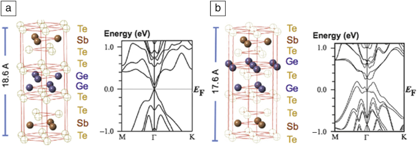
Interestingly, iPCM was originally designed as a nonvolatile resistive switching memory that operates by switching the different bonding states of Ge atoms.Reference Kolobov, Fons, Frenkel, Ankudinov, Tominaga and Uruga15 That is, the bonding state difference appears as a difference in the spatial symmetry.Reference Tominaga, Kolobov, Fons, Wang, Saito, Nakano, Hase, Murakami, Herfort and Takagaki38 These include three different phases—Te-Ge-Ge-Te, Ge-Te-Te-Ge, and Ge-Te-Ge-Te in atomic arrangement along the GeTe[111] direction unit in an iPCM film. The first and second phases satisfy the spatial inversion symmetry, whereas the last phase breaks it, which generates a ferroelectric phase.Reference Kolobov, Kim, Giussani, Fons, Tominaga, Calarco and Gruverman34,Reference Tominaga, Kolobov, Fons, Wang, Saito, Nakano, Hase, Murakami, Herfort and Takagaki38 The symmetry differences are reflected in the electronic band structures, as shown in Figure 3. In the ferroelectric phase, spin degeneracies are lifted, resulting in bands like such as Rashba splits, which are the band states that appear when a high electric field is applied to Au, for example.Reference Sante, Barone, Bertacco and Picozzi39 This phase may be sensitive to an external magnetic field. Ge-Sb-Te alloys do not generally show a magnetic feature at room temperature, although a perfect Ge2Sb2Te5 crystal phase has been predicted to be a TI when a strain is applied.Reference Kim, Kim and Jhi40,Reference Kim and Jhi41 When exchanging Ge and Te atom positions, which is the original switching mechanism in an iPCM device, the first and second phases show remarkably different band structures. It should be noted that the first phase has a Dirac cone at the highest symmetry point even in the bulk state, whereas the second phase has a bandgap. This means that an iPCM film can function in principle for active device switching between a Dirac semimetal and a bandgap insulator (ferroelectric insulator) by controlling the external electric field strength.
Primitive cells of the [(GeTe)2(Sb2Te3)1] superlattice and the band-structure difference. (a) High-resistive phase (called RESET-state) with spatial inversion symmetry and (b) low-resistive ferroelectric phase (called SET-state) with broken symmetry. Note: E F, Fermi energy; M, Γ, and K are k-points in the reciprocal lattice.Reference Tominaga, Kolobov, Fons, Wang, Saito, Nakano, Hase, Murakami, Herfort and Takagaki38

Attempts to induce topological functionalities from iPCM devices
Since the first demonstration of iPCM devices for suppression of the switching energy, the question of whether iPCM devices have topological characteristics has been explored both theoreticallyReference Sa, Zhou, Sun, Tominaga and Ahuja19 and experimentally.Reference Takagaki, Saito and Tominaga42 Approaching a small magnet during a SET and RESET endurance test, we noticed that the SET voltage shifted from 0.8 V to more than 2.0 V, as seen in Figure 4.Reference Tominaga, Kolobov, Fons, Wang, Saito, Nakano, Hase, Murakami, Herfort and Takagaki38 This occurred only when the magnet was close to the device. Such an extraordinary response to an external magnetic field has not been observed or reported in PC-RAM. This magnetic response was observed only when the Ge-Sb-Te alloy film is replaced with a superlattice composed of GeTe and Sb2Te3 sublayers despite both having the same bulk composition ratio. It was also found that the magnetoresistance exceeded more than two orders of magnitude at room temperature.
(a) Magnetoresistance under different magnetic field strengths of 0.8, 1.0, and 1.2 kOe, and (b) the associated resistance hysteresis in a typical interfacial phase-change memory [(GeTe)2/(Sb2Te3)4]8 device (see inset) at room temperature. Magnetoresistance hysteresis occurs after the electric field (E) is turned off with a magnetic field (B) still present. The black circles indicate the initial resistance (R) without an applied magnetic field, the blue circles indicate resistance values with a magnetic field, the red circles indicate the first R–V curve after removal of the magnetic field, and finally the black triangles correspond to the second R–V cycle after the magnetic field was turned off. In each process, the initial and terminated states were both RESET.Reference Tominaga, Kolobov, Fons, Wang, Saito, Nakano, Hase, Murakami, Herfort and Takagaki38 Note: V, voltage.

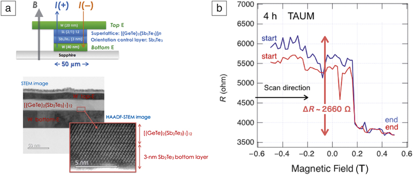
Our group at AIST, Japan, has recently reported detailed magnetic responses and the mechanism of iPCM, using cross-point-type devices.Reference Tominaga, Saito, Mitrofanov, Inoue, Fons, Kolobov, Nakamura and Miyata43 As previously discussed, the iPCM films generally have three different structures in the GeTe sublayers: Te-Ge-Ge-Te, Ge-Te-Te-Ge, and Ge-Te-Ge-Te (ferroelectric) along the GeTe[111] direction, which is normal to the interfaces with Sb2Te3 QLs. As the free energies for the formation of the three structures are almost identical at the iPCM film deposition temperature (∼500 K), the devices usually include a mixture of the three phases.Reference Tominaga, Kolobov, Fons, Wang, Saito, Nakano, Hase, Murakami, Herfort and Takagaki38 In such a mixed state, iPCM devices do not usually show a magnetic response. However, once an iPCM device is exposed to a magnetic field accompanied by electric current pulse injections (repetitive electric field) at high temperature (>470 K) and cooled down to room temperature while holding the fields, the device generates a large magnetoresistance response, as shown in Figure 5. The thermal treatment under an applied magnetic field and electric current injections was named thermal annealing under a magnetic field (TAUM). The lack of one of the fields (either electric or magnetic) cannot generate the magnetoresistance. Moreover, the phenomenon strongly relies on the thickness of GeTe. Since the Ge–Te–Ge–Te (ferroelectric) phase lacks spatial inversion symmetry, spin degeneration in the band structures is lifted, resulting in a response to an external electric field. It is thought that TAUM treatment increases the amount of the Ge-Te-Ge-Te phase in the mixture phase, although intermixing with Sb2Te3 sublayers has been recently discussed.Reference Momand, Wang, Boschker, Verheijin, Calarco and Kooi44–Reference Lotnyk, Hilmi, Ross and Rauschenbach46 The results introduced here are only a portion of the magnetic exciting phenomena that have not been reported yet.
Resistance change at 300 K of [(GeTe)L(Sb2Te3)1]12 (L = 2). (a) (Top) Crosspoint device structure and (bottom) transmission electron microscope image. (b) Resistance (R) responses to external magnetic field after 4 h thermal annealing under a magnetic field (TAUM) treatment with current pulses (I, ±100 μA). Blue and orange lines show the current flow directions from bottom to top, and from top to bottom electrodes (E), respectively. Magnetic field (B) was scanned from –0.5 T to +0.5 T.Reference Kolobov, Kim, Giussani, Fons, Tominaga, Calarco and Gruverman34 Note: STEM, scanning transmission electron microscope; HAADF, high-angle annular dark field; SL, superlattice.

Prospects for topological iPCM devices
The functionalities of spin storage and large magnetoresistance for iPCM devices are promising as future memory devices beyond x-point phase-change memories. Once the present Ge-Sb-Te alloy film is replaced with a superlattice composed of GeTe and Sb2Te3 sublayers, the switching energy can be suppressed to lower than 5 or 10% of present PC-RAM devices. Furthermore, adding two in-plane electrodes in an iPCM device, input and output of spin information could be possible with the help of vertical electric field control. That is, one iPCM unit may work as a spin-flow-circuit equipped with a switching gate. Networking such units using superlattice wires may work as a quantum computer. Such a combination of PC-RAM and MRAM characteristics can yield more functionalized devices, and the advent of such a device should occur in the not-too-distant future.
Acknowledgment
The work was fully supported by Grant No. JPMJCR14F1 of the Japan Science and Technology Agency (JST/CREST).

Junji Tominaga is a prime senior researcher in the Nanoelectronics Research Institute at the National Institute of Advanced Industrial Science and Technology (AIST), Japan. He received his PhD degree from Cranfield University, UK, in 1991. After studying optical phase-change memory at TDK Corporation, he joined AIST in 1997. He was the director of the Center for Applied Near-Field Optics Research until 2009. His research focuses on phase-change materials and application. He is the inventor of super-resolution near-field structure (super-RENS) and the interfacial phase-change memory (iPCM) device. He was awarded the S.R. Ovshinsky Lectureship Award in 2014. He is a Fellow of The Optical Society and a member of IOP. Tominaga can be reached by email at j-tominaga@aist.go.jp.