I. INTRODUCTION
Indium-rich heterostructures with quantum well (QW) InAlAs/InGaAs/InAlAs are among the most attractive materials for the high electron mobility transistors in millimeter wave communications, imaging, and radars.Reference Kim and del Alamo1 The outstanding electron transport properties (the electron mobility µе and saturation velocity v s) in the InGaAs channel enhance considerably with increasing In mole fraction.
Various types of In-rich heterostructures were explored in recent years with a view to achieve the best cutoff frequency. The issue appeared at the increase of InAs content is the plastic relaxation resulting in the crystalline quality deterioration due to the high lattice mismatch between the substrate, InxGa1−xAs channel and InyAl1−yAs barriers. This problem arises for the pseudomorphic technology, which tends to keep stressed InyGa1−yAs layer between the InP substrate and lattice-matched In0.52Al0.48As layer, as well as the metamorphic technology, which prepares an appropriate InxAl1−xAs “virtual substrate” for the necessary QW composition. With the rise of x value the thickness of the coherently stressed InyGa1−yAs goes downReference Drouot, Gendry, Santinelli, Letartre, Tardy, Viktorovitch, Hollinger, Ambri and Pitaval2 and the gradually relaxed metamorphic InxAl1−xAs becomes laterally rough and dislocation-rich.Reference Bollaert, Cordier, Zaknoune, Happy, Hoel, Lepilliet, Théron and Cappy3,Reference Galiev, Vasil’evskii, Klimov, Pushkarev, Klochkov, Maltsev, Presniakov, Trunkin and Vasiliev4 As so, the layer design and epitaxial growth conditions remain the essential problems in the In-rich III–V heterostructure engineering.
One of the existing approaches is that the introduction of a tiny InAs insert layer into lattice-matched In0.53Ga0.47As layer, resulting in the composite quantum well (CQW) with pseudomorphically strained InAs layer.Reference Maeda, Ito, Enoki and Ishii5–Reference Nakayama and Miyamoto7 These InAs inserts modify the band structure and charge spatial distribution in the CQWReference Richter, Koch, Matsuyama, Heyn and Merkt8 and decrease the electron effective mass,Reference Kulbachinskii, Yuzeeva, Galiev, Klimov, Vasil’evskiі, Khabibullin and Ponomarev9 which leads to the electron mobility enhancement.Reference Šilenas, Požela, Požela, Jucienė, Vasil’evskii, Galiev, Pushkarev and Klimov10,Reference Sexl, Böhm, Xu, Heiβ, Kraus, Tränkle and Weiman11 Additionally, such structures can reduce the hot electron scattering by the optical phononsReference Požela, Šilėnas, Požela, Jucienė, Galiev, Vasil’evskii and Klimov12 and serve as a phonon barrier and increase saturation drift velocity.
For the growth of InAs insert, the epitaxial conditions have to be selected accurately due to the high lattice mismatch. The film growth could follow Volmer–Weber or Stranski–Krastanov (3D) mode with the formation of stress-driven nanoislands,Reference Stangl, Holý and Bauer13 which result in the interface roughness (IR), and local fluctuations of the InAs insert thickness. These fluctuations lead to the subband energy level variation and to the electron scattering due to IR. The contribution of IR scattering is negligible for the wide (>10 nm) QWs but becomes dominating in the narrow (<5 nm) QWs.Reference Sakaki, Noda, Hirakawa, Tanaka and Matsusue14 For the CQWs, the thin narrow-band semiconductor layer forms an additional well, which enhance the influence of its thickness variations. Additionally, the strain and InAs insert plastic relaxation have to be controlled. It is known that the critical thickness of the highly mismatched layers depends on composition and growth temperature.Reference Drouot, Gendry, Santinelli, Letartre, Tardy, Viktorovitch, Hollinger, Ambri and Pitaval2 Typical growth conditions of the CQW heterostructures with high electron transport properties require relatively low growth temperature.Reference Sexl, Böhm, Xu, Heiβ, Kraus, Tränkle and Weiman11 The influence of the As4 partial pressure on the formation of the strained InAs films in the thick In0.53Ga0.47As matrix has been reported in Ref. Reference Tournie and Ploog15 where the In-stable conditions were shown to favor the formation of smooth films with high crystalline quality. The goal of the present experiment was to form the dislocation-free InAs inserts with abrupt heterointerfaces inside the In0.52Al0.48As/In0.53Ga0.47As/In0.52Al0.48As QW. We report the measurements of the electrophysical and structural properties of the In0.53Ga0.47As/In0.52Al0.48As nanostructures with thin InAs inserts grown at different As4 pressures.
II. MATERIAL GROWTH AND EXPERIMENTAL PROCEDURE
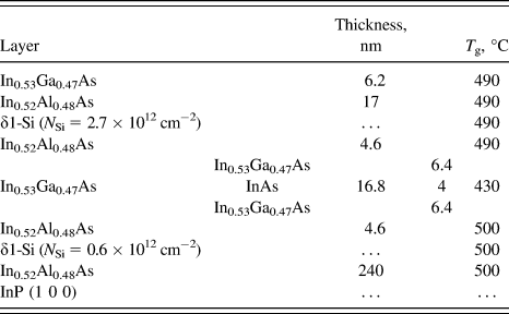
The samples were grown by the solid-source molecular beam epitaxy (MBE) on the semiinsulating Fe-doped epi-ready (1 0 0) InP substrates. The native oxide was removed by the substrate annealing in As ambient with the heating rate 3 °C/min up to 520 °C. After that, temperature was lowered to 500 °C and the growth started immediately. The composition, the width of the heterostructure layers, and growth temperatures are presented in Table I. All investigated samples had identical layer sequence and growth conditions except the QW regions. The active region of the sample 861 was In0.52Al0.48As/In0.53Ga0.47As/In0.52Al0.48As QW with the thickness of 16.8 nm (the basic sample). Samples 865 and 867 had 4 nm InAs inserts in the middle of the In0.53Ga0.47As layer, but the overall thickness of the CQW was the same (16.8 nm). The doping concentrations for bottom and top δ-Si layers were N δ1-Si = 0.6 × 1012 cm−2 and N δ2-Si = 2.7 × 1012 cm−2. An undoped In0.53Ga0.47As cap layer with thickness of 6.2 nm was grown for the protection against an oxidation of InAlAs barrier layer. The growth temperature of the buffer layer was T g = 500 °C, then it was decreased to 430 °C to provide sharper CQW heterointerfaces and to preserve inelastic strain relaxation of the InAs inserts. After the CQW growth T g was increased to 490 °C to complete the structure. On both InGaAs heterointerfaces, the 120 s growth interruptions were performed to reduce IR, combined with the substrate temperature manipulations. The As4 beam equivalent pressure (BEP) in the growth chamber for all runs was P As = 9.8 × 10⁻⁶ Torr. The III group elements BEPs were P Al = 3.0 × 10⁻⁸ Torr, P Ga = 7.3 × 10⁻⁸ Torr, and P In = 1.80 × 10⁻⁷ Torr. The growth rates of the lattice-matched InAlAs and InGaAs layers were around 12 nm/min. The only difference between samples 867 and 865 was reduced As4 BEP to P As = 2.8 × 10⁻⁶ Torr during InAs insert growth for the 865 sample (the V/III BEP ratios during InAs growth were equal to 54 and 16 for 867 and 865 samples, respectively).
The width, composition, and growth temperature of the heterostructure layers.

Electron transport properties of the samples were measured at T = 77 and 300 K in magnetic field of 0.3 T by conventional Hall effect technique on Hall bar mesa structures, formed by electron-beam lithography.
Cross-sectional transmission electron microscopy (TEM) specimens were prepared by mechanical polishing of sandwiched pieces followed by Ar+ ion-beam milling until perforation in Gatan PIPS (Gatan, US). The study was performed in the scanning transmission electron microscope (STEM) TITAN 80-300 TEM/STEM (FEI, Hillsboro, OR) operated at an accelerating voltage of 300 kV, equipped with Cs-probe corrector and high-angle annular dark-field detector (HAADF) (Fischione, US).
III. RESULTS
The measured electron mobility μе and sheet concentration n S for the samples are presented in Table II for T = 77 and 300 K. At both temperatures, the electron mobility and concentration were higher in the samples with InAs inserts, namely 865 and 867, in comparison with basic sample 861 without insert. The highest μе and n S were found in sample 865 which had the lower As4 pressure during InAs growth. The substantial 30% mobility difference at 77 K between 865 and 867 samples indicates that insert growth conditions are essential factor at determining the two-dimensional electron gas transport properties.
Electron transport properties.
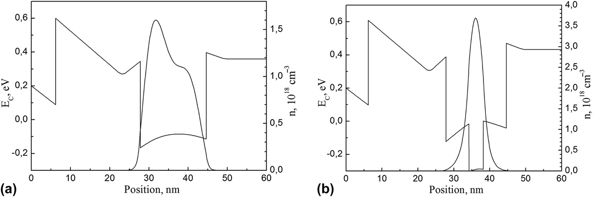
The electron density distribution and conduction band spatial profile were evaluated by solving Poisson–Schrodinger equation system within single-band effective mass approximation.Reference Maeda, Ito, Enoki and Ishii5 The semiconductor compound parameters were taken from Ref. Reference Vurgaftman, Meyer and Ram-Mohan16 The temperature established for simulation was 77 and 300 K. The results are presented in Fig. 1. The presence of the InAs insert affected drastically on electron distribution in the QW. The electron density in the sample without an insert is spreaded over the whole QW layer with electron wave function tails penetrating into the barrier InAlAs regions. The thin insert, which is the narrow-band InAs layer, forms an additional QW and that results in substantial decrease of the electron spatial distribution width. The QW depth increase in the samples with the insert as compared to the uniform InGaAs QW consequences in slightly larger calculated electron density (by 0.1 × 1012 cm−2), as it is shown in Table II. The experimentally observed difference of the electron densities in samples 861, 865, and 867 is much greater.
The calculated conduction band spatial profile and electron density distribution for heterostructures without (a) and with InAs insertion (b).
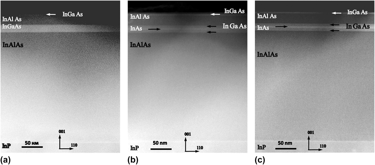
For the evaluation of the InAs insert, crystalline quality conventional and high resolution (HR) TEM/STEM study have been performed. The low magnification HAADF STEM of the basic (861) and samples with the inserts (865 and 867) are presented in Figs. 2(a)–2(c), respectively. Due to pronounced Z-contrast, defect-free InAlAs buffer layer, QWs and InAs inserts in 865 and 867 samples are clearly visible. At the substrate/buffer layer interface, a bright band having thickness of ∼1 nm was found. This layer could be formed during the removal of the oxide layer on the substrate surface in the As4 flux when the surface P atoms were substituted by As.Reference Watanabe, Isu, Hata and Katayama17 Some contrast variation in the images appeared due to different thicknesses of the specimens.
The HAADF STEM images of the samples: (а) sample 861, (b) 867, and (c) 865.
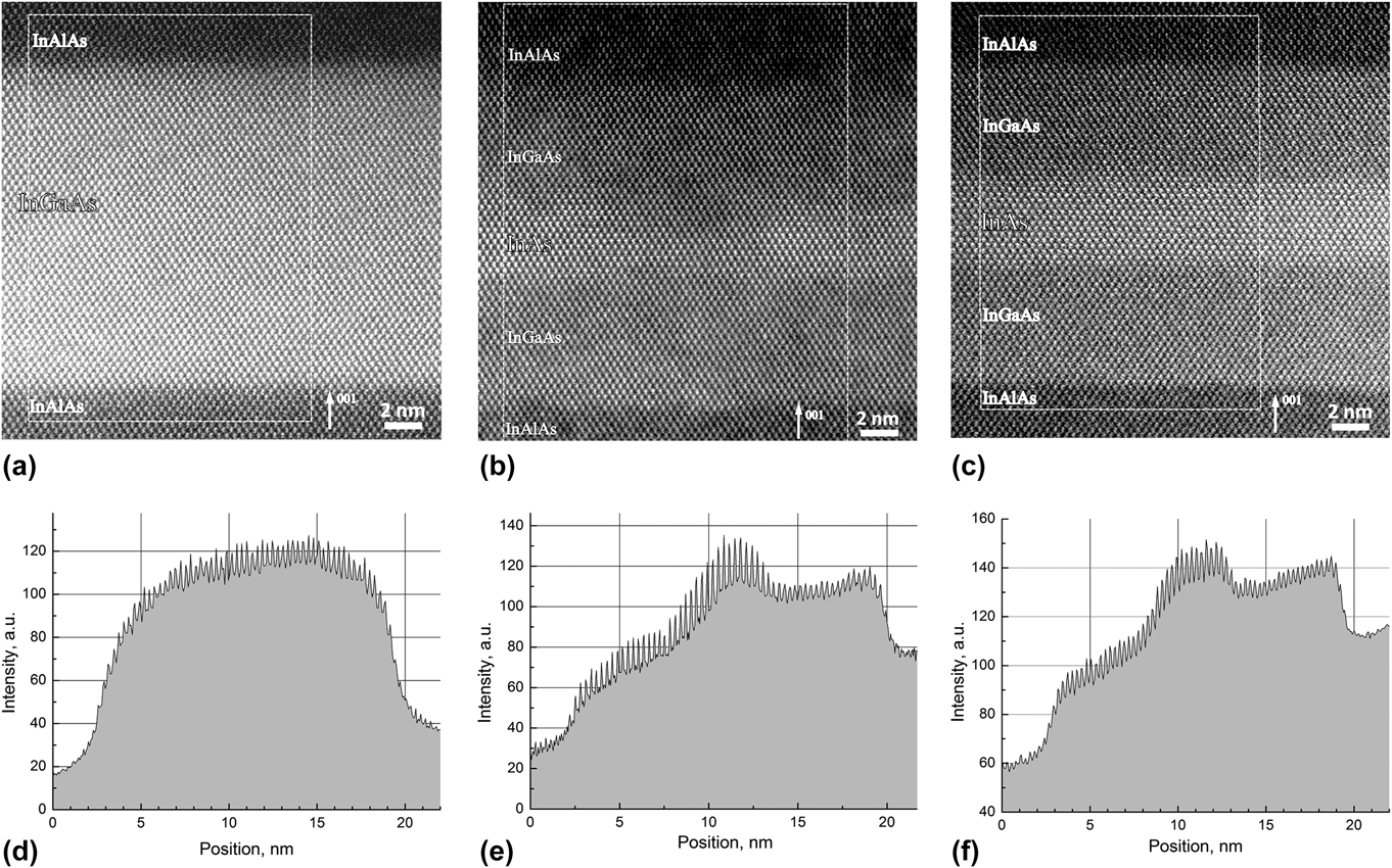
HR HAADF STEM images of the QW areas are presented in Figs. 3(a)–3(c) for the samples 861, 867, and 865, respectively. The areas with the brightest contrast correspond to the layers with high In content. The intensity profiles averaged over the rectangular areas denoted by thin dashed lines in Figs. 3(a)–3(c) are shown in Figs. 3(d)–3(f). The origin of the diagrams corresponds to the top of the QW images. All InAlAs/InGaAs and InGaAs/InAs interfaces are sharp, the roughness, estimated roughly from these images, does not exceed few unit cells dimensions.
HR HAADF STEM images of the QW areas of sample: (a) 861, (b) 867, and (c) 865. Correspondent intensity profiles of the images averaged over the rectangular areas denoted by thin dashed lines (from the top to the bottom of the QWs) for sample: (d) 861, (e) 867, and (f) 865.
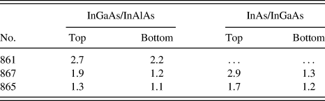
The heterointerfaces contain transitional monolayers with elements intermixing. The width of the heterointerfaces, namely top and bottom In0.53Ga0.47As/In0.52Al0.48As interface, and top/bottom InAs/In0.53Ga0.47As interface, were estimated by the evaluation of the STEM intensity profiles shown in Figs. 3(d)–3(f) and these data are presented in Table III. The corresponding values depend on the atom intermixing during MBE. The larger width and consequently broader interfaces were found for the top interfaces of the QWs or InAs inserts. Such effect can be explained by high In segregation coefficient and technological asymmetry of the growth sequence. Before the QW growth, the temperature T g was decreased from 500 to 430 °C and after the QW formation it was increased to 490 °C, enhancing the atom diffusion at the upper heterointerface to the lower one.
QW interface widths, nm.
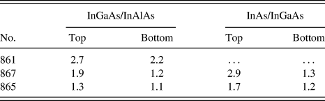
The comparison of the Figs. 3(b) and 3(c) demonstrated that the roughness of InAs/InGaAs insert interfaces is smaller in the sample 865 than in the sample 867. The top InAs/InGaAs interface in the sample 867 is blurred and that is clearly visible on the intensity diagrams Figs. 3(e) and 3(f). In addition, the contrast variations, especially in the upper InGaAs layer of sample 867 [Fig. 3(c)], are visible and these could appear due to the lateral composition fluctuations. These contrast variations correlate with the insert IR. The contrast variations in the same area of the sample 865 are much lighter which pointed to higher homogeneity of the CQW.
IV. DISCUSSION
The increase of electron mobility in the CQW samples 865 and 867 can be explained as follows. As can be seen in Fig. 1, the intercalation of InAs in the QW results in substantial electron localization in the insert region and in the vanishing of the electron wave function tales in the InAlAs barriers. Consequently, the electron effective mass should diminish and remote impurity and alloy disorder scattering mechanisms should decrease. Simulations have shown that the weighted average effective electron mass  $m_{{\rm{weight}}}^*$ in the first subband of the QW
 $${1 \over {m_{{\rm{weight}}}^*}} = \int_{ - \infty }^\infty {{{\left| {\psi \left( z \right)} \right|}^2}} {1 \over {{m^*}\left( z \right)}}{\rm{d}}z\quad ,$$
decreases from 0.044m 0 to 0.030m 0 due to InAs insert, where m 0 is a free electron mass, ψ(z)—electron wave function of the first subband, m(z)—position dependent effective mass. It means that electron mobility should rise in 1.47 times after InAs insert forming if all the electron scattering mechanism rates remained the same. We suppose that electron mobility in the CQWs with thin InAs inserts is determined by the structural quality of the inserts and its heterointerfaces. If so, mobility increase in CQW can be masked by the rise of such structure imperfection scattering mechanisms as IR or compositional nonuniformity scattering.
The TEM measurements indicate that CQW is much more uniform for the 865 sample with flat heterointerfaces. The only difference between 865 and 867 samples was the As4 flux pressure changes during MBE. The influence of such MBE parameter as growth temperature on the InAs insert crystalline quality is reported in Ref. Reference Sexl, Böhm, Xu, Heiβ, Kraus, Tränkle and Weiman11. Temperature reduction from 470 to 420 °C was shown to suppress strain relaxation and defect generation in InAs insert. In our work, other MBE parameter—As4 pressure—is changed during InAs insert growth. The effect of the As4 pressure reduction on the InAs film crystalline quality in the thick In0.53Ga0.47As matrix was reported in Ref. Reference Tournie and Ploog15. It was shown that In-stable growth conditions with BEP <1 inhibit the InAs islands formation and inelastic strain relaxation. In contrast to these results, our samples were grown under As-stable growth conditions. High P As during formation of strained InAs layer for the 867 sample could limit the surface migration rate of In atoms and resulted in the lateral inhomogeneity of insert composition and substantial IR.
V. CONCLUSIONS
The increased electron mobility and concentration was found in the heterostructures with composite InGaAs QWs containing 4 nm thick InAs layer in the middle of the QW as compared with the uniform QW. This effect was explained by the QW depth increase and the improvement of electron localization in the InAs insert. It was revealed that the As4 flux during the InAs insert growth influenced structural quality of the InAs layer, notably interface widths and lateral composition homogeneity. The decrease of the V/III BEP ratio from 54 to 16 resulted in substantial improving of the InAs layer structural quality and CQW mobility and concentration enhancement.
ACKNOWLEDGMENT
This work is supported by the Ministry of Education and Science of the Russian Federation (research identifier RFMEFI60414X0003).