I. INTRODUCTION
Vanadium dioxide (VO2) single crystals exhibit an extremely abrupt first-order phase transformation from a semiconducting monoclinic phase, with a P21/C space group, to a metallic tetragonal phase, with a P42/mnm space group, at about 68 °C.Reference Eyert1–Reference Gupta, Aggarwal, Gupta, Dutta, Narayan and Narayan5 This semiconductor to metal transition (SMT) affects the optical and electrical properties making VO2 an attractive material for a variety of technological applications such as sensors,Reference Ko and Ramanathan6 smart windows,Reference Kato, Song, Odaka and Shigesato7 optical switching,Reference Becker, Buckman, Walser, Lepine, Georges and Brun8 energy management devices,Reference Soltani, Chaker, Haddad and Kruzelesky9 actuators,Reference Rajendra Kumar, Karunagaran, Mangalaraj, Narayandass, Manoravi, Joseph and Gopal10 and photochromic memories.Reference Chivian, Scott, Case and Krasutsky11 The SMT in VO2 involves a small lattice distortion along the c-axis, which results in failure of VO2 bulk single crystals when subjected to repeated heating and cooling cycles.Reference Gupta, Aggarwal, Gupta, Dutta, Narayan and Narayan5, Reference Goodenough12, Reference Lazarovits, Kim, Haule and Kotliar13 Therefore, VO2 thin films and nanoparticles, which are able to sustain these distortions and dissipate heat through the substrate, are needed for a variety of technological applications. So far, most of the studies on VO2 thin films have been focused on growth of epitaxial films with controlled properties on Al2O3 and TiO2 substratesReference Okimura, Sakai and Ramanathan14, Reference Muraoka, Ueda and Hiroi15; however, implementation of VO2-based devices is restricted by the limited use of Al2O3 and TiO2 substrates in the microelectronic industry. An essential prerequisite to the development of optoelectronic devices based on thermal switching is the integration of VO2 films with Si(001), which is the mainstay substrate material in the microelectronics industry. This epitaxy on Si(100) also allows integration of functionality on a computer chip for smart device functions.Reference Fang, Adomi, Iyer, Morkoç, Zabel, Choi and Otsuka16 Though the epitaxial growth of VO2 on Si(001) can be anticipated via domain matching epitaxy (DME),Reference Narayan and Larson17 where integral multiples of planes match across the film–substrate interface, direct deposition of epitaxial VO2 on Si(001) remains a technological challenge due to the formation of silicides or native amorphous silicon dioxide layers. In this research, we have addressed the integration of high quality epitaxial VO2/NiO thin film heterostructures with Si(001) substrates by cubic yttria-stabilized zirconia (YSZ) buffer system. Introduction of NiO platform provides a complete relaxation of misfit strain, which leads to a negligible tension/compression along the VO2[001] direction. The tensile strain in VO2[001] increases the SMT temperature, while the compressive strain decreases the SMT temperature, compared to the bulk value. Thus, we can combine the positive characteristics of VO2and NiO and develop a new system with novel properties suitable for integrated and reliable device applications.
Nickel oxide (NiO) is a p-type semiconducting material with a band gap of 3.6–4.0 eV and has been introduced as a promising candidate for a wide range of applications such as solar cells,Reference Bandara and Weerasinghe18 spin-valve giant magnetoresistance sensor,Reference Hwang, Lee and Park19 transparent conducting electrodes,Reference Chan, Hsu and Hong20 gas sensors,Reference Hotovy, Huran, Siciliano, Capone, Spiess and Rehacek21 electrochemical display devices,Reference Granqvist, Avendano and Azens22 and organic light emitting diodes.Reference Wei, Yamamoto, Ichikawa, Li, Fukuda and Taniguchi23 Moreover, NiO has been used in the fabrication of oxide p–n junctions as the p-type layer.Reference Yang, Shi, Feng, Pu, Li, Zhou and Zhang24 Potential applications of NiO as an epitaxial electrode or gate oxide layer can open up exciting possibilities in devices based on SMT properties of VO2thin films.Reference Gupta, Narayan and Dutta25, Reference Gupta, Singhal, Narayan and Avasthi26
Epitaxial growth of VO2/NiO on Si(001) represents a major milestone toward achieving VO2-based smart sensor or memory-based devices. Fully relaxed VO2/NiO thin film heterostructures hold a significant technological importance since the SMT characteristics can be influenced by the misfit strains. In this study, special emphasis is placed on the growth of high quality single crystalline thin film heterostructures and explaining the epitaxial relationships across the interfaces in accordance with the DME paradigmReference Narayan and Larson17 where integral multiples of planes match across the film–substrate interface. We could achieve a near bulk and sharp SMT in the VO2/NiO/YSZ heteroepitaxy through engineering the interfaces and relaxing the strains.
II. EXPERIMENTAL
The VO2/NiO/YSZ heterostructures were grown on Si(100) substrates by the pulsed laser deposition (PLD) technique. PLD is a versatile technique to deposit high quality thin films by optimizing the laser and substrate variables.Reference Narayan and Bhosle27–Reference Koch, Johnson, Kumar, Jelinek, Chrisey, Doraiswamy, Jin, Narayan and Mihailescu29 The silicon substrates were cleaned by boiling in acetone at 200 °C for 5 min, followed by ultrasonic cleaning in acetone (5 min) and methanol (5 min) at room temperature. The substrates were fully dried by purified nitrogen and loaded to the deposition chamber immediately. The chamber was evacuated to a background pressure of about 1 × 10⁻⁶ Torr. During the deposition, oxygen partial pressure was controlled by leaking oxygen into the chamber. A Lambda Physik (LPX200) KrF excimer laser (Lambda Physik AG, Goettingen, Germany) with a wave length of 248 nm and pulse duration of 25 ns was used to ablate the high purity targets being rotated during the deposition to avoid pitting on the target. To fully eliminate the native SiO2 amorphous layer, the YSZ buffer layer was deposited under vacuum for 500 pulses and under an oxygen atmosphere at a pressure of 5 × 10⁻⁴ Torr for 1500 pulses at 700 °C.Reference Aggarwal, Jin, Pant, Narayan and Narayan30 Without breaking the vacuum, the NiO films were grown at 700 °C under the pressure of 5 × 10⁻⁴ Torr for 4500 pulses. Finally, the VO2 films were deposited at 500 °C under the oxygen pressure of 1 × 10⁻² Torr for 4500 pulses. Repetition rate, laser energy density, and the target–substrate distance were the same for all films and maintained at 5 Hz, 3–3.5 J/cm2, and 4.5 cm, respectively. The films were cooled down to the room temperature inside the PLD chamber under the growth pressure.
The phase structure and the out-of-plane orientation of the films were studied by θ/2θ scan x-ray diffraction (XRD) using a Rigaku x-ray diffractometer (Rigaku, The Woodlands, TX) with a Cu Kαradiation at λ = 1.54 Å. Using a Panalytical X'Pert PRO MRD HR X-Ray diffractometer (ϕ-scan) (PANalytical, Almelo, Netherlands), the in-plane alignment of the films was determined as well. A JEOL-2010F field emission transmission electron microscopy (TEM) (JEOL Ltd., Tokyo, Japan) was used to study the atomic and crystallographic arrangements across the interfaces and to confirm the epitaxial growth of the films. A self-made labview program using a Keithley 2400 sourcemeter (2400 Keithley Instruments Inc., Cleveland, OH) was used to study the electrical properties and the SMT behavior of the heterostructures. The measurements were done in a temperature range of 325–355 K where the sample was cooled using a closed cycle helium cryostat.
III. RESULTS AND DISCUSSION
A. Out-of-plane orientation
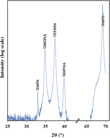
The θ/2θ XRD pattern of the VO2/NiO/YSZ/Si(001) heterostructure is depicted in Fig. 1. The pattern shows that VO2 only grows along its b-axis or c-axis and other orientations are absent. The VO2 peak at 39.8°, which has shifted by ∼0.1° from the Bragg’s angle of VO2(020) reflection, may be attributed to either (002) or (020) orientations since the interplanar spacing of low temperature monoclinic phase of VO2 along the [010] and [001] orientations are to some extent similar (d 020 = ∼d 002 = ∼2.26 Å, a = 5.743, b = 4.517, and c = 5.375 Å).Reference Longo and Kierkegaard2 To distinguish the growth orientation of the VO2 film, ϕ-scan measurement was conducted on the  ${\rm{VO}}_{\rm{2}} (\bar 102)$ reflection (2θ = 33.39°). This reflection has angular separations of 27.8° from (002) and 90° from (020) planes. No ϕ-peak was observed when the ψ-angle was set at 27.8° (data not shown here) indicating that the XRD peak at 39.8° corresponds to VO2(020) and not to VO2(002). Meanwhile, the absence of any other peaks of vanadium oxide indicates that other phases of vanadium oxide have not been formed. The θ/2θ pattern also shows that the YSZ buffer layers and the NiO films grow along [001] and [111] orientations, respectively.
θ/2θ XRD pattern of the VO2/NiO/YSZ/Si(001) thin film heterostructure.

B. In-plane orientation
1. YSZ/Si(001) interface
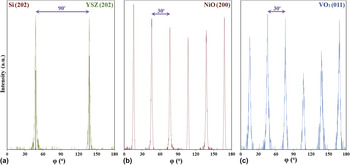
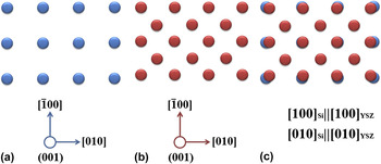
To study the epitaxial relationship between the YSZ buffer layer and the silicon substrate, ϕ-scanning XRD was performed on the YSZ(202) reflection at 2θ = 50.37° and ψ = 45.00° and on the Si(202) reflection at 2θ = 47.57° and ψ = 45.00° [Fig. 2(a)]. As is seen, the ϕ-peaks from (202) reflections of YSZ and Si appear at the same azimuthal positions due to the 4-fold symmetry in both crystals and their approximately similar lattice parameters (a Si = 5.43 and a YSZ = 5.14 Å). The epitaxial relationship between the YSZ film and the Si(001) substrate was explained as a cube-on-cube growth: {001}YSZ‖{001}Si and <100>YSZ‖<100>Si. The atomic arrangement across the YSZ/Si interface was modeled, as shown in Fig. 3. The misfit strain across the YSZ/Si interface was calculated as ∼5.3%, which is relaxed by alternating of 18/17 and 19/18 domains with a frequency factor of about 0.7, according to the DME paradigm.Reference Narayan and Larson17
ϕ-scan XRD pattern acquired from: (a) YSZ(202) and Si(202), (b) NiO(200), and (c) VO2(011) reflections.

Atomic arrangement at the: (a) Si(001) surface, (b) YSZ(001) surface, and (c) YSZ/Si interface.

2. NiO/YSZ interface
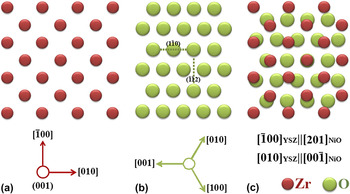
The ϕ-scan XRD was conducted on the (200) reflection of NiO (2θ = 43.31° and ψ = 54.24°) to investigate the epitaxial relationship at the YSZ/NiO interface and the results are depicted in Fig. 2(b). The appearance of six sharp peaks confirms the epitaxial growth of NiO on the YSZ buffer layer. The presence of these strong peaks with a 30° angular separation is attributed to the 3-fold symmetry of the NiO structure along the [111] direction and four crystallographically equivalent directions on the cubic YSZ structure, which has a 4-fold symmetry. Considering these results, the epitaxial relationship between the YSZ and NiO films was expressed to be (001)YSZ‖(111)NiO and  $[010]_{{\rm{YSZ}}} \parallel [00\bar 1]_{{\rm{NiO}}}$. The atomic arrangement at the YSZ/NiO interface is modeled and the corresponding results are presented in Fig. 4. Because both YSZ buffer layer and NiO films were deposited under the pressure of 5 × 10⁻⁴ Torr, surface of the YSZ layer would be Zr terminated [Fig. 4(a)]. As a consequence, an O-terminated surface of NiO film grows onto the cation-terminated buffer layer. The O-terminated surface of NiO is schematically illustrated in Fig. 4(b). The misfit strain at the interface along the a-axis of the YSZ buffer layer was determined as
 ${\rm{\varepsilon }}_1 = 1 - (d_{(1\overline 1 0){\rm{NiO}}} /d_{(100){\rm{YSZ}}} ) \,= \,42.6\% $, which is fully relaxed through alternating of 3/2 and 2/1 domains with a frequency factor of about 0.34. The misfit strain along the b-axis of the YSZ layer was calculated as
 ${\rm{\varepsilon }}_2 = 1 - (d_{(\overline 1 \overline 1 2){\rm{NiO}}} /d_{(020){\rm{YSZ}}} ) = 33.5\% $, which is accommodated by matching of two planes of NiO with one plane of YSZ or three planes of NiO with two planes of YSZ where the frequency factor is about 0.99. That is, a kind of a perfect 3/2 matching takes place at the YSZ/NiO interface along the [010] direction of YSZ. Figure 4(c) shows the atomic arrangement at the YSZ/NiO interface.
Atomic arrangement at the: (a) Zr-terminated YSZ(001) surface, (b) O-terminated NiO(111) surface, and (c) NiO/YSZ interface.

3. VO2/NiO interface
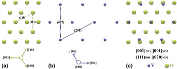
The in-plane alignment of the VO2 film was studied by doing ϕ-scan XRD on the (011) reflection of VO2 (2θ = 27.80° and ψ = 45.00°). In this case, six peaks with an azimuthal separation of 30°, aligned with the (200) reflection of NiO, were observed [Fig. 2(c)]. The reasons why six ϕ-peaks were observed are that the VO2 film has a 2-fold symmetry along its b-direction and there are three equally probable variants of VO2, rotated by 120° from each other, on the NiO(111) platform. Moreover, we already showed that there are four equivalent variants in the NiO film. Based on this information, the epitaxial relationship between the VO2 and NiO films was (010)VO2‖(111)NiO and [001]VO2‖[110]NiO. The misfit strains across the NiO/VO2 interface were determined to be  ${\rm{\varepsilon }}_1 = 1 - (d_{(\overline 4 07){\rm{VO2}}} /d_{(\overline 2 \overline 2 4){\rm{NiO}}} ) = 33.2$ and
 ${\rm{\varepsilon }}_2 = 1 - (d_{(20\overline 1 ){\rm{VO2}}} /d_{(2\overline 1 \overline 1 ){\rm{NiO}}} ) = - 24.9\% $. These planes are shown in Fig. 5 by dashed lines. The misfit strain along direction 1 (ε1) is fully relaxed through a perfect 3/2 matching (frequency factor is near 0). To fully relax the misfit strain along direction 2 (ε2), 4/5 and 5/6 domains alternate where the frequency factor is about 0.01. Because the oxygen partial pressure was increased from 5 × 10⁻⁴ Torr (oxygen pressure for NiO deposition) to 1 × 10⁻² Torr (oxygen pressure for VO2 deposition), surface of the NiO inner layer gets O terminated, which is illustrated in Fig. 5(a). Hence, a cation (vanadium)-terminated surface of VO2 [Fig. 5(b)] grows onto the NiO film. The atomic arrangement between the NiO and the VO2 thin films is depicted in Fig. 5(c).
Atomic arrangement at the: (a) O-terminated NiO(111) surface, (b) V-terminated VO2(010) surface, and (c) VO2/NiO interface.

Microstructural studies were completed by TEM imaging and diffraction. Figure 6 displays the bright field cross-sectional image of the VO2/NiO/YSZ/Si(001) heterostructure. The epitaxial growth and the proposed epitaxial relationships are confirmed by the indexed selected area pattern, shown in the inset of Fig. 6. The columnar structure in the NiO film indicates the in-plane rotation of the grains, as discussed earlier. Such a structure is not observed in the YSZ buffer layer because of the cube-on-cube epitaxial growth. The selected area electron diffraction (SAED) pattern (inset of Fig. 6) shows the diffraction spots from Si[110] and YSZ[110] and  ${\rm{NiO[}}1\bar 10]$ zones. Due to different in-plane orientations of VO2, the diffraction spots from two zones of VO2, namely [207] and [301], were also observed simultaneously. These results are consistent with details of the epitaxial relationship between Si, YSZ, NiO, and VO2 that were obtained from XRD studies. According to the TEM cross-sectional image, the thickness of the YSZ, NiO, and VO2films were determined as about 49, 63, and 50 nm, respectively.
TEM cross-sectional bright field image of the VO2/NiO/YSZ/Si(001) heterostructure and the SAED pattern (Si[110], YSZ[110],  ${\rm{NiO[}}1\bar 10]$, VO2[201], and VO2[307] zones).

During the initial stages of the deposition where the YSZ buffer layer is deposited under vacuum, the SiO2 amorphous layer is destroyed and removed by the following reactionReference Wang, Ong, You and Xu31:
 $${\rm{Zr}} + {\rm{2SiO}}_{\rm{2}} \to {\rm{ZrO}}_{\rm{2}} + {\rm{2SiO}}\quad{\rm{.}}$$
Then, the YSZ buffer layer grows epitaxially on silicon. The very thin SiO2layer, which is observed in the TEM cross-sectional images, forms during the growth of the films when oxygen diffuses toward the silicon surface through the YSZ buffer layer. However, this phenomenon does not alter the epitaxial growth of the buffer layer because the buffer layer has been already formed.Reference Bayati, Gupta, Molaei, Narayan and Narayan32
C. Semiconductor to metal transition
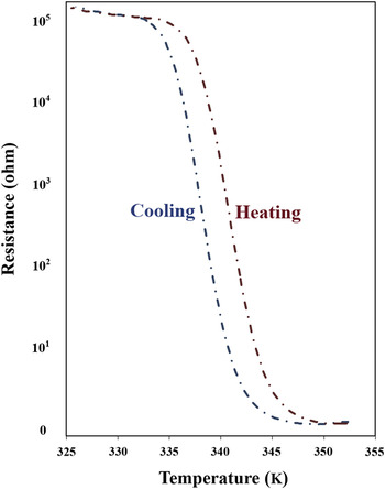
Figure 7 shows the electrical resistivity of the VO2/NiO/YSZ/Si(001) heterostructure as a function of the temperature where a SMT is observed at about 341 K, which is close to the transition temperatures reported for the bulk VO2. The SMT characteristics are excellent in terms of amplitude of the resistivity change (>104 Ωcm) and the sharpness of the transition region (∼3.4 K hysteresis). Such a shift of transition temperature toward that of the bulk VO2 is attributed to strain relaxation along c-axis of VO2. This was achieved by complete relaxation of misfit strain across the VO2/NiO interface resulting in a negligible tension or compression along the c-axis of VO2. The small width of the transition hysteresis reveals growth of the high quality VO2films with negligible defect content.
Resistivity as a function of the temperature for the VO2/NiO/YSZ heterostructure.

Complete strain relaxation in epitaxial VO2 thin films deposited on epitaxial NiO buffer layer was discussed in Sec. III. B. 3. Because the strain along the c-axis of VO2 affects the SMT temperature,Reference Koo, Yoon, Kwon, Ko, Shin, Bae, Chang and Park33 complete relaxation of strain along the [001] direction of VO2 films deposited on epitaxial NiO buffer causes SMT to occur at ∼341 K. As it was explained back in Sec. III. B. 3, the lattice misfits across the VO2/NiO interface were 33.2% and 24.9% along two different crystallographic directions, which were accommodated by a kind of perfect 3/2, 4/5, and 5/6 matchings. According to the DME model, the film grows until a “critical thickness” is reached where the strain energy becomes large enough to trigger the nucleation of misfit dislocations. These dislocations nucleate at the film surface and glide to the interface to relieve the misfit strains.Reference Bayati, Molaei, Narayan, Narayan, Zhou and Pennycook34 In such large misfit systems, the critical thickness is less than one to two monolayers, so the misfit dislocations are generated at or within a monolayer of the interface. Therefore, they nucleate on the VO2-free surface at the very beginning of the growth and glide toward the VO2/NiO interface easily due to the small glide distance. Hence, the misfit strain is relaxed and the remainder of the VO2film grows virtually strain without any misfit dislocation resulting in the observed superior SMT characteristics.
IV. CONCLUSION
The VO2/NiO/YSZ epitaxial thin film heterostructures were grown on Si(001) substrates. The epitaxial relationship at the YSZ/Si(001) interface was determined as (001)[100]YSZ‖(001)[100]Si. The epitaxial relationship between the YSZ buffer layer and the NiO thin film was written as  $(001)[010]_{{\rm{YSZ}}} \parallel (111)[00\overline 1 ]_{{\rm{NiO}}} $. The epitaxial relationship across the NiO/VO2 interface was expressed as
 $(010)[001]_{{\rm{VO2}}} \parallel (111)[00\overline 1 ]_{{\rm{NiO}}} $. All the proposed epitaxial relationships were confirmed by TEM diffraction pattern. A sharp and near bulk SMT was observed at about 341 K with amplitude over four order of magnitude and 3.4 K hysteresis. This is consistent with near complete relaxation of stress in thin films. Such epitaxial structure integrated with Si(100) can be used to enhance functionality and obtain smart devices that are quite reliable due to the absence of initial strains/stresses.
ACKNOWLEDGMENT
We appreciate the financial supports by the National Science Foundation (Grant No. DMR-0803663).