I. INTRODUCTION
The stop-band upper limit of distributed filters, including microstrip band-pass filters, is determined by harmonic or other spurious responses. A previous work on wide pass-band filters [Reference Huang1], which employed quarter-wave resonators where even-order resonances are already absent, combined four methods to suppress the odd-order harmonics to produce a wide stop band with high rejection.
First, resonators with additional stubs, which had the same fundamental but different higher order resonances, that is, stagger-tuned resonators were employed. Previously [Reference Lin, Deng, Lin, Wang and Chen2–Reference Hong and Chang9], stubs or stagger tuning were not used in combinations of several techniques. In [Reference Huang10], the stagger tuning was effected by additional open-ended stubs. The type of main resonators can be chosen independently from the stubs, for compactness, or low loss, or insensitivity to over-etch, a feature retained in [Reference Huang1] and in the current work. In the second suppression technique, the overlap between two parallel-coupled resonators was adjusted for minimal coupling at the spurious frequencies, as previously done in [Reference Kuo, Chen and Jiang11–Reference Huang and Cheng16]. Thirdly, as in [Reference Lee, Cho and Yun17–Reference Tu19], wherever two quarter-wavelength resonators were coupled with a capacitive pad or stub, higher order responses were suppressed or the stop band improved generally, since the pad is like a short circuit at higher frequencies. Finally, resistive attenuation that is significant only in specific resonator modes [Reference Huang20–Reference Huang22] was adopted in one filter. A contrasting work on harmonic suppression is [Reference Akra, Pistono, Issa, Jrad and Ferrari23]: narrow band filters are designed and shorted stubs are used, showing the wide range of this field.
In the present work, the rectangular capacitive coupling pads in [Reference Huang1] are replaced by step-impedance pads, providing up to an estimated 12 dB of further attenuation in the upper part of the broad stop band where there are more resonances, a substantial improvement in its own right. They also provide for a more compact filter. The previous nearly symmetrical layouts were sacrificed. Furthermore, the existing stagger tuning is used to much greater effect, extending suppression to the ninth order; in [Reference Huang1], it was underutilized as it provided mainly reduced sensitivity to fabrication and simulation errors, together with only 2 dB improvement in suppression. Finally, replacing uniform lines with step-impedance resonators (SIRs), the higher order resonances are shifted upwards [Reference Makimoto and Yamashita5, Reference Fathelbab and Steer24], which widens the stop band.
Instead of designing new filters, the two sixth-order, quarter-wave microstrip 42% bandwidth filters centered at 1 GHz described in [Reference Huang1] were upgraded, fabricated, and measured; this was necessary to allow direct comparisons. The design process depends heavily on iterative simulations because of the microstrip dispersion at the high-end of the stop band, the large number of step discontinuities, the near-neighbor spurious interactions, and the wide bandwidth preclude useful simplifying approximations. However, the initial design involved simulating smaller groups of pads and resonators instead of the whole filter, which is one or two orders of magnitude faster; together with a qualitative knowledge of stub behavior and faster computers, it is a viable design procedure.
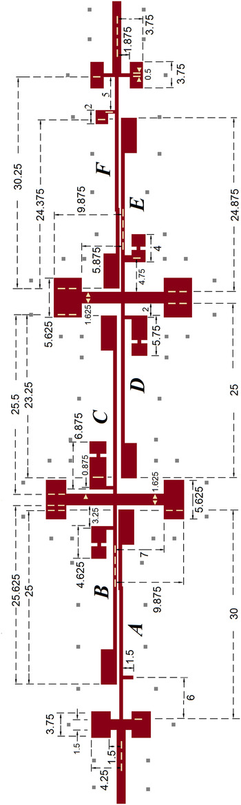
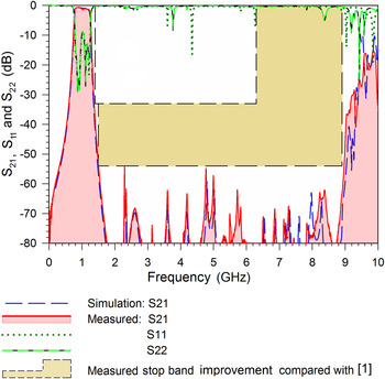
Both filters have the form given in Fig. 1. Coupling from input to resonator A, from B to C, from D to E, and from F to output are via capacitive step-impedance pads, while there is parallel coupling from A to B, C to D, and E to F. In filter 1, with no resistors, stop-band attenuation was improved from 33 [Reference Huang1] to 54 dB, while the stop-band width (previously 1.4–6.3 GHz) was improved (to 1.5–8.9 GHz); this is a width increase of 1.5 times. For filter 2, with resistors, the improvement in attenuation was from 50 to 67 dB, and the stop-band width was 1.8 times wider. According to one figure of merit to be discussed, the filters are 2.4 times better than [Reference Huang1].
Layout of filter 1. In filter 2, the waists in stubs B to E are removed, with the gaps to be bridged by chip resistors. Dimensions in mm. Gray squares show positions of vias forming the side walls.

II. RESONATING STEP-IMPEDANCE COUPLING PADS
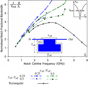
The coupling pads (Fig. 1) are labeled A, BC, DE, and F according to the resonators to which they are connected. They have the shape of a T and an inverted T with their bases connected to the resonators. In the pass band, they act approximately as capacitances. A single, inverted T-shaped pad is inset in Fig. 2.
Normalized notch fractional bandwidth obtainable with rectangular and step-impedance pads.

In a simulation, the substrate thickness h is 0.3 mm, and there is an overlay of h 2 = 1 mm [Reference Huang1] so that the medium is virtually homogeneous, to avoid a complication of variable effective permittivity. Dielectric constant is 10.2, and losses are ignored. For comparisons, the effective pad areas should be equal for approximately equal pass-band coupling, in this case 50 mm2. Due to the fringing electric fields, the effective dimensions are larger than the physical sizes, accounted for by adding an additional border of width h around the pad [Reference Huang1].
SONNET® simulations for step-impedance pads are compared with rectangular pads [Reference Huang1] in Fig. 2. Notch center frequency is varied by varying the pad dimensions. Y eff differs significantly from a quarter wavelength as explained in [Reference Huang1] for the rectangular pads and because of the step impedances here. For each center frequency, X eff and Y eff are not equal among the different pads, but extreme sizes are X eff = 2 mm, Y eff = 33 mm on the left-hand side of the graph, and X eff = 16 mm, Y eff = 5 mm on the right. The normalized notch fractional bandwidth is (1/S 21B ) (B/f 0) as defined in the inset. For h = 0.3 mm, this differs from the normalization in [Reference Huang1] by (coincidentally) a factor of 10.0.
Step-impedance pads can create a wider notch, up to 1.5 times that of the rectangular pad to suppress spurious resonances. Equivalently, they can be said to be 3.5 dB deeper over quite a large frequency band, as discussed in Section 4, where the cumulative effect of more than one pad at any single frequency can be large. The frequency at which the maximum notch width occurs can be adjusted by varying x eff ; for example, for y eff /Y eff = 0.25, increasing x eff from 0.25X eff to 0.5X eff (changing from the blue to the green curve). Small values of y eff are preferable, but may have to be compromised by other design considerations. The notch width increases rapidly toward the right-hand side of the graph, but this is not useful because the depth of the notch suddenly decreases and the pad is then sensitive to fabrication errors.
At the higher order resonances, the step-impedance pads resemble radial stubs [Reference Atwater25, Reference Giannini, Sorrentino and Vrba26], but with step changes in width. Using a larger y eff and forfeiting some of the available suppression gives a narrow waist, which allows neighboring resonators to overlap with the pads, making a more compact filter. They are shorter (in the Y direction) than the uniform rectangles, which also reduces filter size.
III. STAGGER TUNING USING STUBS
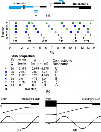
An isolated resonator, resonator C, for example (Fig. 3(a)), is analyzed using transmission line theory, similar to [Reference Huang1, Reference Huang10, Reference Mondal and Mandal27, Reference Huang28], with the resistor and capacitor removed (shorted), and without resonator B. By selecting stub lengths and characteristic impedance, together with the tapping point, in trial and error calculations, the frequencies of the higher order resonances are chosen. For one particular set of stubs, the resonances are shown in Fig. 3(b). The resonance order is given for the resonator with no stub, but for the others, the standing wave pattern is modified so it is not always easy to define the resonance order. The effect on the first-order resonances at f 0 is minimal, as required. The third-order resonances near 3f 0 are still close together, but they will be attenuated by the other techniques. The higher order resonances are well spaced except in a few cases especially near f/f 0 = 11, which will be dealt with by the step-impedance pads and with subsequent iterative adjustments.
(a) Transmission line approximation (resistor, capacitor, and transmission lines) of resonators B and C. (b) Resonance frequencies of one set of stagger-tuned resonators estimated analytically. Resonance order of the stub-free resonator is indicated. (c) Voltage standing wave patterns at fundamental and fifth-order resonance for an earthed microstrip and (d) microstrip with one end connected to a pad.

The capacitive coupling pads introduce a frequency change as illustrated in Figs 3(c) and 3(d). When one end of a microstrip resonator is shorted to earth, it resonates at a frequency f 0 when it is a quarter-wavelength long (ignoring the impedance step). However, when the short is replaced by a capacitor pad, the pad must have a finite voltage to absorb charge from the resonator, so the point of zero voltage is a short distance along the microstrip, which must therefore be somewhat longer for the same fundamental resonance. At a higher order resonance, such as the fifth order illustrated, the standing wave pattern is subsumed by the pad, as shown, so these resonances occur at lower frequencies than in the shorted microstrip. In the extreme case, where the pad and microstrip widths are equal, the whole line becomes a uniform, half-wave resonator, and the higher order resonances occur at 2f 0, 3f 0, 4f 0,… instead of 3f 0, 5f 0, 7f 0,… so the spacing between harmonics is halved. In the resonator A, for example, the 11th-order resonance was shifted from 11 to 12.3 GHz because of the step impedance, then shifted back to about 9.1 GHz by the coupling pads. Apart from widening the stop band, the SIRs may also enhance the stagger tuning by increasing the gaps between the resonances.
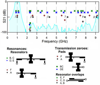
Looking forward to the final design, the positions of the resonances and zeroes found from simulations are given in Fig. 4, showing the expected significant deviation from Fig. 3. The positions of the zeroes are adjusted to provide additional attenuation. Higher order pad zeroes, and all the stub zeroes, are omitted because, with the pad and stub dimensions already chosen, these zeroes are not under the control of the designer.
Zeroes and resonances of individual parts of the final filters. The combined response is shown in light blue. Squares in the resonator layouts indicate input and output. The vertical scale in dB applies only to the combined response; vertical displacements of the points in the graph match the legend. For resonators D and E, a blue cross at 2.3 GHz represents two peaks which cannot be resolved.

IV. FILTER SIMULATIONS AND DESIGN
Two similar sixth-order filters with 1 GHz center frequency and 42% bandwidth were produced. As before [Reference Huang1], only the second filter includes the resistive attenuation. For a new filter, the design procedure would probably be similar to [Reference Huang1], using design data from [Reference Matthaei, Young and Jones29], but here, the device was produced by substituting new pads and resonators into the previous design. The substrate is 1.27 mm thick Duroid RT6010LM with dielectric constant nominally 10.2 according to one measurement technique [30], but as recommended by the manufacturer's latest data sheet [30], the dielectric constant assumed is ε r = 10.6 perpendicular and 13.33 parallel to the surface. The input and output are 50 Ω lines with width 1.25 mm. The SIR resonators have two sections of widths 0.5 mm (72 Ω) and 2.25 mm (36 Ω), while the length of the wide section is 5 mm and the total length is as shown (Fig. 1). Stub dimensions are given in Fig. 3. The stubs have narrow sections of width 0.5 or 1 mm and length 1 mm at the taps, to minimize the magnetic field perturbation in the main line. As in [Reference Huang1], the gap between C and D is 0.625 mm. To avoid small simulation cell sizes, the separation between resonators A and B is 0.25 mm over half the distance, and 0.375 mm over the other half, instead of a uniform 0.3125 mm.
The transmission zeroes introduced by the pads attenuated resonances near 2.3, 5.8 and 7.8 GHz. When making stop-band adjustments, the pad effective area was kept constant to minimize the effect on pass-band coupling coefficient [Reference Huang1]. For example, x eff and y eff can be varied keeping x eff yeff , Y eff −y eff and X eff constant. This changes the pad inductance, which has much more effect in the stop band than in the pass band. Alternatively, X eff and x eff can be changed, also keeping the pad area constant.
For the pass band, external Qs (quality factors) and coupling factors k BC and k DE were adjusted by varying the pad areas. When y eff ≈ Y eff /2, the stop-band variation is minimized by varying y eff , while keeping Y eff constant, as implied by data in [Reference Lin, Deng, Lin, Wang and Chen2]. From Fig. 1, the condition y eff ≈ Y eff /2 is not well satisfied, but this assumption was acceptable considering that the border to allow for edge effects changes Y eff but not y eff (as seen in Fig. 2), that is, y eff = y but Y eff > Y. This condition also leaves pads BC and DE with a sub-optimal value of y eff (which should have been as small as possible, as previously described).
The filter enclosures are modified by 0.5 mm2 vias as the side walls, extending from the ground plane to the roof, 8 mm above the substrate. The positions are shown by the gray squares in Fig. 1. The minimum distance from a pad or resonator is 2.5 mm, while the maximum spacing between wires is 5.5 mm (a sixth of a wavelength at 8.9 GHz, the end of the stop band), with smaller spacing near the convex corners where the field is maximum. According to simulations, this box resonates at 9.7 GHz, which gives a small error margin. The enclosure is vital to avoid long-distance coupling, for example, between resonators A and F. Signal suppression is by reflection and absorption, not radiation: in addition to the rows of vias, there is a rectangular, outer, metal box provided by the software which completely encloses each filter. A commercial implementation is more likely to be a metal-coated, plastic box with the same shape as the wire skeleton box.
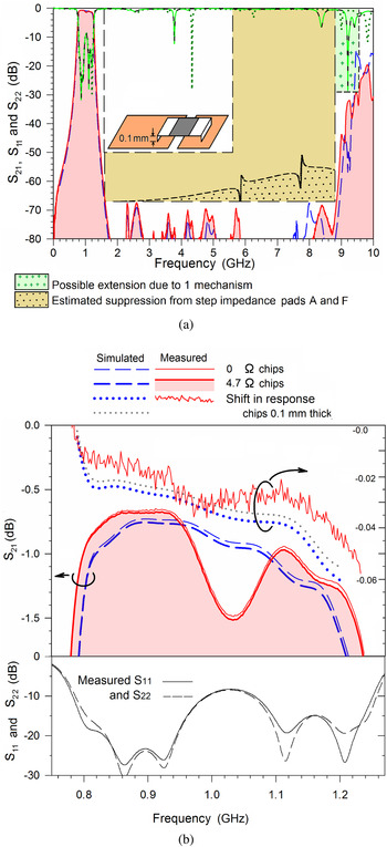
The simulated response of filter 1 is shown as the blue dashed line in Fig. 5 (together with measured results to be discussed in later sections). No spurious responses rise higher than −59 dB, up to 9.0 GHz. For filter 2 (Fig. 6(a)), the simulated suppression level is −69 dB up to 8.9 GHz, assuming flip-chip resistors with the resistive film on the underside of the ceramic chips, and a 0.1 mm air gap between the resistive film and the copper tracks. Simulated pass-band S 21 is shown in Fig. 6(b). The increase in attenuation due to the resistance is shown for both inverted and non-inverted chips, showing that in both cases the additional resistors increase loss by an average of only 0.03 dB, half as much as [Reference Huang1].
Simulated and measured responses of filter 1, without resistors.

(a) Simulated and measured responses of filter 2, with 4.7 Ω resistors. (The legend in Fig. 5 also applies here.) Inset: skeleton representation of a flip-chip resistor. (b). Increase in pass-band loss due to resistors, and pass-band S 11 and S 22.

The improvement contributed by each individual technique was estimated approximately. Comparison with an earlier simulation (not shown) suggests that, by including suppression up to the ninth order, the stagger tuning extends the stop band by ~1.5 GHz. Use of the SIR contributes a similar amount, and the cumulative effect is substantial.
A comparison between rectangular and step-impedance pads in complete filters showed that the latter used only 70% as much substrate area. It also showed a few dB of improvement, but the positions of the zeroes were completely rearranged, so the improvement could well have been due to a different combination of resonances and zeroes; these inconclusive results are not presented.
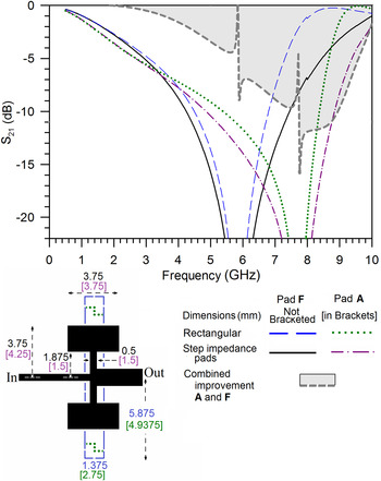
Instead, the notches provided by pads A and F are compared in simulations with rectangular pads in Fig. 7. The rectangular pads were adjusted iteratively to have the same notch frequency and the same pass-band center value of S 21 as their respective step-impedance replacements. The dominant feature of a rectangular or step-impedance pad is the notch, but when they are compared, the subtraction leaves a broad band improvement by the new pads. The two pads combine to give a maximum of about 12 dB at 8.2 GHz, in a region of less widely spaced resonances (Fig. 4), that is, where they are not so well staggered and yet need a relatively broadband suppression method to cover about 12 resonances, equivalent to suppressing two harmonics in a filter with no stagger tuning. The average is 5 dB of the total 20 dB simulated improvement over 1.5–9 GHz, a wider stop band than [Reference Huang1]. Suppression by reduced resonator coupling is discussed approximately in [Reference Huang10].
Comparison between rectangular and step-impedance shapes for pads A and F. Dotted green line in the layout shows the modified rectangle to achieve a mean rectangle height of 4.9375 mm without using small cell sizes.

For the spurious resonances at 2.3 and 2.6 GHz, a graph similar to Fig. 7 (not shown) suggests an improvement of ~1 and 3 dB, respectively, by the combined effect of pads BC and DE. The overall improvement is difficult to estimate because it involves comparing deep higher order notches.
To summarize, the improved stagger tuning therefore contributes most of the improvement in suppression, with a significant contribution from the pads A and F (Fig. 6(a)). The transmission zeroes of pads BC and DE, together with the overlap transmission zeroes, can be concentrated on the lowest frequency spurious response, which was dominant in a previous filter [Reference Huang1].
V. FILTER MEASUREMENTS
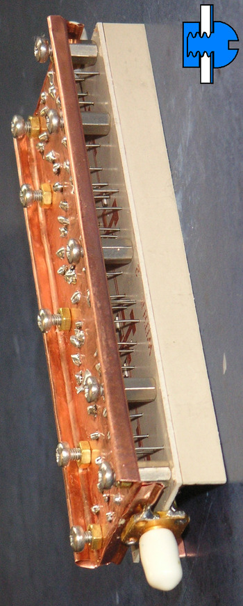
The two filters were fabricated using standard PCB etching by a commercial supplier. A photograph of the complete filter is given in Fig. 8. The vias are 0.56 mm diameter wires (24 SWG, British “Standard Wire Gauge”) and the roof is 150 µ copper sheet. The inset shows a screw and a spacer forming a resonator in the small groove between screw and spacer, simulated and measured results showing resonance at ~7.5 GHz; even a 1 mm deep groove has this resonance because (a) it is a radial resonator, (b) the dielectric fills the gap, and (c) the field can bulge outside the gap. This explains why the spacers in [Reference Huang1] were replaced by wires. The remaining spacers do not form part of the enclosure. The assumption that the suppression is not due to radiation was confirmed by wrapping the filter in aluminum foil: there was negligible change in performance. (Contact between the foil and the rest of the enclosure was unreliable, but tolerable for this single measurement.)
The fully assembled filter 2 (filter 1 is similar). Inset (blue) shows a resonator formed in the groove between a screw and a spacer.

The resistive films were originally on the top of each 3.2 mm × 1.6 mm chip, about 0.5 mm above the filter substrate, making additional space for the magnetic field and shifting some of the resonances downwards, which compromised the stagger tuning. Therefore, on a second copy of filter 2, the chips were soldered upside-down as an approximation for flip chips.
The response of filter 1, without resistors, is given in Fig. 5. Compared with [Reference Huang1], the stop-band level has been decreased from −33 to −54 dB, and the upper pass-band limit improved from 6.3 to 8.9 GHz. In filter 2, with 4.7 Ω resistors, the attenuation is increased from −50 to −67 dB, and stop-band limit from 5.6 to 8.8 GHz. A 5% frequency error present in [Reference Huang1, Reference Huang10, Reference Huang21, Reference Huang22] has been resolved by using the new values of relative permittivity.
The average deterioration in pass-band loss due to the resistors was confirmed to be 0.03 dB by comparing pass-band magnitude before and after changing from 0 Ω bridges to the 4.7 Ω resistors (Fig. 6(b)), in the earlier run where the chips were not inverted. This measurement was not repeated for flip chips because of likely damage from repeated soldering. A typical network analyzer drift over the time taken to re-solder the resistors is 0.007 dB. The box walls were not yet assembled, to allow rapid re-soldering of the resistors. S 11 and S 22 are included in Fig. 6(b); they are not identical because the filter is lossy and not perfectly symmetrical.
VI. COMPARISONS WITH RECENT WORK
The filters were made similar to [Reference Huang1], so that valid comparisons can be made. A crude figure of merit can be obtained considering two reference filters each with stop-band width B s and attenuation α s dB, separated by an isolator (which allows the signal to pass in one direction only). If the two stop bands are adjacent, the combined stop-band width is 2B s , and a new filter with width 2B s should have twice the figure of merit of a reference filter. If the two reference filters have coincident pass bands, then the attenuation is 2α s dB, and a new filter with this level of attenuation should also have twice the figure of merit. The 2α s dB applies only if the worst-case peaks of the two reference filters are coincident. If the isolator is also omitted, the reference filters are not terminated with 50 Ω (or other system impedance) in the stop band and the attenuation may be much less. Subject to these limitations, a figure of merit is α s Bs /f 0, where the pass-band center frequency could optionally be included to allow comparison of frequency-scaled filters.
One of the main original improvements of this work compared with [Reference Huang1] is the introduction of the step-impedance pads to the combination of suppression methods; on their own they contribute an estimated 37 GHz-dB (arbitrary units) of additional attenuation (Fig. 6(a)). This compares favorably against a typical improvement by suppressing one harmonic using one suppression method, which offers a similar suppression to the 0.8 GHz by 29 dB rectangle near 9 GHz in Fig. 6(a), an area of 23 GHz-dB; the step-impedance pads increase attenuation by one-and-a-half times more than this.
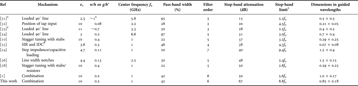
This figure is dwarfed by the overall improvement in the two filters, which have a figure of merit 2.4 times the corresponding filters in [Reference Huang1]. Except for the more complex shape, there are no changes in technological requirements, for example, minimum line widths. Other previous harmonic suppression techniques available in the literature are compared in Table 1. Some of the data are very approximate, having been read off graphs and photographs, or estimated from other data. In some cases, the stop-band limit is the highest frequency given in a graph, which may not do justice to the filter. The present filter 2 has by far the highest stop-band attenuation, and nearly the highest stop-band limit. The relatively large size and long, thin shape are a price for the higher performance.
Some wide pass-band filters with harmonic suppression (partly taken from [Reference Huang1]).

* Smallest width-to-substrate-thickness or gap-to-thickness ratio.
† The center of the pass band is f 0.
‡ DC band not suppressed.
§ Estimated from a small photograph.
¶ Stepped impedance resonator and interdigital capacitor.
Finally, in filter 1, the ratio of stop-band depth to pass-band loss (in dB) is ~54. Cascading a second such filter, using an isolator as above, the stop-band and pass-band losses increase in the same ratio. However, when adding the resistors, the ratio of the increases is ~400:1; the resistors increase stop-band depth without unduly increasing pass-band loss or substrate area, subject to diminishing returns as noted in [Reference Huang1].
VII. CONCLUSION
Spurious responses for wide band microstrip filters were effectively suppressed with a new combination of techniques, giving a greater stop-band width and attenuation. The advantage of a step-impedance pad was also discussed. The filters are larger than chip filters, but compared with other distributed filters, the resonators are significantly smaller than a quarter wavelength, instead of the typical half-wavelength. The pads have narrow waists which allow space for the resonators, shortening the filter compared with [Reference Huang1]. There is scope for reducing the width of the filter further by finding more compact pads.
 Frederick Huang received the B.A. and D. Phil degrees in Engineering Science from the University of Oxford in 1980 and 1984. From 1989 to 2015, he was a lecturer with the University of Birmingham, where after retirement he became an honorary research fellow.
Previous research interests are surface acoustic wave (SAW) dot array pulse compressors, analogue voice scramblers, Langmuir-Blodgett films, SAW and superconducting linear phase and chirp filter synthesis using inverse scattering, slow-wave structures, superconducting quasi-lumped element filters, switched filters and delay lines, together with microstrip and waveguide discontinuities. The main current interests are spiral band-pass filters and filter harmonic suppression.
Dr. Huang is a member of the IET (UK).