I. INTRODUCTION
Since the first demonstration of the La0.7Ca0.3MnO3:MgO nanocomposite system,Reference Lebedev, Verbeeck, Van Tendeloo, Shapoval, Belenchuk, Moshnyaga, Damashcke and Samwer1 the two-phase nanocomposite thin films, holding the promise for multifunctionality, have drawn extensive research interests.Reference Ma, Hu, Li and Nan2–Reference Harrington, Durrell, Wang, Wimbush, Tsai and MacManus-Driscoll4 For example, the BiFeO3 (BFO):CoFe2O4 (CFO) nanocomposites combine ferroelectric and magnetic properties together achieving multiferroic characteristics.Reference Zheng, Wang, Lofland, Ma, Mohaddes-Ardabili, Zhao, Salamanca-Riba, Shinde, Ogale, Bai, Viehland, Jia, Schlom, Wuttig, Roytburd and Ramesh5 Following that, a unique family of two-phase nanocomposite with vertical lattice alignment, termed as the vertically aligned nanocomposites (VAN), has been demonstrated in several systems.Reference MacManus-Driscoll, Zerrer, Wang, Yang, Yoon, Fouchet, Yu, Blamire and Jia6, Reference Yang, Wang, Yoon, Wang, Jain, Feldmann, Dowden, MacManus-Driscoll and Jia7 For example, the La0.5Sr0.5CoO3 (LSCO):Ce0.9Gd0.1O1.95 (CGO) VAN was fabricated as the interfacial layer between the cathode and the electrolyte and proven to effectively increase the cell efficiency in solid oxide fuel cells.Reference Yoon, Cho, Kim, Lee, Bi, Serquis, Zhang, Manthiram and Wang8 More interestingly, the strain coupling along the vertical lattice matched interfaces in VAN systems can be further tuned by the diameter and density of the nanopillars.Reference Bi, Lee, Yang, Jia, MacManus-Driscoll and Wang9, Reference Chen, Bi, Tsai, Lee, Su, Zhang, Jia, MacManus-Driscoll and Wang10 New functionality and unique strain coupling are attractive for future applications; however, fundamental study on the vertical lattice matching and the nature of the defects along the vertical interfaces is scarce in the literature.
On the other hand, in the field of high-temperature superconductors (HTS) such as YBa2Cu3O7-(YBCO),Reference Wu, Ashburn, Torng, Hor, Meng, Gao, Huang, Wang and Chu11 maintaining the critical current density Jc of the film under applied magnetic field, i.e., excellent in-field performance, is one of the major challenges for practical applications.Reference Foltyn, Civale, MacManus-Driscoll, Jia, Maiorov, Wang and Maley12 One of the main approaches is to introduce nanoscale defects in YBCO matrix, which serve as the flux-pinning centers under high fields.Reference Foltyn, Civale, MacManus-Driscoll, Jia, Maiorov, Wang and Maley12, Reference Wimbush, Durrell, Tsai, Wang, Jia, Blamire and MacManus-Driscoll13 These dopants have to be chemically compatible with YBCO and be capable of growing epitaxially in the YBCO matrix. Among all of the artificial pinning centers introduced including the 0D,Reference Haugan, Barnes, Wheeler, Meisenkothen and Sumption14 1D,Reference Dam, Huijbregtse and Rector15, Reference MacManus-Driscoll, Foltyn, Jia, Wang, Serquis, Civale, Maiorov, Hawley, Maley and Peterson16 and 2DReference Foltyn, Wang, Civale, Jia, Arendt, Maiorov, Li, Maley and MacManus-Driscoll17 defects; to date, vertically aligned nanopillars are considered to be one of the most effective pinning schemes. For example, Goyal et al. showed a stronger pinning effect along c-axis for BaZrO3 nanorods doped YBCO films.Reference Kang, Goyal, Li, Gapud, Martin, Heatherly, Thompson, Christen, List, Paranthaman and Lee18 Varanasi et al. demonstrated the BaSnO3 (BSO)-doped YBCO films with significantly enhanced c-axis pinning effects.Reference Varanasi, Burke, Brunke, Wang, Sumption and Barnes19, Reference Varanasi, Burke, Brunke, Wang, Lee and Barnes20 Recently, Wee et al. chose Ba2GdTaO6Reference Wee, Goyal, Specht, Cantoni, Zuev, Selvamanickam and Cook21 and Ba2YNbO6Reference Wee, Goyal, Zuev, Cantoni, Selvamanickam and Specht22 which chemically and structurally similar to YBCO as the secondary phase, achieving self-assembled growth as well as flux pinning enhancement. However, the nature of the defects and the effects of the strainReference Cantoni, Gao, Wee, Specht, Gazquez, Meng, Pennycook and Goyal23 along the vertical interfaces that could be responsible for superconductive performance are still under investigation.
In this work, we select BSO-doped YBCO films with different doping concentrations as the typical system to investigate the microstructural origin of the VAN growth and the nature of the defects along the heterogeneous interface in the systems. The reasons BSO-doped YBCO system is chosen for this study are (i) BSO nanopillars grow epitaxially in YBCO matrix over a large thickness range; and (ii) the BSO nanopillar density can be easily tuned over a wide range by controlling the doping concentration of BSO. A combination of cross-section and plan-view transmission electron microscopy (TEM) study was applied to all the VAN films with different doping concentrations for exploring the distribution and dimension of the BSO phases. The out-of-plane lattice strain and matching relation of YBCO and BSO were studied for exploring the possible growth mechanisms of the self-assembled BSO nanopillars.
II. EXPERIMENTAL
Depositions of YBCO thin films with different BaSnO3 concentrations (2 mol%, 4 mol%, 10 mol%, and 20 mol%) were conducted using pulsed laser deposition (PLD). The ratio of YBCO to BSO in the resulting thin films was controlled by varying the amount of powders in the composite targets preparation. Starting with commercially available YBCO (Nexans, Hurth, Germany) and BSO powders (Cerac, Milwaukee, WI), which were carefully weighed and well mixed to achieve four final targets with 2 mol%, 4 mol%, 10 mol%, and 20 mol% BSO in YBCO, respectively. Then, four composite films, up to a thickness of approximately 300 nm, were obtained on (100) LaAlO3 (LAO) single crystal substrates. The details on target processing and deposition details can be found elsewhere.Reference Wee, Goyal, Specht, Cantoni, Zuev, Selvamanickam and Cook21
A systematic microstructural characterization was conducted via x-ray diffractometer (XRD) and TEM. Plan-view and cross-section TEM samples were prepared through a conventional TEM sample preparation routine including cutting, gluing, grinding, polishing, and final precision ion polishing. The TEM characterization was performed using a Philips CM200F analytical electron microscope with a point-to-point resolution of 0.20 nm.
III. RESULTS AND DISCUSSION
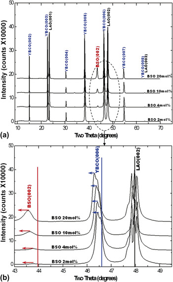
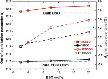
The overall microstructure of the YBCO/BSO films was first characterized by XRD. In Fig. 1(a), all the films show primarily YBCO (00l) peaks and BSO (002) peaks in the typical θ–2θ scans, indicating that all four composite films are highly textured along YBCO (00l) on LAO (001) substrates. As the BSO concentration increased from 2 mol% to 20 mol%, the corresponding BSO (002) peak intensity also increased while no other peaks from other BSO orientations or other impurity phases were observed. This suggests that the primary (002) orientation remains as BSO doping concentration increases. Under this orientation relationship of YBCO(00l)//BSO(00l)//LAO(001), the theoretical lattice misfit rate, as well as corresponding coherent matching dislocation spacing and residual strains are calculated using the bulk lattice constants for the lateral and the vertical interface, respectively. As listed in Table I, in the epitaxial thin film, besides the conventional lateral lattice confinement from the substrate, a lattice misfit of ∼5.535% between the two film phases–YBCO and BSO-is suggested. It is interesting to note that, as shown in the enlarged XRD pattern in Fig. 1(b) with all diffraction peaks normalized based on the strongest LAO (002) peak, both YBCO (006) and BSO (002) peaks shift toward lower angles, i.e., larger out-of-plane lattice parameters, as the BSO concentration increases. The ratio of YBCO (006)/(005) peak intensity was calculated for each sample and remained relatively constant. It indicates little or no variation in oxygen stoichiometry of the YBCO matrix for all the samples, which is in agreement with the fact that all of the films were prepared under the same PLD conditions. The calculated dc of the YBCO matrix and of the BSO secondary phase, as well as their increases as a function of doping concentration is then presented in Fig. 2. Comparing to the dc of a 280-nm-thick pure YBCO thin film (∼11.704 Å), the out-of-plane dc of the YBCO phase in the doped thin films only shows a very small variation. However, the dc of the BSO secondary phase increases about 0.6% when the doping concentration rises to 20 mol%.
XRD θ–2θ scans of YBCO samples with 2 mol%, 4 mol%, 10 mol%, and 20 mol% BSO in: (a) the full range; (b) the enlarged XRD scan showing YBCO (006) and BSO (002) peaks. All diffraction patterns are normalized with the strongest LAO (002) peak. The peak positions of bulk YBCO and BSO are noted in (b) as solid line for reference. (color online)

The plot of XRD out-of-plane lattice parameter and corresponding percentage variations of the YBCO and the BSO in all four samples. (color online)

The list of theoretical in-plane and out-of-plane lattice misfit, dislocation spacing calculated by bulk lattice parameters at room temperature.

Note: for the vertical strain prediction, the dc(001) of YBCO is divided by three, i.e., the averaged c/3 = 3.894Å, for simplification. In the calculation of dislocation spacing, d002 s is adopted considering the actual (002) monolayer matching.
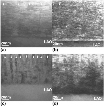
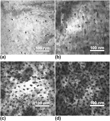
To explore how the BSO secondary phase disperses in the YBCO matrix and the related defects caused by the dopant structures, we conducted both plan-view and cross-section TEM (XTEM) studies on all the composite films. Figure 3 shows low magnification XTEM images of YBCO + BSO films on LAO substrates with BSO doping concentration varied from 2 mol% to 20 mol%. It is noted that nicely grown BSO nanopillars align vertically throughout the film thickness. With the increase of BSO concentration, these vertically aligned nanopillars were not growing wider; instead, their density increases accordingly. A clear illustration of the dimension and distribution of the BSO nanocolumns with different doping concentrations is presented in the plan-view TEM images in Fig. 4. As the BSO concentration increases from Fig. 4(a) 2 mol% to Fig. 4(d) 20 mol%, the nanopillars density increases from 2.60 × 10¹⁰/cm2 to 1.44 × 10¹¹/cm2 while the diameter of the nanocolumns remained relatively constant at about 7–8 nm in diameter.
Low magnification XTEM images of YBCO/BSO composites on LAO substrates with (a) 2 mol%, (b) 4 mol%, (c) 10 mol%, and (d) 20 mol% BSO, respectively. High-density vertically aligned BSO nanocolumns are cleared observed in all four samples and marked as white triangles.

Plan-view TEM micrographs of YBCO/BSO composites with (a) 2 mol%, (b) 4 mol%, (c) 10 mol%, and (d) 20 mol% BSO, respectively. The as-observed elliptic cross-sections of the BSO nanocolumns are due to an angle between the sample surface normal and the column axis. The diameter of the BSO nanocolumns was estimated from the shorter radius.

From the above XRD and TEM analysis, it is obvious that the YBCO + BSO films have grown as heteroepitaxial two-phase VAN. Different from most of the other artificial secondary phases, e.g., nanoparticles like BaZrO3 (BZO)Reference MacManus-Driscoll, Foltyn, Jia, Wang, Serquis, Civale, Maiorov, Hawley, Maley and Peterson16 and Y2O3Reference Wang and Wang24 or nanolayers such as CeO2Reference Foltyn, Wang, Civale, Jia, Arendt, Maiorov, Li, Maley and MacManus-Driscoll17, Reference Barnes, Haugan, Varanasi and Campbell25 and Y2BaCuO6Reference Haugan, Barnes, Wheeler, Meisenkothen and Sumption14, the BSO continuous nanopillars in the VAN structure grew epitaxially and simultaneously with YBCO matrix through the film thickness. Based on the Winterbottom constructionReference Winterbottom26 and recently presented guidelines to the materials selection of the self-assembled vertical nanocomposites,Reference MacManus-Driscoll, Zerrer, Wang, Yang, Yoon, Fouchet, Yu, Blamire and Jia6 the intrinsic similarity in crystalline structures and out-of-plane lattice matching between the cubic Perovskite BSO and YBCO matrix, as well as the comparable wetting ability to the surface of (001) pseudocubic LAO substrate for both phases, these developments indicate the tantalizing possibility of heteroepitaxy BSO in 3D (i.e., both in-plane as well as out-of-plane). Compared with another frequently used secondary addition—BZO—which forms continuous nanorods only under certain PLD conditions and many of the BZO nanorods were observed bent as film thickness increases;Reference Mele, Matsumoto, Horide, Ichinose, Mukaida, Yoshida, Horii and Kita27 BSO nanopillars intend to maintain the steady straight growth, despite our efforts in trying to break their continuity by raising deposition temperature during the PLD process. Thus, the proposed 3D heteroepitaxy was found to be quite robust in the PLD-grown BSO/YBCO system and also in other REBa2Cu3Oy (RE: rare-earth element) films.Reference Ichinose, Mele, Horide, Matsumoto, Goto, Mukaida, Kita, Yoshida and Horii28 The detailed self-assembled growth dynamics and morphology control of the nanostructures have been studied as one of the fundamental issues of the self-assembled nanocomposites,Reference Winterbottom26 which are beyond the scope of this work. Here, we are trying to further investigate the lattice matching between the two phases that one occupies dominant film volume than the other; and to explore how they accommodate the challenge of an extra heterogeneous interface achieving the VAN structure.
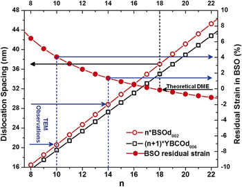
The strain state of the 300 nm-thick YBCO + BSO VAN film is determined by two competing factors, i.e., the lateral strain from the substrate and the vertical strain between the two phases. To determine which one is dominant, the ratios of the vertical to lateral interface areas for BSO and YBCO are listed in Table II, in 2 mol% and 20 mol% samples respectively. For BSO, apparently the vertical interface area between BSO and YBCO is much larger (about 150 times larger) than the lateral interface, due to the very small BSO nanopillar diameter. This suggests that the vertical strain is dominant in the BSO nanocolumns, and it seems unaffected by the doping concentration. According to the theoretical predications listed in Table I, since BSO has a larger c-lattice parameter of 4.116 Å than the c/3 of YBCO (3.894 Å), a large vertical compression (∼5. 385%) is expected in BSO in the ideal coherent lattice matching. However, as shown in Fig. 5, the vertical BSO/YBCO interface observed in practice suggests otherwise. HRTEM images of the 4 mol% and 20 mol% samples, and their corresponding fast Fourier filtered images are shown in Figs. 5(a)–5(d), respectively. Along the interface between BSO and YBCO, localized dislocation-like contrast [marked as white “T” in Figs. 5(b) and 5(d)] was observed in both samples. Taking the 4 mol% sample for instance, the misfit dislocation spacing (dM) measured here in Fig. 5(b) is only ∼3 nm, indicating a domain matching epitaxy (DME)Reference Narayan and Larson29 where 14 of (002) BSO lattices match with 15 of (006)YBCO lattices. Under such matching condition, the residual strain in BSO yields a vertical tension ∼1.3%. The same filtered Fast Fourier Transformation (FFT) was applied to the high-resolution TEM (HRTEM) images taken at the vertical interfaces from samples with different doping concentrations. Although it is not conclusive that the VAN film with higher BSO concentration has a smaller dM, a dM of ∼2 nm, resulting in an even larger residual strain ∼4% in BSO, is observed at a section of vertical interface in the 20 mol% sample. Based on the theoretically predicted dislocation spacing (Table I), the ideal dislocation spacing is ∼3.7 nm, yielding a very small residual compression ∼−0.05% in the BSO (as shown by the black arrows in Fig. 6). However, practically, the dislocation spacing along the vertical interface is smaller (2–3 nm) than the theoretically calculated value, as illustrated by blue arrows in Fig. 6. This modified DME, thus, introduces considerably large residual tension in the BSO.
TEM observations at the BSO-YBCO vertical interface and the schematic illustration of the flux-pinning effect of the vertical interfacial defects under applied magnetic fields. HR-XTEM images and corresponding filtered FFT images are shown in (a) and (b), (c), and (d) for the 4 mol% and 20 mol% film, respectively. Misfit dislocations are marked as white “T” along the vertical interface. In (e), the thickness of the YBCO thin film is noted as h; the radius of the nanopillar is noted as r, respectively. When transport current (I) is applied under the magnetic field (B), the resulting Lorentz force (FL) moves vortices toward right (showing by curved vortices line in red), dissipating energy and causing the electric resistivity to occur. The vertical-interfacial-defects and their effects in pinning the vortices lines are illustrated in terms of the defects density. The misfit dislocation lines are noted as dotted lines around each doping phase. (color online)

The plots of the dislocation spacing and BSO residual strain variation as a function of the domain epitaxy matching n. Black arrows and dashed lines guide the view of theoretical domain matching epitaxy; blue lines guide the TEM observed matching results in the YBCO/BSO nanocomposite film. The practical dislocation spacing (or domain size), as shown, is smaller than the theoretical prediction, resulting in the reverse in the vertical strain state of BSO. (color online)

Calculations of the vertical to lateral interface areas ratios of the BSO and the YBCO in the VAN films with 2 mol% and 20 mol% BSO, respectively.

Note: r refers to the radius of the BSO nanocolumn which is about 4 nm measured by TEM; h = 300 nm is the film thickness.
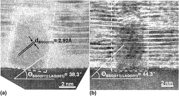
Moreover, besides the above lattice extension/compression, local lattice rotation related to the tilting growth of the BSO nanopillars, is also observed in the VAN films, especially those with low BSO concentration. As shown in Fig. 7(a), a BSO nanopillar in a 4 mol% film has a ∼6° tilt off the c-axis. It is surrounded by an amorphous-like area with a thickness of 2–3 unit cells (∼2.5 nm). While in the samples with higher BSO doping concentrations, such as Fig. 7(b), a thinner amorphous region (∼1 nm) is found mainly on the left side of a straighter BSO nanopillar in the 20 mol% sample. From our experience, the emerging of amorphous-like layers between YBCO and substrate could be introduced by TEM foil preparation. Whereas, these observed tilting growth is more likely attributed to the large lattice mismatch between BSO and LAO substrate (∼−8.273%). Since YBCO competes with BSO during the initial film growth, it could be difficult for BSO to grow laterally and become wide enough to form domain matching epitaxy. One effective way of relieving this large lateral strain is tilting the BSO nanopillars slightly off the c-axis. And this titling growth could, in turn, impact the local out-of-plane and in-plane contact lattice relationship.
The enlarged XTEM images of the film/substrate regions of the YBCO + BSO film with (a) 4 mol% and (b) 20 mol% BSO, respectively. The BSO nanopillars’ tilting angles are characterized by the angle between the BSO(011) and LAO(001), which is 45° in idea case.

In all, a great number of dislocations with spacing 2–3 nm were observed along each BSO-YBCO vertical interface, and the dislocation density increases as the number of BSO nanopillar increases. Conventionally, interfacial defects, especially misfit dislocations, are of great interest in functional oxide thin films.Reference Blamire, MacManus-Driscoll, Mathur and Barber30 For example the film-substrate interfacial defects are believed to be responsible for the high Jc of YBCO and attribute to the thickness dependence effect of YBCO films.Reference Foltyn, Wang, Civale, Maiorov and Jia31 For this BSO-YBCO VAN case, the BSO nanopillars as well as the defects along the interfaces between the BSO and YBCO are the effective pinning centers for the enhanced in-field performance.Reference Varanasi, Burke, Brunke, Wang, Sumption and Barnes19, Reference Varanasi, Burke, Brunke, Wang, Lee and Barnes20 A recent study on BaZrO3 doped YBCO films (BZO/YBCO) shows that the strain induced oxygen stoichiometry variation along the interfaces could also affect YBCO’s superconducting performance.Reference Cantoni, Gao, Wee, Specht, Gazquez, Meng, Pennycook and Goyal23 In the BSO/YBCO case, the Tc of YBCO maintains a high value of >87 K for all concentrations.Reference Varanasi, Burke, Brunke, Wang, Lee and Barnes20 Therefore the effects of oxygen stoichiometry variation in the BSO/YBCO case might not be as strong as that in the BZO/YBCO case. A schematic illustration of the defect distribution and corresponding pinning effects of the VAN YBCO thin films is presented in Fig. 5(e). Under the applied magnetic field (B), the resulting Lorentz force (FL) could move vortices toward right (illustrated by the red vortices’ line), dissipating energy and causing the electric resistivity to occur. As illustrated here, the vertically aligned BSO nanopillars can provide the possibility of arranging the pinning centers throughout the YBCO film thickness and achieving a much stronger pinning effect especially for high-field applications. The above defects analysis and discussions agrees well with the Jc results measured in applied magnetic field,Reference Varanasi, Burke, Brunke, Wang, Lee and Barnes20 which showed an obvious enhancement in Jcin-field (H//c) as the YBCO doped with higher BSO concentrations. Therefore, although the accurate control on the density of the vertical interfacial defect is complex, VAN configuration is a promising approach for introducing and, more importantly, distributing the flux-pinning defects throughout the film thickness and forms a 3D defect network.
IV. SUMMARY
In conclusion, we have conducted in-depth microstructural characterizations on the PLD-grown BSO/YBCO VAN to explore the growth mechanism and vertical strain tuning of VAN. In all four YBCO films with the BSO doping concentration varied from 2 mol% to 20 mol%, continuous BSO nanopillars with nearly constant diameters of around 7–8 nm, grow epitaxially and distribute randomly in the YBCO matrix. XRD results suggest a strong lattice strain tuning between the YBCO matrix and the doped BSO nanopillars as a function of the nanopillar density. It was noted that along their vertical heterogeneous interfaces, a high density of dislocations in the order of 1013/cm2 is found throughout the YBCO film thickness. These high-density vertical interfacial defects could act as strong c-axis pinning centers and be responsible for the high-field performance of YBCO films regardless of the film thickness.
ACKNOWLEDGMENTS
This research was funded by the Air Force Office of Scientific Research (Contract No.: FA9550-09-1-0114), and AFRL–Propulsion Directorate. The TEM characterization effort was supported by National Science Foundation (NSF-0846504). J.H. Kwon was supported by the Undergraduate Summer Research program at Texas A&M University.